• Hey, guest user. Hope you're enjoying NeoGAF! Have you considered registering for an account? Come join us and add your take to the daily discourse.

WiiU "Latte" GPU Die Photo - GPU Feature Set And Power Analysis

Status
Not open for further replies.
This is kinda off-topic but I can't really make a thread as a junior member.

Here is Nintendo's view of their hardware:
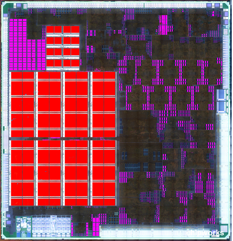
I don’t want to talk about anything too technical, but in my view, Wii U is a console with low power consumption and has fairly high performance. Regarding your comment that we focus on the GPU and that the CPU is a little poor, we have a different view. It depends on how to evaluate a processing unit. In terms of die size (area a chip occupies), the GPU certainly occupies a much larger space than the CPU. As you can see CPUs used for the latest PCs and servers, however, it is usual for current CPUs that the logic part for actual calculations is really small and that the cache memory called SRAM around it covers a large area. From this angle, we don’t think that the performance of the Wii U’s CPU is worse than that of the GPU. In other words, we have taken a so-called "memory-intensified" design approach for the Wii U hardware. It is no use saying much about hardware which should remain in the background in our entertainment offerings, but at least we think that Wii U performs pretty well.

In regard to GPUs, they are so advanced that other companies in the video game market seem to be on the same path. Developers have also been accustomed to programmable shaders to create games. In this sense, we think that the entire industry, including Nintendo, has had less trouble in this field than in the time when shaders were emerging.

http://www.nintendo.co.jp/ir/en/library/events/130131qa/02.html
 

Schnozberry

Member
Well, what I'm saying is that it might be something a lot simpler than "secret sauce" (at least for the most part). Asymmetric registers would definitely be unusual, but it's not like creating some crazy fixed function hardware from scratch, and would in fact be pretty simple to implement and only a relatively minor hassle to code for.

Interesting idea. Do you have any areas on the chip itself that look arranged in a way that would add some evidence of this?
 

Elios83

Member
You know the reason for the coffee based naming convention?

The WiiU's internal development name was 'Project Cafe' The CPU is know as 'Espresso'.

Ah no I didn't know that, so it has a sense and it's pretty funny.
So coffe (espresso) + milk = cappuccino :D

Yes, but the GPU for that one outputted 0 GFlops.

EE did everything.

Yeah you're right, the GS is just a rasterizer, still I thought the Wii U CPU was similar to one of the cores in the 360 CPU....if it's 12 Gigaflops it's much weaker...although of course there's a different design philosophy behind the whole system (GPGPU).
 

japtor

Member
Gotcha. Back on topic... With thraktor's analysis a few posts ago s it plausible that there could actually be some sort of "secret sauce" as he says? I'm nowhere near the technical expert but looking at the die photo what he says about the shaders makes sense. Also if there was one thing that devs seemed to agree on was their satisfaction with the gpu.
Not sure it'd be considered "secret sauce" (which seems to imply awesomeness) as much as just a complete unknown it seems, going by the complete lack of info on what the rest of the die space logic does. Could be good or bad but right now it's just another question mark.

...in a sense we're kind of back to where we were last year in terms of random speculation. It's more grounded with more info to help out now to get a ballpark idea of performance, but still seemingly clueless about large chunks of the equation.
 

Thraktor

Member
Did AMD make this thing a super custom part?

Yes. It's very distinctively different from anything they've ever made using VLIW architecture (that's their entire HD2000-HD6000 lines of GPUs).

Interesting idea. Do you have any areas on the chip itself that look arranged in a way that would add some evidence of this?

Not directly, but consider that Durante identified 6 different classes of obviously repeating components in the GPU logic. A GPU would typically only be expected to have three (shader bundles, TMUs and ROP bundles). Consider also the minuscule portion of the GPU logic that would be allocated to shaders, TMUs and ROPs if we were to assume they were all symmetric. I can't think of a plausible explanation for dedicating ~70% of the GPU logic to custom hardware units. I'm open to hearing people's theories, but I can't think of one myself.

That leaves one possibility: that the normal GPU components take up a larger proportion of the die, and are hence asymmetric in some way. This fits what Nintendo have done with the CPU, and more closely matches expected performance levels. It's also a relatively simple and plausible customisation of the GPU in the scheme of things.
 

Elios83

Member
That would have made people complain even more than they did about the Wii name.


An espresso coffee with milk is called a Latte, not really a cappuccino

LOL I love how italian words are completly misused :p
Latte is milk in italian, so I don't get how adding coffe to milk you get...milk again :D
And what do you mean by cappuccino?
 
Yeah you're right, the GS is just a rasterizer, still I thought the Wii U CPU was similar to one of the cores in the 360 CPU....if it's 12 Gigaflops it's much weaker...although of course there's a different design philosophy behind the whole system (GPGPU).
In general purpose it's actually better; which is a plus.

Floating point precision is lacking, yes.
 

prag16

Banned
If we are actually looking at asymmetric shaders here, then it's possible that it's a 480 SPU chip, or 528Gflops.

In a 15W envelope at 40nm??

Or are we thinking the GPU has somewhat more than 15W to work with (I know that's only a guess)?
 

Schnozberry

Member
Not directly, but consider that Durante identified 6 different classes of obviously repeating components in the GPU logic. A GPU would typically only be expected to have three (shader bundles, TMUs and ROP bundles). Consider also the minuscule portion of the GPU logic that would be allocated to shaders, TMUs and ROPs if we were to assume they were all symmetric. I can't think of a plausible explanation for dedicating ~70% of the GPU logic to custom hardware units. I'm open to hearing people's theories, but I can't think of one myself.

That leaves one possibility: that the normal GPU components take up a larger proportion of the die, and are hence asymmetric in some way. This fits what Nintendo have done with the CPU, and more closely matches expected performance levels. It's also a relatively simple and plausible customisation of the GPU in the scheme of things.

Interesting. It's too bad this will likely not be easy to corroborate with anyone working on the hardware due to NDA's, so we're left to educated guesswork. Do you expect any other customizations on the CPU aside from cache, perhaps something to help with the perceived floating point deficiencies?
 

guek

Banned
If we are actually looking at asymmetric shaders here, then it's possible that it's a 480 SPU chip, or 528Gflops.

That'd be swell. It'd also probably make USC-fan pop a stitch, though I do share his skepticism of that much performance pulled from such low wattage (but without his trademark crassness).
 

Datschge

Member
Thanks to Chipswork and everyone involved for making this possible. No thanks for all the noise though.

With this design, can the fixed function units and the shader units be used to process separate tasks?

The SIMD units can be used to process physics while the fixed function units be used to process graphics?

That's seems like a pretty good design advantage to me.

Looking at the rather meagre space used for the 8 SPs and all the unaccounted space around it I'm pretty confident to say that fixed function units still play a huge role on this GPU, and the fact that it and shaders coexists should allow fo the GPGPU stuff that Iwata already publicly talked about.

my attempt at coloring:
c10234f5_poly_b20hacz.png

red = eDRAM
pink = L1/L2 cache
black = logic
light blue = Audio DSP
white = IO
blue = power connectors?
Green = ARM core/ PCB

Appears to be pretty spot on. Most helpful picture for those who may not know yet how to interpret the typical patterns on the chip. Warrants a mention in the OP imo.

Alright, I've been doing a few calculations around the die size. The total die is 146.48mm², and of that about 50.78%, or 74.38mm² is what I'll call "GPU logic" (that is, everything except the memory pools and interfaces). Now, looking at Durante's image from the first page:

Let's assume, for a minute, that the four blue sections are TMUs, the red sections are shader clusters, and the two yellow sections down at the bottom right are ROP bundles. This would, we assume, produce a core configuration of 320:16:8. Now, if you measure out the sizes of these, you get only 28.9% of the total GPU logic space, just 21.48mm². What's going on with the other 52.9mm² of GPU logic? There's probably a DSP and ARM on there, but that accounts for a couple of mm² at most.

There are basically two possibilities here:

- The 320:16:8 core config is accurate, and there's ~50mm² of custom logic or "secret sauce" (more than twice the size of the conventional GPU logic).

I expect the custom logic to be built up (possibly modernized) from Broadway/Hollywood. Considering the (in relation) huge area it occupies it should be really powerful, and if Nintendo/AMD played the cards right the fixed function units now account for the more common modern usecases for shaders, essentially working as more efficient speed lanes for what could be done in the SPs as well.
 

Thraktor

Member
In a 15W envelope at 40nm??

Or are we thinking the GPU has somewhat more than 15W to work with (I know that's only a guess)?

Most estimates I've heard have given the GPU 25-30W to work with. Besides, we know the GPU is clocked at 550Mhz, and we know how big it is. That logic is doing something, and it's doing it at 550MHz. Whether it's being used for computation (glfops) or something else won't have much effect on the energy consumption.
 

USC-fan

Banned
In a 15W envelope at 40nm??

Or are we thinking the GPU has somewhat more than 15W to work with (I know that's only a guess)?

Like every thread on the wiiu. Couple weeks people on here will be back at wiiu is 600glfop because it has special sauce or whatever kind of bs they come up with.

You have 33 watts to power the system. I really dont even know how they are powering 320:16:8 at 550. Then you add all the other stuff its just not adding up. Something got to give. 33 watts is a hard number, that all we have to work with...

That 15 watts was just not for the gpu parts but the whole gpu die..

Most estimates I've heard have given the GPU 25-30W to work with. Besides, we know the GPU is clocked at 550Mhz, and we know how big it is. That logic is doing something, and it's doing it at 550MHz. Whether it's being used for computation (glfops) or something else won't have much effect on the energy consumption.
done the math

33 watts max from wall @ 90% psu ~30 watts

Disk drive ~4 Watts
Cpu ~8 watts

Whats left ~18

My guesses, anyone have hard numbers
2GB DDR3 Ram ~2 Watts
wifi ~.5 Watts
Flash Storage .5 Watts

Leaves about 15 watts for the whole gpu chip
 

NBtoaster

Member
Most estimates I've heard have given the GPU 25-30W to work with. Besides, we know the GPU is clocked at 550Mhz, and we know how big it is. That logic is doing something, and it's doing it at 550MHz. Whether it's being used for computation (glfops) or something else won't have much effect on the energy consumption.

That would mean the CPU, disc drive, and other parts are just working with 3W?
 

Thraktor

Member
That would mean the CPU, disc drive, and other parts are just working with 3W?

3-8W, yes. Given the disc drive is likely CAV (which requires less power), the CPU is small and very low power, and the other components are almost certainly likewise, then it makes sense for the GPU die to be using the vast majority of the system's power budget.
 

AzaK

Member
To be honest, I simply can't find any logical reason for the first. What would you do with that quantity of custom hardware? Have they discovered some sort of magical Mario rendering technique that demands over two thirds of the GPU logic?

If you look at the 4870 die shot, it does have a lot of extra stuff around the edges and some of that looks uniform and/or duplicated pieces. Maybe it's just the glue that's needed?

die-shot.jpg


Like every thread on the wiiu. Couple weeks people on here will be back at wiiu is 600glfop because it has special sauce or whatever kind of bs they come up with.

You have 33 watts to power the system. I really dont even know how they are powering 320:16:8 at 550. Then you add all the other stuff its just not adding up. Something got to give. 33 watts is a hard number, that all we have to work with...

That 15 watts was just not for the gpu parts but the whole gpu die..


done the math

33 watts max from wall @ 90% psu ~30 watts

Disk drive ~4 Watts
Cpu ~8 watts

Whats left ~18

My guesses, anyone have hard numbers
2GB DDR3 Ram ~2 Watts
wifi ~.5 Watts
Flash Storage .5 Watts

Leaves about 15 watts for the whole gpu chip

Can you explain that bit? The PSU is 75w, so couldn't you expect a draw of 40ish or more?
 

AlStrong

Member
(shader bundles, TMUs and ROP bundles).

In terms of HW blocks & design, one might consider that the colour blocks are in fact separate from the ones handling depth and also blending rather than consolidating them all into a monolithic block.

That leaves one possibility: that the normal GPU components take up a larger proportion of the die, and are hence asymmetric in some way. This fits what Nintendo have done with the CPU, and more closely matches expected performance levels. It's also a relatively simple and plausible customisation of the GPU in the scheme of things.

Don't forget the command processor that tells the GPU what to do along with the geometry/triangle setup that needs to be accounted for. :)

I haven't followed the discussion here so far but there is ( or could be) also: media decode, ARM/Starlet (system IO, security), legacy Hollywood, GamePad vid-stream encode, DSP, display controller.
 

ozfunghi

Member
Most estimates I've heard have given the GPU 25-30W to work with. Besides, we know the GPU is clocked at 550Mhz, and we know how big it is. That logic is doing something, and it's doing it at 550MHz. Whether it's being used for computation (glfops) or something else won't have much effect on the energy consumption.

Is this speculation of you alone, or do any of the other guys (Blu, Durante, Wsippel, AlStrong...) share this opinion?

Because i don't trust you...

i'm kidding
 

AlStrong

Member
If you look at the 4870 die shot, it does have a lot of extra stuff around the edges and some of that looks uniform and/or duplicated pieces. Maybe it's just the glue that's needed?

die-shot.jpg

Going clockwise from bottom left, you're basically looking at the render back ends (they're they last step before outputting to RAM.

The bottom middle I believe is geometry setup/command processor. Bottom right is the UVD/display controllers.
 

Thraktor

Member
If you look at the 4870 die shot, it does have a lot of extra stuff around the edges and some of that looks uniform and/or duplicated pieces. Maybe it's just the glue that's needed?

die-shot.jpg

Most of the area to the top and left is ROPs. At the bottom right there's some video decode hardware, etc. There is certainly some miscellaneous logic on there, but it's a lot closer to 10-20% than it is to 70%.
 

USC-fan

Banned
Can you explain that bit? The PSU is 75w, so couldn't you expect a draw of 40ish or more?

The 33 watts is what the console uses at the wall. We can all measure that and this is the same for running any wiiu games. Been tested by many different sites.
 

EloquentM

aka Mannny
Roller coaster indeed. also, I was not aware that USC-fan was a techie. the first time I saw him post he seemed like any other ordinary nintendo troll.
 

Thraktor

Member
In terms of HW blocks & design, one might consider that the colour blocks are in fact separate from the ones handling depth and also blending rather than consolidating them all into a monolithic block.

Thanks. Would there be any reason that separating them out would make sense to you from a design perspective?

Don't forget the command processor that tells the GPU what to do along with the geometry/triangle setup that needs to be accounted for. :)

I haven't followed the discussion here so far but there is ( or could be) also: media decode, ARM/Starlet (system IO, security), legacy Hollywood, GamePad vid-stream encode, DSP, display controller.

There's certainly some such units, but it simply wouldn't make sense to me that they should take up that proportion of the die. If you were to look at Durante's diagram and say (for instance) that the red and blue blocks are the shaders, the teal and green are the TMUs and the yellow and pink are the ROPs, you still have ample space for all the sundries and custom bits'n'bobs (probably about 40% of the logic), but with a much more reasonable proportion of the die dedicated to the actual GPU parts.

Edit: Here's my original post on my "asymmetric" theory, in case you missed it. Any further feedback would be appreciated.
 

Frogacuda

Banned
LOL I love how italian words are completly misused :p
Latte is milk in italian, so I don't get how adding coffe to milk you get...milk again :D
And what do you mean by cappuccino?
It's "cafe latte." But a lot of people just say "latte" for short. It's not really misused.
 

Datschge

Member
More food for thought: Nintendo is unifying its development structure for console and handhelds. I always assumed this referred to the software development tools side of things. 3DS uses pretty modern fixed functions graphics. So besides keeping their knowledge about TEV useful even on Wii U (which is a given as the units for Wii BC is also usable in Wii U) its also in Nintendo's best interest having all fixed function graphics capabilities of the 3DS available on the Wii U as well, now in Full HD...
 

kinggroin

Banned
Yes. It's very distinctively different from anything they've ever made using VLIW architecture (that's their entire HD2000-HD6000 lines of GPUs).


Not directly, but consider that Durante identified 6 different classes of obviously repeating components in the GPU logic. A GPU would typically only be expected to have three (shader bundles, TMUs and ROP bundles). Consider also the minuscule portion of the GPU logic that would be allocated to shaders, TMUs and ROPs if we were to assume they were all symmetric. I can't think of a plausible explanation for dedicating ~70% of the GPU logic to custom hardware units. I'm open to hearing people's theories, but I can't think of one myself.

That leaves one possibility: that the normal GPU components take up a larger proportion of the die, and are hence asymmetric in some way. This fits what Nintendo have done with the CPU, and more closely matches expected performance levels. It's also a relatively simple and plausible customisation of the GPU in the scheme of things.

15w Thraktor. How?

And IF its as you say, where is the desktop equivalent?! I'd love to throw one of these in a media center box.
 
Status
Not open for further replies.
Top Bottom