• Hey, guest user. Hope you're enjoying NeoGAF! Have you considered registering for an account? Come join us and add your take to the daily discourse.

RDNA2 Isn't As Impressive As It Seems

BluRayHiDef

Banned
RDNA2 is manufactured on the "7nm" manufacturing process of Taiwan Semiconductor Manufacturing Company (TSMC), whereas Ampere is manufactured on the "8nm" manufacturing process of Samsung. Despite the actual sizes of these manufacturing processes not being consistent with their marketing names (hence I've put them in quotation marks), TSMC's "7nm" process is indeed smaller than Samsung's "8nm" process, which is what's important to consider.

Hence, because RDNA2 is manufactured on the smaller process, it packs more transistors per square millimeter. For example, the following calculations show the difference in transistor density between RDNA2's largest consumer chip, Navi 21, and Ampere's largest consumer chip, GA102.

Navi 21: 536 square millimeters and 26.8 billion transistors -> 26.8 billion/536mm^2 = 50,000,000 transistors per square millimeter

GA102: 628.4 square millimeters and 28.3 billion transistors -> 28.3 billion/628.4mm^2 = 45,035,009.5 transistors per square millimeter

50,000,000 / 45,035,009.5 = 1.110247351 -> 1 - 1.110247351 = 0.110247351 -> 0.110247351 x 100 = 11.0247351% -> 11%

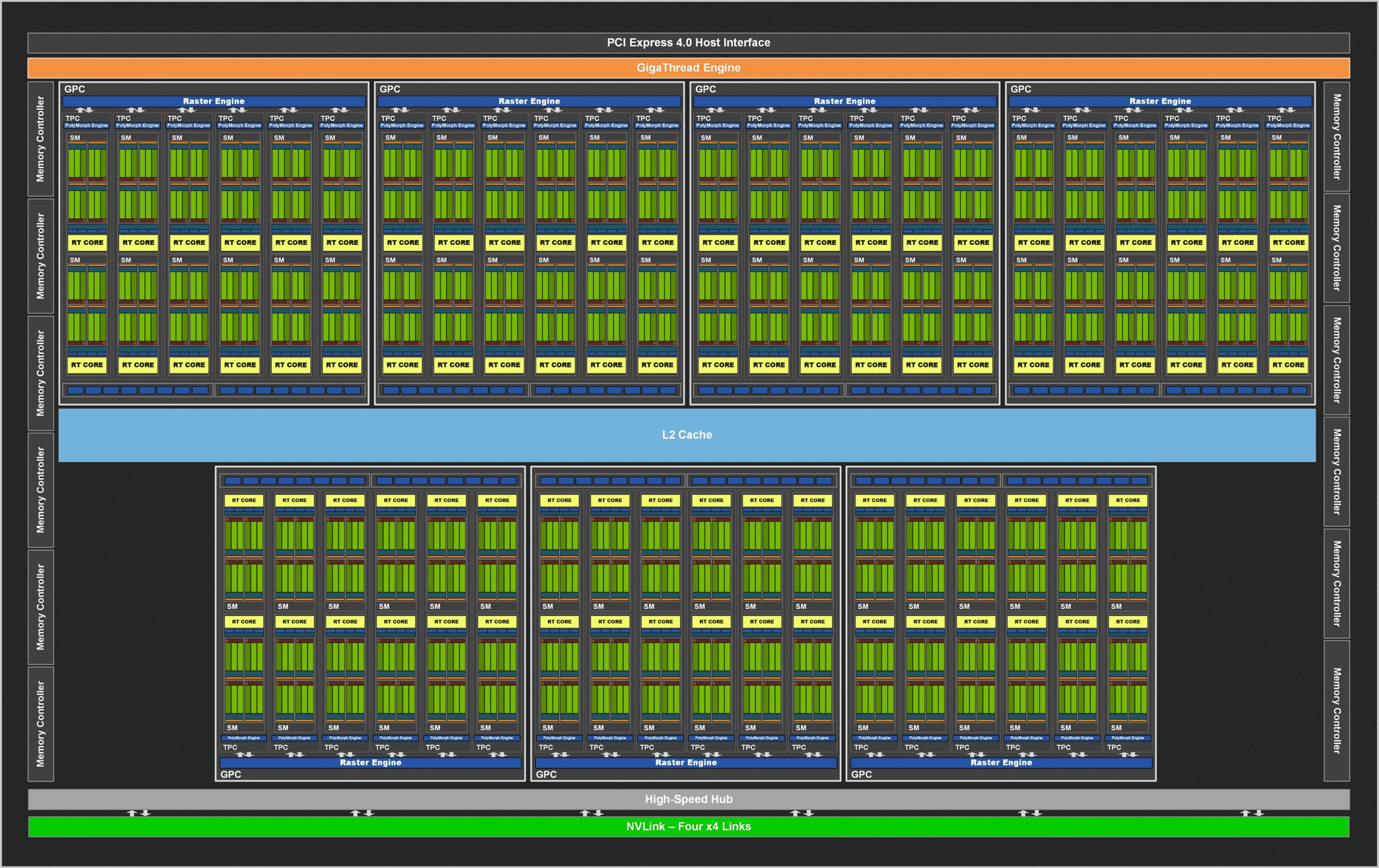
This additional 11% of transistors per square millimeter is why RDNA2 performs as well as it does in rasterization relative to Ampere even though Ampere has more transistors overall; the entirety of Ampere's 28.3 billion transistors cannot be used exclusively for rasterization since many of them comprise RT Cores and Tensor Cores that exclusively perform ray tracing and artificially intelligent upscaling, respectively. While the exact number of transistors that comprise RT Cores and Tensor Cores is not known, we can be sure that they amount to more than the difference in the overall number of transistors in RDNA2 and Ampere (28.3 billion - 26.8 billion = 1.5 billion) based on diagrams that illustrate the relative sizes of CUDA Cores, RT Cores, and Tensor Cores.

NVIDIA-Ampere-GA102-GPU-Block-Diagram.png


Hence, Ampere performs roughly as well as RDNA2 in rasterization with less transistors.

This indicates that RDNA2 isn't as efficiently designed as Ampere or - at the very least - isn't as efficiently put to use by AMD's drivers as Ampere is put to use by Nvidia's drivers. This assertion is based on rationale: an additional 11% of transistors should always result in better performance in rasterization (when other features are not enabled), but as AMD themselves showed at their announcement event, RDNA2 is faster than Ampere in rasterization only some of the time and is barely so whenever it is.

Hence, despite having more transistors per square millimeter and despite being able to use all of them for rasterization (whereas Ampere can use only some of its transistors for rasterization), RDNA2 is only as fast or slightly faster than Ampere in rasterization. Hence, RDNA2 isn't as impressive as it seems.

It can be argued that RDNA2 is indeed more efficient because it's performing as well as it is in rasterization relative to Ampere despite using less power; Navi 21 uses 300 watts at most at stock settings but GA102 uses 350 watts at most at stock settings. However, it must be considered that Navi 21 is - once again - manufactured on a smaller manufacturing process, that 300 watts is only 16.7% less than 300 watts, and that Navi 21 uses more transistors for rasterization (which naturally require less power since they don't have to function as fast as a lower number of transistors).

Hence, if Ampere were to be refreshed on TSMC's "7nm" manufacturing processes, it would be outright faster than RDNA2 in rasterization.
 

gspat

Member
Not really, because reduction in die size allows one of three things...

1 - Speed increase

2 - Power decrease

or

3 - A mix of both

The die size decrease isn't huge, so any of the above 3 options is really going to be minor.

At best, changing from Samsung to TSMC means moving to a more stable/reliable node with a better production yield.
 

geordiemp

Member
No.

The actual 6, 7 or 8 nm is just marketing, TSMC minimum FinFET gate width is 6 nm apparently, Samsung is likely same or close.

Note the actual metalisation layers are closer to 40 nm on both. So your density is incorrect. Samsung, TSMC and INtel wuill have similar densities.

Its likely EUV litho is only for critcal process steps around the gate to achieve such performance, the density improvements will come pver time when all layers are enhanced..

RDNA2 is about 3 things

  • New logic such as RT etc (bespoke on ps5 for mesh and VRS)

  • Faster frequencies and logic, which is a whole load of tech such as fine frequency gating, and reducing the silicon path distances - note all shader arrays on RDNA2 fast systems will have no more than 10 CU and optimsally laid out.
  • Data closer to where its needed - fast caches, shared caches, and if you look at the arrangement, less distance between cache and processing layout.
I seperated them as most posters think RDNA2 is about functions, the below slide says different


H4JovNm.png
 
Last edited:

Elias

Member
A smaller node performs as it's supposed to, that doesn't make amd's achievement any less impressive. And I suppose you think people who are gonna buy an Nvidia card are gonna shell out for another "refreshed" card?

Nvidia us better off taking their L with ampere and moving on to Hopper as soon as possible.
 
Last edited:

MadYarpen

Member
Hm from my perspective both companies have some products. And we can compare their performance. They are being released at the same time. So they are comparable regardless of the technical details, IMO ...

It's like with cpus. Intel is still behind with manufacturing nodes from what I understand, but they are releasing the best they have at the moment. Will we say they are actually better or more efficient than AMD if ryzen cpus are performing better?
 

BluRayHiDef

Banned
No.

The actual 6, 7 or 8 nm is just marketing, TSMC minimum FinFET gate width is 6 nm apparently, Samsung is likely same or close.

Note the actual metalisation layers are closer to 40 nm on both. So your density is incorrect. Samsung, TSMC and INtel wuill have similar densities.

Its likely EUV litho is only for critcal process steps around the gate to achieve such performance, the density improvements will come pver time when all layers are enhanced..

RDNA2 is about 3 things

  • New logic such as RT etc (bespoke on ps5 for mesh and VRS)

  • Faster frequencies and logic, which is a whole load of tech such as fine frequency gating, and reducing the silicon path distances - note all shader arrays on RDNA2 fast systems will have no moe than 10 CU and optimsally laid out.
  • Data closer to where its needed - fast caches, shared caches, and if you look at the arrangement, less distance between cache and processing layout.
I seperated them as most posters think RDNA2 is about functions, the below slide says different


H4JovNm.png

No, you're the one who's wrong. The number of transistors and the sizes of the dies for Navi 21 and GA102 are known facts. Hence, determining a rough estimte of the number of transistors per unit area is as simple as dividing the number of transistors by the total die sizes, as I did in the OP. Nothing you've said changes the fact that Navi 21 is 536mm^2 and has 26.8 billion transistors and that GA102 is 628.4mm^2 and has 28.3 billion transistors.

Math doesn't change.
 
Last edited:

geordiemp

Member
No, you're the one who's wrong. The number of transistors and the sizes of the dies for Navi 21 and GA102 are known facts. Hence, determining the number of transistors per unit area is as simple as dividing the number of transistors by the total die sizes, as I did in the OP. Nothing you've said changes the fact that Navi 21 is 536mm^2 and has 26.8 billion transistors and that GA102 is 628.4mm^2 and has 28.3 billion transistors.

Math doesn't change.

No its not that simple.

Not all transistors are same density, SRAM for example. Also faster frequencises and WGP gating will mean more spacing.

Here for your reference, and minimum metal pitch for metalisation is 40 nm or 400 angstroms. Dont get caught up in marketing and simple analysis. Note Intel has most density....its not about density, its more complex than that.


36qNeWk.png
 
Last edited:

gspat

Member
You're right!

Math doesn't change.

Nvidia's die is 17% larger with 5% more transistors.

Dropping the die size by changing vendor *might* change the size a bit, but probably not by much.
 

BluRayHiDef

Banned
I do not know if napkin-math will get you anywhere with that. There are also clocks, power-draw, latency and other aspects to consider.
Also that 128MB "infinity cache"- that costs die space too.

All the best,

I gave rough estimates of the transistor densities.
No its not that simple.

Not all transistors are same density, SRAM for example. Also faster frequencises and WGP gating will mean more spacing.

Here for your reference, and minimum metal pitch for metalisation is 40 nm or 400 angstroms. Dont get caught up in marketing and simple analysis.


36qNeWk.png
Okay, I concede defeat. However, though I may be wrong about transistor density, I'm still right about Ampere using less transistors for rasterization than RDNA2. So, my point still stands.
 

BluRayHiDef

Banned
Have to say, next to election meltdowns seeing the Nvidia fanboys trying to cope with RTX being 2nd rate (and still more expensive!) now has been the funniest!

Jm0PFkZ.gif

LOL, no one is coping about anything. I can buy a 6900XT if I want, but it has inferior ray tracing and currently doesn't have an equivalent to DLSS. Furthermore, it has less VRAM than its competitor, the RTX 3090. It's an inferior product, which is why it costs less.
 

geordiemp

Member
I gave rough estimates of the transistor densities.

Okay, I concede defeat. However, though I may be wrong about transistor density, I'm still right about Ampere using less transistors for rasterization than RDNA2. So, my point still stands.

All you can do is compare die size with performance, thats it - if AMD manage more performance on a smaller die then its more efficient design.

But thats not fair as Ampere has allot of die for ML and Ray tracing unique. So it is what it is, both will have advantages depending on workload..

And its more than densities, TSMC and Samsng will have their own secrets for special gate materials and steps in how to process them. Its not all the same.
 
Last edited:
I always bat for the underdog, which is why I really supported AMD over Intel, and was happy to see Ryzen do so well.
I am also really happy to see AMDs RDNA2 cards kinda close the gap.
And from a raster point of view they have caught up with Nvidia. They have also added RT, VRS and Mesh Shaders to match what Nvidia had, albeit a few years behind.

But unlike Intel, Nvidia continued to push tech even when AMD offered no competition to them.
AMD are still behind in RT, and are a long way behind in DLSS. Its going to take another couple of generations most likely for AMD to get where DLSS 2.1 is now, and who knows where Nvidia will be when AMD get to that point.

I am batting for AMD however, but Nvidia should get the respect they deserve.
 
Last edited:

gspat

Member
LOL, no one is coping about anything. I can buy a 6900XT if I want, but it has inferior ray tracing and currently doesn't have an equivalent to DLSS. Furthermore, it has less VRAM than its competitor, the RTX 3090. It's an inferior product, which is why it costs less.
I hope you completely enjoy your purchases.

I'm not entirely sure that AMD's RT is completely inferior. The tweets I've seen come out are definitely promising. Better FPS without using DLSS compared to having DLSS turned on in comparable GPUs makes it look as though it could be quite good!

I'm also looking forward to seeing what AMD brings forward to counter DLSS. Interesting times!
 

BluRayHiDef

Banned
All you can do is compare die size with performance, thats it - if AMD manage more performance on a smaller die then its more efficient design.

But thats not fair as Ampere has allot of die for ML and Ray tracing unique. So it is what it is, both will have advantages depending on workload..

And its more than densities, TSMC and Samsng will have their own secrets for special gate materials and steps in how to process them. Its not all the same.
So, you don't think that it's impressive that Ampere uses less transistors for equal performance in rasterization?
 

geordiemp

Member
So, you don't think that it's impressive that Ampere uses less transistors for equal performance in rasterization?

It is more about comparing the relative die sizes and what benefits they do, which I have not looked as I am ps5 next gen.

IF those transitor counts came from AMD and Nvidia then they will be correct, but they are 2 totally different arrangements so you can only compare die size and thats it.

I have not looked at respective die sizes for PC parts.

Infact you cant even compare die sizes, as AMD has allot of L3 cache to go for a smaller bus and lower spec memory so...

Maybe if you want to compare, you need to remove SOME of the infinty cache (120 mm2) as that is compensating for RAM speed and 256 bit bus.
 
Last edited:
I present to you OP's genuine desktop wallpaper:


55" screen. I sit two to three feet away from it.

W1i2pAn.jpg
 

Darius87

Member
I gave rough estimates of the transistor densities.

Okay, I concede defeat. However, though I may be wrong about transistor density, I'm still right about Ampere using less transistors for rasterization than RDNA2. So, my point still stands.
you can't just asume that's the case because RDNA2 also have RT and INT 4, 8 and it has more memory inside also Nvidia has more cuda cores then RDNA2 SP, don't know about ROPS? but anyway you're not right and whole OP doesn't make sense.
 

FireFly

Member
Okay, I concede defeat. However, though I may be wrong about transistor density, I'm still right about Ampere using less transistors for rasterization than RDNA2. So, my point still stands.
AMD sacrificed a lot of transistors for the 128 MB SRAM, in order to get more performance per watt. So if you're just interested in the shader architecture, it would be fairer to compare when both have the same bus type.

However AFAIK, AMD and Nvidia count transistors differently, so the best comparison would be die size when both are on the same process.
 
I present to you OP's genuine desktop wallpaper:


I'm a dickhead.
 
Last edited:

Elios83

Member
It really is impressive just for the fact that it closed a gap at the high end level.
No one thought they could compete with the 3090 RTX and here we are at a much more affordable price.
About ray tracing given that the feature is being already used on next gen consoles that have much weaker GPUs than these high end PC cards I think their implementation is just fine.
About DLSS they said they're developing their own solution, open platform as well.
 

thelastword

Banned
This entire post is woulda coulda shoulda.....

You minimize RDNA2's strengths to maximize what you think Ampere's strengths are......A bigger die is not necessarily better, it depends on the node. AMD should not be slighted for being on a better node. This is their third line of products on that node....Vega 7, Navi 1 and now Navi 2. Whatever NV chose to do with their node process was up to them, they had bigger coffers and have been the monopoly all this time...

Also, you are arguing for NV when you have no facts. How much space does the tensor and rt cores occupy on that die? You don't know. NV has been known to overhype everything, just as they did Ampere and many drank that coolaid. Hence "Will AMD even be able to compete with Ampere?" one naive juice drinker wrote on twitter......

For a while now Nvidia has been lowering IQ in their image on lower TF cards vs AMD for boosted framerates, that is without taking into all their dubious practices like gameworks, tesselation and PhysX...Add that and here is your superior rasterization performance on Nvidia in the past.....Now AMD has grown up and have the best CPU in the game, NV can no longer go to Intel and say "make our games play better with your cpu's, make the cpu footprint less on NV cards in DX 11". That's the reality of things more than nodes etc.....You think NV had lower power draw all this time because of how great their node was, no, it was because of all what they did at the driver level to lower IQ without you noticing it too much....

All of these monopolistic and underhanded methods where NV has not been transparent cannot affect AMD anymore, they are at pole position with their CPU's and now their GPU's. NV cannot approach them and say "gimp your GPU so it performs with your cpu". So when some folk think AMD is playing unfair to NV because of linking their GPU+CPU for better performance over the baby lamb Nvidia, I have to sigh.....

As for Ampere...NV has more transistors, they talk about rt cores and tensor cores, their die is bigger, yet you don't know how big they ore on the die. How future proof is that setup vs AMD's approach, perhaps that is the conversation we should be having. This is AMD's first foray into RT, it's also been a while since they targeted the high end and boom, they are already ahead in rasterization. From preliminary leaks, their RT is very good too and it looks to be more forward thinking in it's approach and scalability for future iterations. As opposed to NVidia, who will continue to produce bigger dies and say they've doubled the RT cores etc....in the foreseeable future...

NV are big boys, they chose their node, they chose their architecture. They work on marketing and hype to justify a high price as opposed to advancing the technology with good engineering that's beneficial to the whole industry. Their hype on 35.58TF was obvious to anyone versed in technology, double the rt cores did not offer double the performance vs Turing, putrid vram counts on such high TF cards. They hype, but within the hype are many shortcomings which they use to save money for the company, but take it out on customers by at least 300% overboard. A $1500 3090 and people will justify it and they know it. They sell their cards on a brute force ideal, but AMD has shown, GDDR6X (19gbps), we don't need that, lets works smarter, lets go with Inifinity cache. So technically we have more bandwidth at all resolutions and we can offer gamers enough Vram (16GB) for 4K and higher resolution textures as seen in DOOM.......Worse thing is to buy a 500-700 card with 8-10GB of Vram and are already limited in 1080, 1440p and 4k high texture gaming....

Architectures are more than TF and nodes.....I'd say AMD is already showing it's better architecture through their powerdraw at much less than Nvidia. If they match Nvidia's powerdraw, the performance gains will be even greater, much greater.....No AMD GPU has been OC'd yet. Yet all NV cards come OC'd, I'm talking about their FE cards and custom cards. No game has been developed for Radeon Rays yet, that we have seen, no game has been developed with Smart Access Memory yet. The rasterization performance will be even greater when the drivers mature in the next two months on older titles. So the truth is, Nvidia is in a world of hurt. If they were not. Having just sold you a 10GB $700 card, they would not be prepping 3060ti's, 3070ti and 3080ti's so soon......They know what they were doing, they knew, their vram count was too low, but they've been milking the same cows for so long at high prices, they released these cards to get as much money from blinded customers as possible. Now two weeks later they will offer a 3080ti for a much lower price with much more vram. Why? because they know how loyal some are to them in the industry, not because they've been pushing the envelope, but the great thing now is they have to react, because AMD is not effing around in the space anymore...
 
Better density means primarily smaller dies, cheaper dies, not "faster" dies.
The difference in size is more economical.

It's hard to chose which is better based on the amount of transistor, we don't know how many transistors are used for rasterization so this discussion is meaningless. When people discuss this on CPUs they have the exact numbers, how many transistors are being used to make a core and how much space it occupies inside the die.
We can't do this with neither RDNA2 or Ampere, and you seemed to forget, a lot os transistors on RDNA2 are just memory for the caches. Just the Infinity Cache alone going by the industry standards is estimated to be made of more than 6 billion transistors (which is more efficient now, huh?). And there's the Infinity Fabric there that also uses a good lot of transistors and the bigger improved media engine.
 
Last edited:

The Skull

Member
This is the kind of drivel hit piece I'd expect from Toms Hardware. I'd argue RDNA2 is more efficient. Smaller bus width and still trading blows at 4K? The Infinity Cache seems to be a great innovation. How about we spin this as Ampere isn't as efficient because it needs more bandwith and a bigger bus to keep up with RDNA2.
 

diffusionx

Gold Member
Let's see what the benchmarks say. Same thing as when people were calling out Nvidia's fake flop numbers (and that turned out to be correct). I was willing to buy Ryzen 1 even though it was still behind Intel's technology, simply because I didn't want to support Intel, but I am fine with Nvidia and buy GPUs strictly on performance. So AMD really has to deliver to get me to switch.
 
Last edited:

rnlval

Member
AMD sacrificed a lot of transistors for the 128 MB SRAM, in order to get more performance per watt. So if you're just interested in the shader architecture, it would be fairer to compare when both have the same bus type.

However AFAIK, AMD and Nvidia count transistors differently, so the best comparison would be die size when both are on the same process.
Well, BOM cost for RX 6800/6800 XT/6900 XT PCB is a mainstream 256-bit GDDR6 design.
 

adamosmaki

Member
so fucking what? can i buy an nvidia gpu for 650 with 11% better performance as you claim than a 6800xt? hell i cant even buy a 3080 for anything less than 1000 euros at the moment assuming i can actually find one. So as long as 6800xt is in stock and close to the msrp who gives a shit about manufacturing nodes?
 
  • Like
Reactions: GHG

BluRayHiDef

Banned
so fucking what? can i buy an nvidia gpu for 650 with 11% better performance as you claim than a 6800xt? hell i cant even buy a 3080 for anything less than 1000 euros at the moment assuming i can actually find one. So as long as 6800xt is in stock and close to the msrp who gives a shit about manufacturing nodes?

Then this thread isn't for you. Go to sandwich land and eat a sandwich or something.
 

sinnergy

Member
It’s quite impressive imo, they are coming in hard, contending Nvidia with lower price points . So what performance is lower, the prices also are
 
Last edited:

ReBurn

Gold Member
I don't understand the fascination with GPU features. The focus on technical buzzwords related to the quality of gaming in the upcoming generation is disappointing. Nobody seems to care whether these things are fun because everyone is too busy pissing their pants because the resolution is lower on some patch in the background in a still frame that you wouldn't look at while playing anyway.
 

FireFly

Member
Well, BOM cost for RX 6800/6800 XT/6900 XT PCB is a mainstream 256-bit GDDR6 design.
Sure, but I am talking about performance per mm/2 in comparison to Nvidia, not the overall cost. It's conceivable that by having a huge cache AMD are sacrificing performance per mm/2 for performance per watt, and maybe for a lower total cost overall.
 

Elias

Member
I don't understand the fascination with GPU features. The focus on technical buzzwords related to the quality of gaming in the upcoming generation is disappointing. Nobody seems to care whether these things are fun because everyone is too busy pissing their pants because the resolution is lower on some patch in the background in a still frame that you wouldn't look at while playing anyway.

Hardware features can't make a game "fun" but features like mesh shaders and vrs can improve fps which can make a gaming experience more enjoyable.
 
Top Bottom