llien
Member
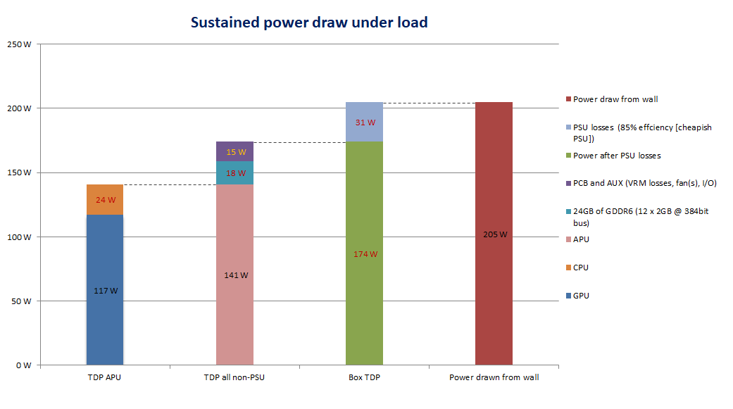
Welp, isnt 200w where unbearably loud PS4 Pro is?
If so, no, thanks.
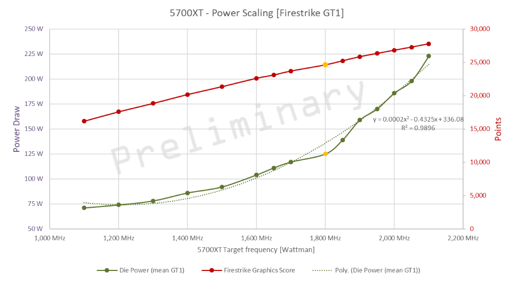
Betwen 5700 and XT looks like the most realistic bet.
Heck, which is quite a bump vs earlier hopes of betveen vega56 and 64.
And of course there is the spec arms race, so, perhaps, closer to XT.
And Im not buying the NotEnoughFor4k talk. It is about setings for the current gen, you CAN comfortably run most games at 4k on even non XT 5700.
And multiplier to be applied to the abstract next gen is highly arguable and Id argue that it is RT that will make a diference, potentially reducing raster load as the rastr tricks for shades and reflections could be done by RT instead.
If so, no, thanks.
Betwen 5700 and XT looks like the most realistic bet.
Heck, which is quite a bump vs earlier hopes of betveen vega56 and 64.
And of course there is the spec arms race, so, perhaps, closer to XT.
And Im not buying the NotEnoughFor4k talk. It is about setings for the current gen, you CAN comfortably run most games at 4k on even non XT 5700.
And multiplier to be applied to the abstract next gen is highly arguable and Id argue that it is RT that will make a diference, potentially reducing raster load as the rastr tricks for shades and reflections could be done by RT instead.
Last edited:


")