• Hey, guest user. Hope you're enjoying NeoGAF! Have you considered registering for an account? Come join us and add your take to the daily discourse.

The Curious Case of the Switch Foxconn Leak (Now a hardware fanfiction thread)

Luck has it, I don't rely on it. I believe it is a derivative of x1, it is custom and I'm wondering if the customization here is 16nm. I mean if it isn't, the entire design is sort of ridiculous imo, because you could make it passively cooled with eurogamer's clocks on 16nm.
Having a passive version immediately around the corner is the least ridiculous thing to expect. Nothing illogical about it being 20nm for cost reasons any more than it is for nvidia's own 2017 version.
 

Hermii

Member
Just expect that and be pleasantly surprised if it's 16nm. The answer is still: we don't know.


Not to mention Nvidia explicitly stated that the Switch uses a custom Tegra chip.

Actually their wording was "customized tegra", which could easily apply to a slightly altered x1.
 
Actually their wording was "customized tegra", which could easily apply to a slightly altered x1.

Sure but there are people out there convinced it's a completely standard TX1. I'd honestly be pretty surprised if it's essentially a TX1 with very, very minor alterations but that's still not a TX1.
 

Thraktor

Member
So a thought recently occurred to me regarding the supposed "enhancer" the Foxconn leaker talks about, and in particular that 12mm x 18mm chip being used in it. It's on the crackpot end of the spectrum, but I think I've firmly established my crackpot credentials in this thread already, so why not bring it up :p

My basic thought is, what if it's not a single 12x18mm die, but rather two smaller dies packaged closely together?

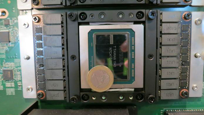
Bear with me on this. Last year I noticed a tidbit in a blog report of one of TSMC's symposia which confirmed that Nvidia "has a part in production with a logic chip and a four-die HBM stack", using TSMC's InFO multi-die packaging. This doesn't make a lot of sense for a desktop GPU (they could achieve the same results at lower cost with GDDR5), but may make sense for a mobile part where high bandwidth is required but GDDR5 is ruled out due to power draw (or space).

What occurred to me is that HBM2 dies are typically packed so closely to the logic die that they could easily be mistaken for a single die to someone who wasn't looking very closely. Have a look at this photo of Nvidia's GP100 package, with one (huge) GPU die and four HBM2 dies:

TP100_0GP1001.jpg


There's almost no gap between the GPU and HBM dies, and this gap could conceivably be even smaller with InFO packaging. The interesting thing is the dimensions of HBM2 dies, which are 7.75 mm × 11.87 mm. That is, they're pretty much exactly the same length as the chip reported to be used in the "enhancer". A logic die measuring approximately 10mm x 12mm side-by-side with a HBM2 die would look a lot like a single 18mm x 12mm die unless you got very close, and so, in theory, it's possible that this could be what the leaker saw.

Of course, it presents a lot of questions. Most notably, what is this 10x12mm die? Is it a GPU or an SoC? Why does it also apparently have 4GB of (presumably) LPDDR4 attached? If it does attach to Switch, would developers actually have to manage three different 4GB pools of RAM? If the regular Switch SoC can get by with 25.6GB/s, would Nintendo really feel they need 10 times that for the "enhancer"?

I'd still bet on the "enhancer" chip being a standard GP106, and Nvidia's HBM2-sporting mobile chip being Xavier, but I thought it was worth mentioning, at the very least. The fact that the dimensions line up so well is interesting, but I can't think of what the 10x12 die would be or why it would need so much bandwidth compared to a (similarly sized) regular Switch SoC.
 
If the X1 in the Switch is somehow 16nm, yet you only get 2.5hrs in Zelda, then they really got problems... You'd better hope that the X1 in Switch is still 20nm and Nintendo and NVidia has some room to improve battery life in future revs.
 

Yo Knightmare

Neo Member
If the X1 in the Switch is somehow 16nm, yet you only get 2.5hrs in Zelda, then they really got problems... You'd better hope that the X1 in Switch is still 20nm and Nintendo and NVidia has some room to improve battery life in future revs.
Code has a lot to do with that. Humor me here, but Zelda has been in dev for a while. It was built for a completely different architecture and different design paradigm. The switch could be muscling its way through.
 

McMilhouse

Neo Member
If the X1 in the Switch is somehow 16nm, yet you only get 2.5hrs in Zelda, then they really got problems... You'd better hope that the X1 in Switch is still 20nm and Nintendo and NVidia has some room to improve battery life in future revs.

The real question is how many months until there is a 16nm or 10nm The New Switch
 
Code has a lot to do with that. Humor me here, but Zelda has been in dev for a while. It was built for a completely different architecture and different design paradigm. The switch could be muscling its way through.
Nah. Sounds like wishful thinking because Nintendo would want people to know that we can expect better battery life on future titles.
 

Schnozberry

Member
The new one does perform slightly better in benchmarks, but we do not know why.

It could come down to newer version of android when the benchmark was taken.

Drivers and improvements to direct hardware access in Android, essentially. Android's software approach means we've never really seen what the X1 can do.
 
If the X1 in the Switch is somehow 16nm, yet you only get 2.5hrs in Zelda, then they really got problems... You'd better hope that the X1 in Switch is still 20nm and Nintendo and NVidia has some room to improve battery life in future revs.

We're getting at least 3 hours though, and that's the 25% upclock, I believe?
 
Late 2018 at the earliest for an X1 process shrink is my guess.

I saw your post in the other thread that you talked to a NVidia engineer. From how things were going, it is a surprise that the X1 in the new Shield is basically the same as the original. It is still a nice tidbit, so thanks for sharing that.

While I still suspect that some hardware changes were made aside from taking out the stuff Nintendo didn't want, I'm also starting to believe we were too focused on the physical hardware changes. Most of the development work was likely with the API and software tools.

Drivers and improvements to direct hardware access in Android, essentially. Android's software approach means we've never really seen what the X1 can do.

Interesting. How much higher are the new Shield's benchmarks compared to the original? Is it expected for the docked Switch to outperform the Shield in graphcal ability despite it being locked at a lower speed due to the API customization and (hopefully) lighter OS overhead?
 

Hermii

Member
Interesting. How much higher are the new Shield's benchmarks compared to the original? Is it expected for the docked Switch to outperform the Shield in graphcal ability despite it being locked at a lower speed due to the API customization and (hopefully) lighter OS overhead?
Well yea. I don't think anything on the shield comes close to MK8 at 1080p60 and that's a port.
 

Donnie

Member
2hr 25m was figure from a battery test with full screen brightness and wifi on, while just forcing the game to not go into sleep was the test I'm quoting. They weren't playing the game actively.

Ohers claim 3 hours. Could very well depend on wether the JoyCons are fully charged before going handheld.

I'm really not bothered about battery life though as long as it's over 2 hours. This is a console you take on the go after all. It sits in the dock and charges automatically so should always be full. If I take it out I can't imagine ever needing it to last more than 2 hours before I get home and pop it back on its dock.

IGN sez joycons don't suck off juice from main unit. In any case, 100% brightness is a huge battery killer. Lowering it to 50% or so probably buys that additional 30 minutes.
 

Donnie

Member
IGN sez joycons don't suck off juice from main unit. In any case, 100% brightness is a huge battery killer. Lowering it to 50% or so probably buys that additional 30 minutes.

Yeah what I'm referring to is the reports that the Switch itself can be kept alive by the JoyCons batteries.

As far as I remember people claiming 3 hours were using max settings. Which is why I wonder if JoyCon charging is the difference here.
 
So this could make an interesting upgrade down the line. http://www.anandtech.com/show/11185/nvidia-announces-jetson-tx2-parker

Interesting, I recall a bunch of people saying that A57s on a 16nm node makes no sense, yet this is what the Jetson TX2 has. Given the very rough power consumption numbers we have, I think we determined that 16nm with A57s would match the Switch's power consumption better than any other scenario, though that again is rough and without a good understanding of the RAM power consumption.
 
Top Bottom