If you look on the AMD road map you're notice the 2 key points of Navi is Scalability & Nexgen Memory , some people took Nexgen Memory to mean that it's going to be using GDDR6 but this is actually about the GPU having a NUMA architecture
https://www.amd.com/system/files/2018-03/AMD-Optimizes-EPYC-Memory-With-NUMA.pdf
https://hps.ece.utexas.edu/people/ebrahimi/pub/milic_micro17.pdf

Also Nvidia is also doing the same thing
MCM-GPU: Multi-Chip-Module GPUs for Continued Performance Scalability
https://research.nvidia.com/publication/2017-06_MCM-GPU:-Multi-Chip-Module-GPUs
What is Non-Uniform Memory Access (NUMA)? A multiprocessing (multi-die) architecture in which each processor is attached to its own local memory (called a NUMA domain) but can also access memory attached to another processor. It is called “non-uniform” because a memory access to the local memory has lower latency (memory in its NUMA domain) than when it needs to access memory attached to another processor’s NUMA domain. The advantage of this architecture is that it provides multiprocessor scalability, adds more memory bandwidth with the addition of more processor, and reduces the memory contention for CPUs if they are competing for access across a common bus (shared front-side bus).
https://www.amd.com/system/files/2018-03/AMD-Optimizes-EPYC-Memory-With-NUMA.pdf
ABSTRACT GPUs achieve high throughput and power efficiency by employing many small single instruction multiple thread (SIMT) cores. To minimize scheduling logic and performance variance they utilize a uniform memory system and leverage strong data parallelism exposed via the programming model. With Moore’s law slowing, for GPUs to continue scaling performance (which largely depends on SIMT core count) they are likely to embrace multi-socket designs where transistors are more readily available. However when moving to such designs, maintaining the illusion of a uniform memory system is increasingly difficult. In this work we investigate multi-socket non-uniform memory access (NUMA) GPU designs and show that significant changes are needed to both the GPU interconnect and cache architectures to achieve performance scalability. We show that application phase effects can be exploited allowing GPU sockets to dynamically optimize their individual interconnect and cache policies, minimizing the impact of NUMA effects. Our NUMA-aware GPU outperforms a single GPU by 1.5×, 2.3×, and 3.2× while achieving 89%, 84%, and 76% of theoretical application scalability in 2, 4, and 8 sockets designs respectively. Implementable today, NUMA-aware multi-socket GPUs may be a promising candidate for scaling GPU performance beyond a single socket
https://hps.ece.utexas.edu/people/ebrahimi/pub/milic_micro17.pdf
Also Nvidia is also doing the same thing
MCM-GPU: Multi-Chip-Module GPUs for Continued Performance Scalability
ABSTRACT Historically, improvements in GPU-based high performance computing have been tightly coupled to transistor scaling. As Moore’s law slows down, and the number of transistors per die no longer grows at historical rates, the performance curve of single monolithic GPUs will ultimately plateau. However, the need for higher performing GPUs continues to exist in many domains. To address this need, in this paper we demonstrate that package-level integration of multiple GPU modules to build larger logical GPUs can enable continuous performance scaling beyond Moore’s law. Specifically, we propose partitioning GPUs into easily manufacturable basic GPU Modules (GPMs), and integrating them on package using high bandwidth and power efficient signaling technologies. We lay out the details and evaluate the feasibility of a basic Multi-Chip-Module GPU (MCMGPU) design. We then propose three architectural optimizations that significantly improve GPM data locality and minimize the sensitivity on inter-GPM bandwidth. Our evaluation shows that the optimized MCM-GPU achieves 22.8% speedup and 5x inter-GPM bandwidth reduction when compared to the basic MCM-GPU architecture. Most importantly, the optimized MCM-GPU design is 45.5% faster than the largest implementable monolithic GPU, and performs within 10% of a hypothetical (and unbuildable) monolithic GPU. Lastly we show that our optimized MCM-GPU is 26.8% faster than an equally equipped Multi-GPU system with the same total number of SMs and DRAM bandwidth.
https://research.nvidia.com/publication/2017-06_MCM-GPU:-Multi-Chip-Module-GPUs
1 INTRODUCTION GPU-based compute acceleration is the main vehicle propelling the performance of high performance computing (HPC) systems [12, 17, 29], machine learning and data analytics applications in large-scale cloud installations, and personal computing devices [15, 17, 35, 47]. In such devices, each computing node or computing device typically consists of a CPU with one or more GPU accelerators. The path forward in any of these domains, either to exascale performance in HPC, or to human-level artificial intelligence using deep convolutional neural networks, relies on the ability to continuously scale GPU performance [29, 47]. As a result, in such systems, each GPU has the maximum possible transistor count at the most advanced technology node, and uses state-of-the-art memory technology [17]. Until recently, transistor scaling improved single GPU performance by increasing the Streaming Multiprocessor (SM) count between GPU generations. However, transistor scaling has dramatically slowed down and is expected to eventually come to an end [7, 8]. Furthermore, optic and manufacturing limitations constrain the reticle size which in turn constrains the maximum die size (e.g. ≈ 800mm2 [18, 48]). Moreover, very large dies have extremely low yield due to large numbers of irreparable manufacturing faults [31]. This increases the cost of large monolithic GPUs to undesirable levels. Consequently, these trends limit future scaling of single GPU performance and potentially bring it to a halt. An alternate approach to scaling performance without exceeding the maximum chip size relies on multiple GPUs connected on a PCB, such as the Tesla K10 and K80 [10]. However, as we show in this paper, it is hard to scale GPU workloads on such “multi-GPU” systems, even if they scale very well on a single GPU. This is due
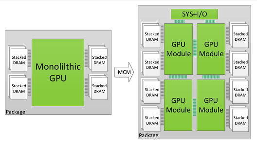
3 MULTI-CHIP-MODULE GPUS The proposed Multi-Chip Module GPU (MCM-GPU) architecture is based on aggregating multiple GPU modules (GPMs) within a single package, as opposed to today’s GPU architecture based on a single monolithic die. This enables scaling single GPU performance by increasing the number of transistors, DRAM, and I/O bandwidth per GPU. Figure 1 shows an example of an MCM-GPU architecture with four GPMs on a single package that potentially enables up to 4× the number of SMs (chip area) and 2× the memory bandwidth (edge size) compared to the largest GPU in production today.
3.2 MCM-GPU and GPM Architecture As discussed in Sections 1 and 2, moving forward beyond 128 SM counts will almost certainly require at least two GPMs in a GPU. Since smaller GPMs are significantly more cost-effective [31], in this paper we evaluate building a 256 SM GPU out of four GPMs of 64 SMs each. This way each GPM is configured very similarly to today’s biggest GPUs. Area-wise each GPM is expected to be 40% - 60% smaller than today’s biggest GPU assuming the process node shrinks to 10nm or 7nm. Each GPM consists of multiple SMs along with their private L1 caches. SMs are connected through the GPM-Xbar to a GPM memory subsystem comprising a local memory-side L2 cache and DRAM partition. The GPM-Xbar also provides connectivity to adjacent GPMs via on-package GRS [45] inter-GPM links. Figure 3 shows the high-level diagram of this 4-GPM MCMGPU. Such an MCM-GPU is expected to be equipped with 3TB/s of total DRAM bandwidth and 16MB of total L2 cache. All DRAM partitions provide a globally shared memory address space across all GPMs. Addresses are fine-grain interleaved across all physical DRAM partitions for maximum resource utilization. GPM-Xbars route memory accesses to the proper location (either the local or a remote L2 cache bank) based on the physical address. They also collectively provide a modular on-package ring or mesh interconnect network. Such organization provides spatial traffic locality among local SMs and memory partitions, and reduces on-package bandwidth requirements. Other network topologies are also possible especially with growing number of GPMs, but a full exploration of inter-GPM network topologies is outside the scope of this paper. The L2 cache is a memory-side cache, caching data only from its local DRAM partition. As such, there is only one location for each cache line, and no cache coherency is required across the L2 cache banks. In the baseline MCM-GPU architecture we employ a centralized CTA scheduler that schedules CTAs to MCM-GPU SMs globally in a round-robin manner as SMs become available for execution, as in the case of a typical monolithic GPU.
Last edited:
