Gosh, I hope its a 128 Bit Bus. 64 Bit would be a gigantic bottleneck. And also, 128 Bit would confirm 16nm, am I right?
Nope, it's completely independent of the SoC's manufacturing process.
Gosh, I hope its a 128 Bit Bus. 64 Bit would be a gigantic bottleneck. And also, 128 Bit would confirm 16nm, am I right?
Thats 100% definitely 531
Oh, yeah, I should have included that.
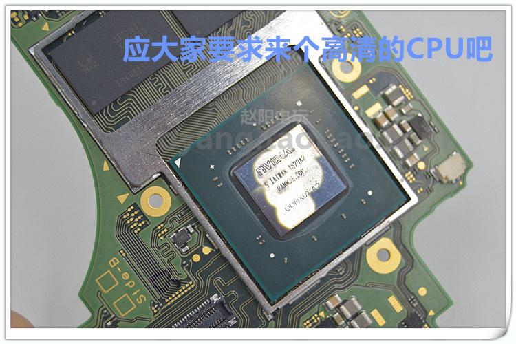
The SEC 531 chip pictured is K3RG4G40MM-MGCJ, which is 3GB, 3733 MT/s with a 64-bit interface, meaning a maximum total bandwidth of 59.5GB/s on a 128-bit bus.
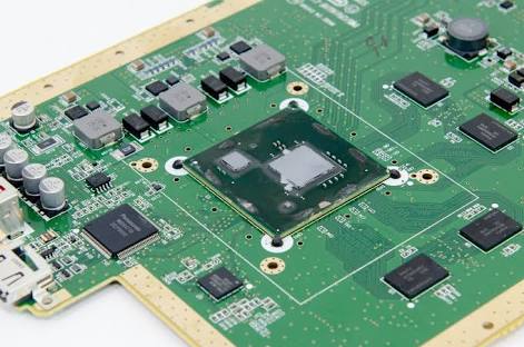
The 10x15mm chip is K4F6E304HB-MGCH, which is 2GB, 3200MT/s with a 32-bit interface, meaning a total of 25.6GB/s of bandwidth on a 64-bit bus.
Thats 100% definitely 531
Nope, it's completely independent of the SoC's manufacturing process.
was'nt the leaked docs said it had 25.6GB/s?
I suspect that may explain why there's the hole in the back of the dock here:

As well as a grill design above the presumable hub. Air is drawn in through those to the back of the Switch while docked.
Here is a Wii U for comparison

Oh, yeah, I should have included that.
The SEC 531 chip pictured is K3RG4G40MM-MGCJ, which is 3GB, 3733 MT/s with a 64-bit interface, meaning a maximum total bandwidth of 59.5GB/s on a 128-bit bus.
The 10x15mm chip is K4F6E304HB-MGCH, which is 2GB, 3200MT/s with a 32-bit interface, meaning a total of 25.6GB/s of bandwidth on a 64-bit bus.
But this could imply a theoretical X2. Or X02 like it's stated on the chip.
Thats 100% definitely 531
Possibly. I assumed the vents over the port area were just air flow vents for passive cooling on the small board in there. That elongated hole however is interesting. Still wouldn't that mean the Switch pulls its air from the back of the system rather than then the bottom? I'm not worried as this things looks like a master engineering marvel for how they built the board and assembled everything, but I'm curious what the solution could be. Obviously we'll know once it's in our hands for sure.
I suspect that may explain why there's the hole in the back of the dock here:
As well as a grill design above the presumable hub. Air is drawn in through those to the back of the Switch while docked.
But this could imply a theoretical X2. Or X02 like it's stated on the chip.
Nintendo Ninjas in 3,2,1....At least its not atolen, right guys?? At worse Nintendo could cancel the Factories contract, that ain't bad.../s
Thats 100% definitely 531
The last 2 didgets on the second line which i think would be the 6th and 7th characters i think are 30 so looks like the second option os more likely
I guessed so. Some people were claiming that 128 Bit would confirm 16nm.
So right now it looks like the bus is 128 Bit? Awesome news if true.
Edit: 6 GB too? No way. That's too good to be true.
Nintendo Ninjas in 3,2,1....At least its not atolen, right guys?? At worse Nintendo could cancel the Factories contract, that ain't bad.../s
I'm actually heavily leaning towards 4GB & 25.6GB/s at the moment. I don't think the SEC number is all that relevant, it's the two lines beneath it which are the product code (their product codes are 14 digits long and split into two 7 digit lines on the modules).
If it is the 2GB module that I suspect it is, then the two lines would be as follows:
K4F6E30
4HBMGCH
This looks like a pretty good match for what we see on the chips. You can see on this image:
The last two digits of the first line look like 3 and 0, and the last digit of the second line looks like H, which all matches up with the 2GB module.
Yes, although those specs were from the original TX1-based dev-kits, so it's not impossible that it may have changed.
The last 2 didgets on the second line which i think would be the 6th and 7th characters i think are 30 so looks like the second option os more likely
Didn't the foxconn leak says a73's? How is that accurate?
Yeah, I think Thraktor had it there. The rollercoaster!
Okay, so if we're at this low memory bandwidth, then how exactly is this chip customized for Nintendo? We can see the product number indicates it is a different run than the stock chips.
This will require chip scans, won't it.
Yeah, I think Thraktor had it there. The rollercoaster!
Okay, so if we're at this low memory bandwidth, then how exactly is this chip customized for Nintendo? We can see the product number indicates it is a different run than the stock chips.
This will require chip scans, won't it.
It was a guess based on the clock he saw while running a stress test.Didn't the foxconn leak says a73's? How is that accurate?
That should be a given.Maybe there's a larger cache on chip .
So the foxconn leak is pretty accurate on all specs. Which means a 4g version and super dock is shipped to devs. I guess it has something to do wih VR.
That's right, product code is the second line mainly, with mostly packaging details / production batches spilling over the third line.I'm actually heavily leaning towards 4GB & 25.6GB/s at the moment. I don't think the SEC number is all that relevant, it's the two lines beneath it which are the product code (their product codes are 14 digits long and split into two 7 digit lines on the modules).
That's $90 ?


It's pretty wild that there's nearly no air inside. It's so densely designed.
That's $90 ?
One of the pics in the OP makes it pretty easy to pick out the last 4 characters as MCGH.
I counted 32 traces from the RAM to the SOC. For what that's worth.
I counted 32 traces from the RAM to the SOC. For what that's worth.
I'm actually heavily leaning towards 4GB & 25.6GB/s at the moment. I don't think the SEC number is all that relevant, it's the two lines beneath it which are the product code (their product codes are 14 digits long and split into two 7 digit lines on the modules).
If it is the 2GB module that I suspect it is, then the two lines would be as follows:
K4F6E30
4HBMGCH
This looks like a pretty good match for what we see on the chips. You can see on this image:
The last two digits of the first line look like 3 and 0, and the last digit of the second line looks like H, which all matches up with the 2GB module.
