frankie_baby
Member
Both are not using eDRAM. THe One uses eSRAM, the U uses eDRAM. eDRAM is 3x as dense, however it must refresh its cells and under 4MB has a higher latency.
well wii u might not be edram either, check bottom of the last page
Both are not using eDRAM. THe One uses eSRAM, the U uses eDRAM. eDRAM is 3x as dense, however it must refresh its cells and under 4MB has a higher latency.
I don't think that this is important to the ones programming the games. I mean, if they don't program on an extremely low level, the compiler should the work.Xbone-r (I'm gonna coin that now) is using x86, Wii U is using PowerPC.
Read what I posted a couple hours ago. According to Marcan, Wii U's eDRAM looks like it's pseudostatic. It probably has to be, if only for backwards compatibility. So no refresh cycles here - same latency as real SRAM.Both are not using eDRAM. THe One uses eSRAM, the U uses eDRAM. eDRAM is 3x as dense, however it must refresh its cells and under 4MB has a higher latency.
Quite the opposite.Your entire scenario is different than mine.
Its seems me and you have very different concepts of what "maxing" a system out is. By your logic, when Insomniac said Resistance maxed out the capabilities of the PS3 it was true. Then they come back and say they got 40% more performance with Ratchet and Clank and like 80% more performance with Resistance 2. So all of those games maxed out its system by your methods. Only the one that did the most did according to my concept of maxing out.
Of course, but that was not my point at all.Any game can reach "its limit" on a console. I can write 10 lines of code and use all the resource of system hardware. That is not maxing out the system, though. That is just using up all of resources. Maxing out means optimizing to the point where there is nothing more that you can get out of the hardware. It means using all of the hardware most advanced features to their highest potential
So your issue is that there is no slowdown?Nothing Nintendo releases ever does this. Any game that runs at 60 FPS can get could get double the performance at 30. If you never hit an instance of slowdown, then that means you were no where near peaking the limits of the hardware. Mario Galaxy left so much leeway that is could still maintain solid 60 FPS with the screen split. There is a difference between a game being/looking good and a game pushing a system. I like MG 2 but I know the hardware can do far more than that.
Not to be an ass, but I only heard you saying that, and I've been reading about this for years, AFAIK blu already covered it, it's not blocked via firmware per see, but via the video encoder chip.Also, ATI said the chip was HD capable, but Nintendo had it locked in the firmware. Even the PS2 and Xbox1 could output in HD. The PS2 output at 1080i in actual games and it only had 4 MB edram had a lower texture bandwith than the GC embedded 1T-SRAM. Nintendo could have unlocked the higher resolutions if they wanted to. They just didn't.
I'll look into that.One of the homebrew apps for the Wii allowed you to play "some" videos at 720p "Files with MPEG-2 TS video streams (typically HDTV recorded .ts files) with resolutions up to 1280x720 play correctly."
Or perhaps devs didn't brag as much as Factor 5.Also, you are missing the entirety of what I'm saying. The main point was that when Mario Galaxy achieved 60 FPS, it did it with a ton of leeway. Nintendo didn't even try to "push" the system. People are letting their opinion of the game itself prevent them from seeing it technically. You are viewing it as fans rather than analysts. Also, that was not "all" that i looked at or pointed out.
Lilke lostinblue, your concept of maxing out is completely different than mine. Your view seems to be emphatic, or based on your emotional view and the games appeal to you. What devs target is their business and completely irrelevant to what I'm talking about. How I feel about the game/hardware is irreverent.
Speaking purely in terms of what the hardware can possibly achieve, no game pushed the Wii anywhere near it optimal limits, ie. maxing it out by my concept. There were no games that used every stage of the TEV to its optimized limit or push out the highest level texture effects it could achieve. There were no games that pushed the polygon potential of the Wii to the highest achievable in a real world scenario like Rebel Strike(which did it at 60 FPS by the way). There were no games that optimized the Wii CPU to do physics/A.I. to the "best" of its capability. There were games that had these things, but they were far from optimal. By that metric, no game maxed out the Wii's capabilities.
 Nintendo never bragged about polygons per second or anything like that.
Read what I posted a couple hours ago. According to Marcan, Wii U's eDRAM looks like it's pseudostatic. It probably has to be, if only for backwards compatibility. So no refresh cycles here - same latency as real SRAM.
It could be 1T-SRAM though could it not? That is similar in density to eDRAM and faster. XBO uses 6T-SRAM.I did, I don't see that in his recent tweets anywhere, and his earlier tweets did say eDRAM.
In either case, the statement I was correcting would still be wrong, the One at least does not use eDRAM. eSRAM is confirmed for that one. And whatever the Wii U uses, it can't be eSRAM due to density, eSRAM is 3x as large per memory unit.
It could be 1T-SRAM though could it not? That is similar in density to eDRAM and faster. XBO uses 6T-SRAM.
I reckon there have been some changes in MoSys and 1T-SRAM patents.Some places do use 1T-SRAM and eDRAM interchangably, but Nintendo used to say 1T-SRAM for the Wii, and they said eDRAM specifically for the Wii U, why change the name if they were using the same thing? But more importantly, would we not know with everyone who has looked at the cells by now?
So now that it's confirmed that the Xbox One will use 3GB for the OS and 5GB for games, I've noticed that Nintendo could of upgraded the Wii U ram to 6GB and used 5GB for games and 1GB for the OS, or possibly even 5.5GB for the games and 500mb for the OS like they will be doing in the future and cutting the OS ram and adding it for the games.
I know this is the GPU thread but since there is no ram thread I might as well post this here.
They also could've put 8 GB of GDDR5 RAM in the Wii U. They didn't. Don't mean to come off as rude, but there really isn't much to discuss on that front.
They also could've put 8 GB of GDDR5 RAM in the Wii U. They didn't. Don't mean to come off as rude, but there really isn't much to discuss on that front.
I would rather have 6GB of DDR3 than 8GB of GDDR5. It would give better all around performance for multiple tasks. GDDR is only "meant" for graphics.
If there was anything I would suggest Nintendo beefing up on the ram side, it would be the edram. If they had 100 MB of EDRAM, the rest would hardly even matter. Of course, that would put costs through the roof.
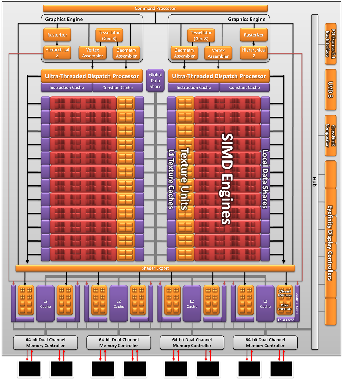
I'm still very intrigued by all those dual blocks in the GPU, and the fact that they're all congregated in the same general location. Seems like everyone just gave up on them.
What are some of the most common components in Radeon GPUs that would most likely occupy dual blocks? The only thing I'm aware of are geometry engines(this could allow Latte to achieved 2 polys/clk right?).
What else? Customized CUs? Tesselltors? (is more than 1 even necessary?) Also, do their sizes offer any clues to their functions? What about location? Closer to eDRAM, closer to shader cores, etc.
Nintendo could have done any number of things. What is there to discuss in what you posted?So now that it's confirmed that the Xbox One will use 3GB for the OS and 5GB for games, I've noticed that Nintendo could of upgraded the Wii U ram to 6GB and used 5GB for games and 1GB for the OS, or possibly even 5.5GB for the games and 500mb for the OS like they will be doing in the future and cutting the OS ram and adding it for the games.
I know this is the GPU thread but since there is no ram thread I might as well post this here.
I mean if they knew about Microsoft's spec plans for Xbox One.
Not saying Nintendo would do it but it is a interesting theory in my opinion.
I would rather have 6GB of DDR3 than 8GB of GDDR5. It would give better all around performance for multiple tasks. GDDR is only "meant" for graphics.
If there was anything I would suggest Nintendo beefing up on the ram side, it would be the edram. If they had 100 MB of EDRAM, the rest would hardly even matter. Of course, that would put costs through the roof.
What theory? Why would they put in so much more RAM whilst leaving the rest of the system untouched?
You'd rather have slower RAM and 2GB less of it due to a slight latency advantage? It might help the CPU out a bit, but what about the 4GB of data (or more) bound for the GPU? I think it's telling that devs were saying that a 4GB unified pool of GDDR5 would have been preferable or just as good as MS's solution. If DDR3 gave better performance for gaming purposes Sony would be using it and there wouldn't be move engines in the new Xbox.
PPC and x86_64 are different ISAs. You need to either emulate one via the other (translate ops on the fly), or pre-translate binary code from one to the other (which is what 360 did with xbox OG emulation), but in either case you need to handle endianness (the ordering of bytes in longer types). Neither of those is trivial. Pre-translation would be more viable, but in xb1's case, I'm highly skeptical whether Jaguar could quite hit the peek single-thread performance of Xenon's SIMD. So even if they did pre-translation, chances are they'd hit performance hurdles.But, (query for the technically inclined) if the difference between PPC and x86 was trivial though, then wouldn't we see some form of BC on the XBO?
Got it, thought krizz was just talking in general, like those people who claim that the use of GDDR5 in the PS4 will disadvantage it due to latency concerns. Although, I'd phrase it like this: the Wii-U and XB1 have slow main RAM, so they have to use eDRAM, whereas the PS4 and PC GPUs use GDDR5 and thus have no such concerns. That said, 6GB of any RAM in the Wii-U would be overkill and unbalanced from a system design perspective.It's all a matter of costs and design paradigms. WiiU and XB1 have 32MB of eDRAM, so the use of relatively slow DDR3 makes sense for the main RAM. PS4 doesn't have eDRAM, so they have to use fast GDDR5 as main RAM.
Therefore eDRAM + GDDR5 would be overkill.
You'd rather have slower RAM and 2GB less of it due to a slight latency advantage? It might help the CPU out a bit, but what about the 4GB of data (or more) bound for the GPU? I think it's telling that devs were saying that a 4GB unified pool of GDDR5 would have been preferable or just as good as MS's solution. If DDR3 gave better performance for gaming purposes Sony would be using it and there wouldn't be move engines in the new Xbox.
Got it, thought krizz was just talking in general, like those people who claim that the use of GDDR5 in the PS4 will disadvantage it due to latency concerns. Although, I'd phrase it like this: the Wii-U and XB1 have slow main RAM, so they have to use eDRAM, whereas the PS4 and PC GPUs use GDDR5 and thus have no such concerns. That said, 6GB of any RAM in the Wii-U would be overkill and unbalanced from a system design perspective.
Definitely. I wonder if Nintendo would have gone with 4GB if they would have known that PS4/XB1 will have 8GB. They really could have built a not too far away machine from XB1 with a little more money spent on every unit (for example at least 2 more CPU cores). I hope they will continue with this architecture in the next gen, just blow it up. Would allow a mature OS also.
I imagine a CPU with 1+8 Enhanced Espresso cores (the one being the core with 2MB L2 cache) ~1,6GHz, GX3 GPU with ~2TF and 128MB of eDRAM built as SoC on a 20nm process (or smaller if available in mature state). 8GB DDR4 RAM @128 bit. Release in 2016.
I think its pretty clear when Nintendo were designing the Wii u they were expecting the other 2 to hit sooner and be lower specced, even mid last year the general assumption was on ps4 having only 2gb of ram
There is no scenario in which the Wii U2 would be performance-competitive with Xbone and PS4 where it still uses the ancient Gamecube -> Wii -> Wii U CPU design. It needs to be abandoned, period. There is no other alternative. Nintendo is using a super-clocked version of a CPU architecture which was contemporary with the Pentium II.
You could say the same about the AMD CPU architecture though. As blu mentioned earlier the IPC isn't too far off and definitely not in a different league from the Jaguar cores.
There absolutely isn't a reason they HAVE TO abandon this architecture.
Of course they could just use a die shrinked PS4 chip and give it a day, but they would have to alter engines, OS etc too in this case.
I guess they will weigh the alternatives too
The architectural difference between XBone and X360 was far more deep than just x86 vs PPC.But, (query for the technically inclined) if the difference between PPC and x86 was trivial though, then wouldn't we see some form of BC on the XBO?
I have poor knowledge of what AMD was up to since their contemporary to the Pentium II, the Athlon. But I can tell you what Intel has done since the Pentium II:
Pentium III (Katmai -> Coppermine -> Tualatin)
Pentium 4 (Willamette -> Northwood -> Prescott)
Pentium M/Core (Banias -> Dothan -> Yonah)
Core 2 Duo (Conroe -> Allendale -> Wolfdale)
Core 2 Quad (Kentsfield -> Yorkfield)
Core iSeries Gen 1 (Bloomfield -> Lynnfield)
Core iSeries Gen 2 (Sandy Bridge -> Ivy Bridge)
Core iSeries Gen Next (Haswell)
Intel has released a total of 7 or 8 (depending on how you relate these CPU families) new CPU designs since the heyday of PowerPC 750. There were a total of 4 completely new architectures in that timeframe (P4, PM, Core 2, and Core iSeries). Haswell is again an entirely new architecture, so that makes 5 new architectures. Anyone who claims that the IPC of PII is similar to the IPC of Haswell is ignorant or delusional. I wouldn't hesitate to claim that Haswell probably has 10x IPC that PII has, nevermind that Haswell also has 10x the clockspeed. 10x IPC and 10x clockspeed. Is Haswell really 100 times faster than PII was? Without a single doubt, I could say yes and mean it truthfully on computations which didn't need to touch main memory too much. Moore's Law is a tough bitch on old CPU designs.
Intel has released a total of 7 or 8 (depending on how you relate these CPU families) new CPU designs since the heyday of PowerPC 750. There were a total of 4 completely new architectures in that timeframe (P4, PM, Core 2, and Core iSeries). Haswell is again an entirely new architecture, so that makes 5 new architectures. Anyone who claims that the IPC of PII is similar to the IPC of Haswell is ignorant or delusional. I wouldn't hesitate to claim that Haswell probably has 10x IPC that PII has, nevermind that Haswell also has 10x the clockspeed. 10x IPC and 10x clockspeed. Is Haswell really 100 times faster than PII was? Without a single doubt, I could say yes and mean it truthfully on computations which didn't need to touch main memory too much. Moore's Law is a tough bitch on old CPU designs. Will a PC running Haswell actually be 100 times faster than an old Pentium II PC? No, of course not, because the whole rest of the PC is a factor in performance as well. But in terms of sheer computational grunt, Haswell being 100 times faster than PII is a good rough estimate.
As for IPC of Jaguar vs. Espresso, I don't think 10x is too unreasonable a guess there either. AMD has not kept pace with Intel on sheer IPC, especially after the Core iSeries. So let's pretend clock-for-clock Jaguar is about 75% of an Intel CPU. Jaguar is conservatively clocked at 1.6 ghz on Xbone and PS4 compared to maybe 1.2 ghz on Espresso. There are 4 Jaguar cores vs. 3 Espresso cores. So doing some back of the envelope match, it's reasonable to guess that Jaguar has roughly 13 times more sheer computational grunt than Espresso does, considering just the cores and ignoring everything else such as main memory and the whole rest of the machine.
Xbox 1 XCPU: 951.64 DMIPS @ 733 MHz
Pentium III: 1124.311 @ 866 MHz
GC Gekko: 1125 DMIPS @ 486 MHz
Wii Broadway: 1687.5 DMIPS @ 729 MHz
Pentium 4A: 1694.717 @ 2 GHz
PS3 Cell PPE: 1879.630 DMIPS @ 3.2 GHz (sans SPE, SPE's are not meant for dhrystones/general purpose code)
X360 Xenon: 1879.630 DMIPS*3 = 5638.90 DMIPS @ 3.2 GHz (each 3.2 GHz core performing the same as the PS3)
PowerPC G4: 2202.600 @ 1.25GHz
AMD Bobcat: 2662.5*2 = 5325 DMIPS @ 1 GHz
Wii U Espresso: 2877.32 DMIPS*3 = 8631.94 DMIPS @ 1.24 GHz (again, final performance taking into account 3 fully accessible cores)
Pentium4 3.2GHz: 3258.068
8 core Bobcat: 4260*8 = 34080 DMIPS @ 1.6 GHz (said CPU doesn't exist, but best case scenario Jaguar is supposed to perform only 20% better; that would be 5112 DMIPS per core, 40896 DMIPS for 8 cpu's, but it's probably somewhere in between; again, taking into account 6 fully accessible cores, rumours suggest 2 cores for OS or so)
1T-SRAM is a MoSys trademark, they are not using 1T-SRAM anymore. Renesas has its own proprietary solution these days. If it's standalone, Renesas apparently calls it LLDRAM.Some places do use 1T-SRAM and eDRAM interchangably, but Nintendo used to say 1T-SRAM for the Wii, and they said eDRAM specifically for the Wii U, why change the name if they were using the same thing? But more importantly, would we not know with everyone who has looked at the cells by now?
I said 1T-SRAM because it'd match the Wii and it looks like what I'd expect 1T-SRAM to look like, but take it with a grain of salt.
Either way, it has to match or exceed the Wii's 1T-SRAM in timings and performance, or else Wii mode wouldn't perform properly.
1T-SRAM is a MoSys trademark, they are not using 1T-SRAM anymore. Renesas has its own proprietary solution these days. If it's standalone, Renesas apparently calls it LLDRAM.
Also, Marcan looked at the cells, and wrote he thinks it looked like pseudostatic RAM. It's indeed one of his older tweets from February 5th.:
Come on now, it's not like Bobcat is this killer performance design. IMO had nintendo widened the paired singles (unlikely due to the level of register file alterations and the ISA implications) or just added a G4-era altivec block things would have been more than evened out with Jaguar. The rest is just a matter of number of cores.There is no scenario in which the Wii U2 would be performance-competitive with Xbone and PS4 where it still uses the ancient Gamecube -> Wii -> Wii U CPU design. It needs to be abandoned, period. There is no other alternative. Nintendo is using a super-clocked version of a CPU architecture which was contemporary with the Pentium II.
Yet somehow PCs have gotten CPUs with ever higher clockspeeds and ever higher demands for rapid access to large pools of system memory and in the end the latency disadvantage hasn't meant jack shit because of the sheer bandwidth advantage DDR3 has over DDR2 has over DDR.
Depending on just how Sony and MS implement the memory controllers of Xbone and PS4, the latency difference between the DDR3 in Xbone and the GDDR5 in PS4 might be as little as 2x. Which is basically nothing.
Meanwhile the PS4 can access the entire 8 GB pool of GDDR5 with a bandwidth of 170 GB/s. The Xbox accesses it's 8 GB pool of DDR3 at 68 GB/s and even the 32 MB of eSRAM can only be accessed at 106 GB/s
when it comes to sheer fillrate the PS4 absolutely murders the Xbone because of raw bandwidth and also more ROPs. We're looking at a situation where the PS4 has enough sheer GPU grunt and bandwidth that some games might be forced to use FXAA on the Xbone and be able to use MSAA on the PS4. That's how big the performance difference is.
I never considered Espresso to have Haswell level IPC, so doesn't Jaguar and you know it.
More like 4-5x more raw power.
IPC of Jaguar probably being 30% higher than of Espresso (we can't say for sure yet).
Wrong thread for these discussions here though.
The new Xbox is using Mosys 6T-SRAM for the embedded memory on the GPU. Which is what Nintendo used to use on the GC but the 1 transistor variant 1T-SRAM.
But that's because other technologies have adapted to offset the ever increasing latency of DDR memory. Why do you think modern CPUs have an absolute ton of cache. Why AMD and Intel both got rid of Northbridge/Memory controllers and integrated these into the CPU's die. Why PCI-E lanes are now fed directly into CPUs. Then you have other technologies DDR's pre fetch, interleaving via combining multiple memory channels, and unganged multi channel setups.
You're making it sound as if DDR3's latency is basically a non issue. Quite far from it. The industry has had to go balls out implementing many of the above technologies to combat it. Almost all of the above target latency and efficiency > bandwidth.
But these figures are meaningless. They're both theoretical peak figures, real world the performance of both would be far more dependant on:
Memory architecture used
How developers optimise and code their games
How good Sony and Microsoft's bare metal and APIs are
Take for example:
Two graphics cards both featuring 3GBs of GDDR5 of memory. The memory on both cards is 100% identical, twelve 256 megabyte GDDR5 chips, 384bit bus, and same clocks. So both cards have a theoretical peak bandwidth of lets say 240GB/s. Only difference between the two cards is the memory controller the respective card's GPUs run. The first PC's graphics card runs a memory controller featuring clamshell bus. Where as the second computer's GPU runs a single bus.
The first card with its clamshell bus would absolutely mop the floor with the second card. That's despite the physical memory on both cards being identical.
The above example just highlights how freaking important the memory architecture is, not just the chips that are running on it.
We don't yet know, and may never, what memory architecture the Xbox One is running but I wouldn't be as bold as you to start making claims as how close to PS4 etc it's going to be. Heck we don't even know the full memory architecture of the PS4. While we know the PS4 features a clamshell bus for its ram, that's not enough to paint any picture.
I agree something like this is very likely to be the case. But Microsoft could pull a hell of a lot out of a DDR3 configuration if it's memory architecture is efficient. Shared memory address space for CPU and GPU, GPU having direct bus to the CPU's cache, large on die cache for CPU, customisations to the chips themselves like increased register sizes, we don't know. If Microsoft pulled out stops like those just mentioned and all Sony did was go for a clamshell GDDR5, Microsoft's system would punch far harder then its specs on paper show.
Flipper offered <6.2ns sustained latency at 162MHz, 10.4GB/s texture bandwidth (512bit bus), 7.6GB/s framebuffer bandwidth (384bit bus).yeah i'm now completely agreeing that it is basically 1t-sram, it didn't make much sense to drop it all makes sense now
by the way do we have bandwidth and other specs for the wii's 1t-sram?
Flipper offered <6.2ns sustained latency at 162MHz, 10.4GB/s texture bandwidth, 7.6GB/s framebuffer bandwidth.
6.2ns at 162MHz is a 1 cycle latency! For the WiiU to emulate this latency, it has to have 1T-Sram or one equivalent memory.Flipper offered <6.2ns sustained latency at 162MHz, 10.4GB/s texture bandwidth, 7.6GB/s framebuffer bandwidth.
Yes, three distinct pools on individual busses. MEM1 was on a 64bit bus I believe, so that part was pretty slow in comparison: 2.7GB/s at 324MHz. Still very low latency of course.weren't the framebuffer and texture cache seperate to the main 1t-sram though?
I believe it just means that it'll never be more than 6.2ns - how could it be less? Still, it should be absolutely impossible to match this latency using anything other than SRAM or pseudostatic RAM. Also, at very low capacities, using PSRAM makes no sense anymore because of the complex logic required (which is quite a bit more complex than regular DRAM logic), so that would probably explain why the 1MB pool is SRAM now.6.2ns at 162MHz is a 1 cycle latency! For the WiiU to emulate this latency, it has to have 1T-Sram or one equivalent memory.
About SRam sustained latency... is it possible to go lower than 1 cycle?
that explains over a billion and a half of Microsoft's transistors then, no wonder its such a huge chip
Plus the GCN GPU family got up to 4.6 ish billion transistors on its own, even with Microsofts cut down version it's probably around 4 billion, plus eight CPU cores. That is one big chip. I wonder how many transistors are in the Sony APU, but maybe it's not so different since MS used some for eSRAM while Sony went for more GPU resources.
I guess I wasn't very clear there. Yes, you're right that increasing latency going from DDR -> DD2 -> DDR3 required both Intel and AMD to adapt their designs to account for it. That said, I shouldn't also fail to mention that for a time in the mid-2000's AMD's CPUs had a cache size advantage over Intel's, AMD was using on-die memory controller while Intel still was on Northbridge, and for awhile there Intel was using MCMs of 2 modules with 2 cores each when AMD had all 4 cores on the same die! And yet, latency just wasn't that much of a killer in the days of Core 2 vs. Phenom. Latency ended up being really low on the list of problems that Intel cared about and rightfully so, they were eating AMD alive anyways in performance.
So far, we've heard more about PS4's optimizations for GPGPU than anything else. Anyways, AMD designed both SoCs for Xbone and PS4, I'm finding it hard to believe that they could have dramatically different memory architectures. AMD has been to hell and back on the GPU side in terms of bad bus design, anybody remember the "ring bus" on the R520 series? They would certainly be using their best available designs for both MS and Sony.
Judging from what has been said so far, it sounds like Sony did more customization than MS did. Neither you nor I can really speculate much on this not knowing what's inside, though I'm sure the 32 MB of eSRAM has all kinds of interesting connections with the rest of the SoC in Xbone. Whether the extremely low latency of the eSRAM allows operations which offset the bandwidth disadvantage, who knows. It's still a huge bandwidth difference no matter how you optimize memory architecture.
Should't it be 137.5GB/s? And no, I don't think you are. But the macros don't necessarily need to be accessible all at once. There could be a DDR-style bus protocol which allows multiple slower macros to masquerade as a single fast device. Say, if there were 8 macros at 225MHz each, you could have a 1024bit bus running at 550MHz. As re the actual macros count - I've got no idea.Looking through Renesas' docs again, Latte's MEM1 looks like it's using eight 128Kw * 256b macros. Shouldn't it therefore be on a 2048bit bus? 131GB/s? That doesn't seem right. Am I stupid or something?
One thing struck me. If the main cause of the slow OS is flash memory, it would be easy for Nintendo down the line to release a version with faster flash memory and faster OS without affecting the rest of the system ?