• Hey, guest user. Hope you're enjoying NeoGAF! Have you considered registering for an account? Come join us and add your take to the daily discourse.

Pachter: PS5 to be a half step, release in 2019 with PS4 BC

Theonik

Member
PS3 started this route towards highly multi threaded code with CELL being nicely leveraged by first parties. That continues with jaguar + more granular GPU compute.

Legacy code-bases can take a very long time to appropriately re-architect for newer paradigms, and it's becoming quite rare for anyone to approach this from ground-up these days - eg. perhaps the youngest shipping "AAA" engine on the market, what was used in Division - is already 7+ years old.
Ultimately this is something middleware providers should tackle fastest, but it hasn't been the case historically either.
Legacy codebases aside, there is just many CPU tasks a game engine needs to perform that are not trivially parallelise-able. One shouldn't look at PS3 either seeing as most of the work handled by the SPEs is done in the GPU now, and was not really an ideal solution to begin with. (besides, PS3 games were largely single threaded as far as the main logic was concerned) Really, a better single threaded architecture is preferable to more parallelism as you can get much more out of it in the general case, then you can squeeze as much additional performance from parallelism as your use case allows
 

THE:MILKMAN

Member
Back when PS4 was going to have 2GB of GDDR5 it also had steamroller (or bulldozer ) CPU

What Matt said is much worse than Ubisoft making a schoolboy error in assuming a non-final dev kit was final spec. Besides Unity came out a year after launch so really no excuse even if AMD duped everyone.

From the leaks though there seems to have been only one dev kit sent out to (third party) devs that had 8 1.6GHz Bulldozer cores and six months later the SoC-based near final Jaguar dev kit came out.
 

Shin

Banned
Did AMD breach any contract by not delivering what Sony/MS expected CPU-wise?

I think this was the reason:

SIE chose AMD 's small power - saving CPU core Jaguar architecture for PS 4 series. However, this is different from the initial plan, and in the initial plan I was planning to become the "Steamroller" core of Bulldozer (bulldozer) system. And APU of Bulldozer core PS 4 was planned to be manufactured at 28 nm of GLOBALFOUNDRIES, not TSMC's 28 nm.

However, at the last minute GLOBALFOUNDRIES 'rise of 28 nm became suspicious, SIE and AMD were urged to change the plan in a hurry. As a result, we moved the foundry to TSMC, due to time and engineering constraints, the CPU core was changed to a Jaguar core that is synthesizable already on the TSMC process. The first PS4 architecture was supplemented by doubling the number of CPU cores to reduce the CPU core's ability to reduce it.

2020 would be better, they'll be able to run with Zen3 which offers more IPC than Zen2 (also Zen is 52% IPC more than Excavator, not 40%)
Anyone know if they dropped PlayStation Home patent or is it still live, I wonder if they killed it off because Jaguar was too weak.
They were making money on that IIRC and lots of it also, bringing that back with PSVR support could be big for them.
 
Console launch dates are set for early adopters and influencers. If you have the tech to make these people switch, the mainstream market will follow, eventually.

Sony is in a good position where they can do product life-cycle transition smoothly by having a fairly decent overlap between PS5 launch and PS4/Pro EoL. If they manage it properly, they get an early lead into the new gen, what will help them create the network effect needed to blunt competitor products, while they enjoy the benefits of having a huge installed PS4 base.
 

THE:MILKMAN

Member
Your thread there Shin got locked by a mod citing dubious rumours so I doubt it was legit.

I did read the translated article though and there was one glaring contradiction (last minute foundry change) by the author that makes me question the rest of the article.
 
Legacy codebases aside, there is just many CPU tasks a game engine needs to perform that are not trivially parallelise-able. One shouldn't look at PS3 either seeing as most of the work handled by the SPEs is done in the GPU now, and was not really an ideal solution to begin with. (besides, PS3 games were largely single threaded as far as the main logic was concerned) Really, a better single threaded architecture is preferable to more parallelism as you can get much more out of it in the general case, then you can squeeze as much additional performance from parallelism as your use case allows
Well, isn't NPC animation/logic (AC Unity) a parallelizable task to begin with?

Pretty sure AC Unity is DX11/GNMX on consoles. Doesn't sound optimal to me, even if we just take into account draw calls (lots of thems with so many NPCs). I'm glad MS moved DX11 into maintenance status on XBOX ONE X. The sooner it dies, the better for everyone involved.

Also, it's true that most PS3 games were single-threaded (because there was only 1 PPU and 1 thread was reserved by the OS IIRC, only 360 had 3 PPUs, so the lowest common denominator was the PS3 PPU), but that didn't stop ND from refactoring the entire TLOU engine/codebase towards multithreading to reach the 60fps goal on the PS4. Was it easy? Nope. Was it necessary for a 720p30 -> 1080p60 leap? Absolutely.

Brute force/Moore's law can only get you so far. Ryzen is probably is the last x86 CPU that had such a huge (+50%) IPC jump. Intel IPC has stagnated since 2011 (Sandy Bridge). There will be no free lunch from now on. Programmers need to get their shit together. We don't live in the Saturn era anymore where multi-core CPUs were considered exotic/arcane.

And yes, SPUs were the precursor of Compute Shaders/GPGPU, just like Cell was a proto-APU. People argued they were "useless" and look where we are now. Many games use compute shaders for post-processing effects/physics.
 

Shin

Banned
Your thread there Shin got locked by a mod citing dubious rumours so I doubt it was legit.

I did read the translated article though and there was one glaring contradiction (last minute foundry change) by the author that makes me question the rest of the article.

I think Google does a poor job at translating the article, there are some tidbits in there that no one else ever mentioned.
So I'm inclined to believe some of it, particularly Fab switching at the very end.
 
I think Google does a poor job at translating the article, there are some tidbits in there that no one else ever mentioned.
So I'm inclined to believe some of it, particularly Fab switching at the very end.
I found your thread very interesting TBH. Perhaps you could find a native Japanese speaker to translate it properly? Shame it got locked.

Lots of interesting tidbits in there, such as PS4 Pro having a "Tiger" (I assume Puma is the proper translation) CPU. Probably the same applies to XBOX ONE X (Jaguar Evolved = Puma).
 

THE:MILKMAN

Member
I found your thread very interesting TBH. Perhaps you could find a native Japanese speaker to translate it properly? Shame it got locked.

Lots of interesting tidbits in there, such as PS4 Pro having a "Tiger" (I assume Puma is the proper translation) CPU. Probably the same applies to XBOX ONE X (Jaguar Evolved = Puma).

Interesting that he states as fact that Pro has the evolved 'Tiger' (Puma) core yet Sony themselves list Pro has still having Jaguar in the spec sheet!
 

Shin

Banned
Interesting that he states as fact that Pro has the evolved 'Tiger' (Puma) core yet Sony themselves list Pro has still having Jaguar in the spec sheet!

Features from Puma probably, as I said a lot is lost in translation with that article, since it was locked let's leave it as is.
 
There's a rumor that early PS4 devkits had a quad-core FX (Bulldozer) processor @ 3.2 GHz and they had to switch to Jaguar because of manufacturing constraints (TSMC -> GF).

Then again, FX CPUs are nothing spectacular in the PC gaming space either.


You're preaching to the choir, man... tell that to people who still believe that PPC CPUs @ 3.2 GHz are faster than Jaguar. MHz myth is still a thing.

Back when PS4 was going to have 2GB of GDDR5 it also had steamroller (or bulldozer ) CPU

I believe Sony was originally evaluating a PS4 design that would have 4 steamroller cores (hence 4x Bulldozer cores in the early devkit), but later in the process they had to switch to Jaguars precisely because Steamroller wouldn't have been ready in time for a late 2013 launch.
 

RaijinFY

Member
I think this was the reason:


2020 would be better, they'll be able to run with Zen3 which offers more IPC than Zen2 (also Zen is 52% IPC more than Excavator, not 40%)
Anyone know if they dropped PlayStation Home patent or is it still live, I wonder if they killed it off because Jaguar was too weak.
They were making money on that IIRC and lots of it also, bringing that back with PSVR support could be big for them.

Good thing they avoided GloFlo (often called GloFail)...
 

c0de

Member
Those "2-4GB" were based on a rumor. For all I know devs made it quite clear back how much RAM THEY expected.

Best case scenario is FMPOV is 16 GB + some dedicated cheap memory for OS.

For all we know, 8 GB were added very late to the PS4. Microsoft designed their box to have 8 gb right from the beginning which explains their esram solution. But yes, devs said before how much ram they wanted (and still didn't get it).
 

Hairsplash

Member
Mark Cerney "said" (but don't quote me) in the eurogamer article that the ps5 would be a clean slate... but that does not mean NO BC. In would ge insane not to have BC on the ps5. (Unless it could drive a 2Kx2K VR headset at 120hz... and 4K at 60hz)

I was thinking that the new PS5 should have TWO ps4pro chip's with a Ryzen CPU with the ability to go to 3.2Ghz...and a SSD caching drive along with a HDD. (Games are run off of the SSD, and stored on the HDD... when the space on the SSD runs out, the oldest game on the SSD gets written over... because there is a copy on the HDD)

I do not trust ANYONE other than Mark Cerny to give predictions about the state of the PS5...
 
For all we know, 8 GB were added very late to the PS4. Microsoft designed their box to have 8 gb right from the beginning which explains their esram solution. But yes, devs said before how much ram they wanted (and still didn't get it).

And we all know how that turned out. Maybe - just maybe - Sony learned one or the other lesson back then.

And it is correct that 8 GB was a last minute decision, but as I said, Cerny gathered the feedback from some major developers to convince the board to support 8GB.
 

RoboPlato

I'd be in the dick
And we all know how that turned out. Maybe - just maybe - Sony learned one or the other lesson back then.

And it is correct that 8 GB was a last minute decision, but as I said, Cerny gathered the feedback from some major developers to convince the board to support 8GB.
He also said they leveraged some of Sony's business relationships in order to get priority for the first round of higher density RAM chips. It'll be interesting to see if they do anything like that again in regards to components. The success of the PS4 would probably make that easier too.
 

newbong95

Member
I believe Sony was originally evaluating a PS4 design that would have 4 steamroller cores (hence 4x Bulldozer cores in the early devkit), but later in the process they had to switch to Jaguars precisely because Steamroller wouldn't have been ready in time for a late 2013 launch.

yes ps4 had streamroller/excavator cores but it didnt happen because it wasn't designed with tsmc fab in mind unlike the jag cores . If they did go with excavator cores then we would get 12-14cu gpu rather than 18 cu .
 

jroc74

Phone reception is more important to me than human rights
He also said they leveraged some of Sony's business relationships in order to get priority for the first round of higher density RAM chips. It'll be interesting to see if they do anything like that again in regards to components. The success of the PS4 would probably make that easier too.

This is good to hear.

Some said these companies could leverage relationships for getting RAM at lower costs too.

I hope so...

One thing Sony has as a plus is its in similar or the same markets with Samsung and some other component makers.

A deal on Sony camera sensors for Ram from Samsung at cheaper prices...make it happen Sony.
 

onQ123

Member
yes ps4 had streamroller/excavator cores but it didnt happen because it wasn't designed with tsmc fab in mind unlike the jag cores . If they did go with excavator cores then we would get 12-14cu gpu rather than 18 cu .

But the specs that had the bulldozer CPU already had the 1.84TF GPU it was the memory that was lower back then not the CU count.
 

mrklaw

MrArseFace
Brute force/Moore's law can only get you so far. Ryzen is probably is the last x86 CPU that had such a huge (+50%) IPC jump. Intel IPC has stagnated since 2011 (Sandy Bridge). There will be no free lunch from now on. Programmers need to get their shit together. We don't live in the Saturn era anymore where multi-core CPUs were considered exotic/arcane.

And yes, SPUs were the precursor of Compute Shaders/GPGPU, just like Cell was a proto-APU. People argued they were "useless" and look where we are now. Many games use compute shaders for post-processing effects/physics.

I've always been a fan of CELL. People slagged it off for being an expensive failure but it was perhaps ahead of its time. MS had easier development with DX based Xboxes, but I do think Sony is benefitting from their experience with PS3 and especially with what their first party teams are capable of technically
 

sirronoh

Member
Mark Cerney "said" (but don't quote me) in the eurogamer article that the ps5 would be a clean slate... but that does not mean NO BC. In would ge insane not to have BC on the ps5. (Unless it could drive a 2Kx2K VR headset at 120hz... and 4K at 60hz)

I was thinking that the new PS5 should have TWO ps4pro chip's with a Ryzen CPU with the ability to go to 3.2Ghz...and a SSD caching drive along with a HDD. (Games are run off of the SSD, and stored on the HDD... when the space on the SSD runs out, the oldest game on the SSD gets written over... because there is a copy on the HDD)

I do not trust ANYONE other than Mark Cerny to give predictions about the state of the PS5...

Not to only point this comment out because it's a sentiment that's been shared numerous times throughout this thread but, given the well documented history of console development over the last 30 years, why are we still speculating on the plausibility of high-end components for new console hardware (that are more commonly associated with PCs) that, while offering higher performance, are going to drive up the costs of the hardware? I realize this is an enthusiast forum and I probably shouldn't even be asking this but the last several pages feels like such a disconnect between "hopes and dreams" and what we're actually likely to get.

Sure it would look great (if developers actually took full advantage of it) but it's hard to argue for 16, 20, 24 TF's when 1.8TF is already giving us games like Horizon, Spider-man, and God of War. I realize that's a simplified view of the tech but I think the larger point still stands which is: at what point is console performance good enough for the majority of the market? It just seems like, in all this discussion on theory, that the very reason why we use these consoles in the first place is getting overlooked -- the games.

Anyway, I don't want to spend too much on this. I think price, not high-end specs (or an arms race around them) should be the guiding goal for hardware development.
 

THE:MILKMAN

Member
And we all know how that turned out. Maybe - just maybe - Sony learned one or the other lesson back then.

And it is correct that 8 GB was a last minute decision, but as I said, Cerny gathered the feedback from some major developers to convince the board to support 8GB.

I don't read that as a last minute decision. It says 'it came down to the very final meeting regarding the architecture of the PS4'

The bold is key. I doubt they decided the architecture of PS4 say at the end of 2012 or early 2013! (last minute) I think more likely in 2009 or 2010 after talking to devs that decision/change was made. Another big reason could have been devs informing them the competition has 8GB from the off too.
 

newbong95

Member
Tim Sweeny predicted that for photorealism 40 Tfs of Gpu compute power is required . So with ps5 pro we will comfortably reach (if ps5 base is more than 10Tfs) that goal but then what is the point of the successor to ps5 pro and the arms race of graphics power? i mean what will drive ps6 ... and further products except VR ?
 

Shin

Banned
i mean what will drive ps6 ... and further products except VR ?

That is the point where we're hitting diminishing returns, we'll probably jump to 8K but that will take a long ass time in console space.
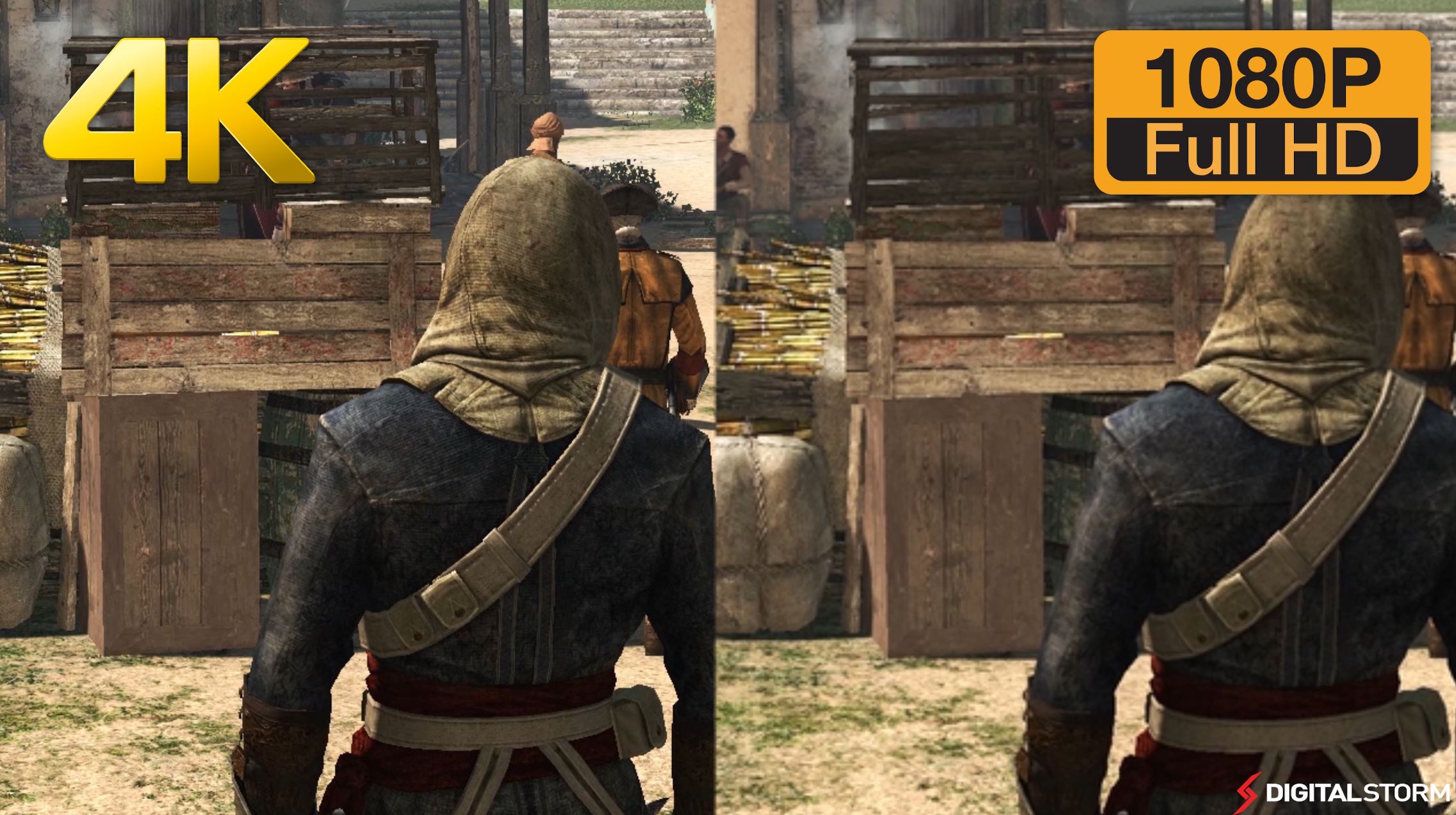
People saying 1.84TF and games looking great, I wonder how great it would look next to a native 4K game build from the ground up, I bet it would look blurry as hell.
They can very well hit $399 with a 10TF machine, not so great IMO but it would appeal to the masses just as they are satisfied with 1.84.
Therefor the option of a Pro model is certainly welcome for those that seek more power, as long as it's actually used and certain things are done at a system level.

Assassinscreed-4k-1080p-4.jpg
 

Marlenus

Member
Wait...What? This is going to need more explanation if I'm understanding this right! Sony and MS didn't know they were getting weak Jaguar cores on APUs they were helping design and customise with AMD?

Also Matt if I can ask.....Do you have any knowledge or insight into when 7nm will be ready because I'm really not confident 2019 can be met if that is the target right now.

GF are targeting their High Performance 7nm node to be available for Zen 2 next year which is why I think 2019 is doable.

Features from Puma probably, as I said a lot is lost in translation with that article, since it was locked let's leave it as is.

Puma and Jaguar are functionally the same. Puma just has layout optimisations to improve the power curve meaning a 2.0 Ghz Puma draws the same as a 1.8 Ghz Jaguar.

It was simply a power saving step with no architectural benefits.

Tim Sweeny predicted that for photorealism 40 Tfs of Gpu compute power is required . So with ps5 pro we will comfortably reach (if ps5 base is more than 10Tfs) that goal but then what is the point of the successor to ps5 pro and the arms race of graphics power? i mean what will drive ps6 ... and further products except VR ?

AI

do the die area consumed by jag and bulldozer cores same ? or overall bulldozer apu die size was more than the jag apu?

Jaguar is much smaller than bulldozer and much more power efficient.

The problem with Bulldozer is that the die and power consumption would both be higher making the box more expensive or coming with a smaller GPU and I guess the engineers decided that Jaguar + Pitcairn (essentially) was a better compromise than Bulldozer + something weaker.
 

Shin

Banned
Since we're discussing 4GB DDR4L/DDR3L for BG/OS tasks this is what Mark Cerny had to say about it.
This is a bad comparison but I am curious as to the implications it would have if the OS was running off a different pool.


In a new tech session this week, Cerny walked through more details of the PS4 Pro, including what the extra 1GB of DDR3 RAM is used for.

”We felt games needed a little more memory, about 10% more. So we added about a gigabyte of slow, conventional DRAM to the console," Cerny told Gamasutra. He continued by explaining that the PS4 Pro handles switching between applications (like Netflix) and a game differently, freeing up almost 1GB of 8GB GDDR5 RAM:

On the standard [PS4], if you're swapping between an application like Netflix and a game, Netflix is still resident in system memory, even when you're playing the game. We use that architecture because it allows for very quick swapping between applications. It's all already in memory.

On PS4 Pro, we do things a bit differently. When you stop using Netflix, we move it to the gigabyte of slow, conventional DRAM. Using that sort of strategy frees up almost a gigabyte of our 8GB of GDDR5. We use 512 megabytes [of that] for games, which is to say that the games can use 5.5GB rather than 5 GB. And we use most of the rest to make the PS4 Pro interface 4K, rather than the 1080p it's been to date. So when you hit the PS4 button, that's a 4K interface.

As Eurogamer explains it, the additional 1GB of RAM is used to swap out non-games apps from the 8GB of GDD5 RAM. 512MB is available to developers for 4K render targets and framebuffers, while another 512MB is used for handling a 4K version of the dynamic menu front-end.

According to Cerny's estimation, the PS4 Pro's 8GB of GDDR5 RAM has seen a roughly 24% frequency boost, and it now runs at around 218GB per second (standard PS4 is 176GB/s).
 

That's an area in gaming that could use some major improving, indeed. AI and AI-driven world simulation. With crazy amounts of memory they could theoretically hold a rather large number of AI entities permanently without resorting to statistical modelling, and boatloads of highly parallel GPU flops would enable deeper, fuzzier behavior/logic trees.
 
That's an area in gaming that could use some major improving, indeed. AI and AI-driven world simulation. With crazy amounts of memory they could theoretically hold a rather large number of AI entities permanently without resorting to statistical modelling, and boatloads of highly parallel GPU flops would enable deeper, fuzzier behavior/logic trees.

GPU?!?

I would of thought that the high data dependency would mean these types of workloads aren't so parallelizable, thus would be much better suited to CPUs.

I don't know of any game currently that does AI on the GPU.
 
That's an area in gaming that could use some major improving, indeed. AI and AI-driven world simulation. With crazy amounts of memory they could theoretically hold a rather large number of AI entities permanently without resorting to statistical modelling, and boatloads of highly parallel GPU flops would enable deeper, fuzzier behavior/logic trees.
That implies that AI pathfinding is GPGPU accelerated. Few companies do that AFAIK. Most companies would rather write generic CPU code for AI pathfinding, which is obviously too taxing for the Jaguar.

So, it's not a matter of power (flops), but a matter of technical expertise. It's not very different from the Cell SPU situation.

Btw, this technology is almost 1 decade old:

https://www.youtube.com/watch?v=bka2zm-vhms
http://s08.idav.ucdavis.edu/shopf-crowd-simulation-in-froblins.pdf

That's why I don't buy the "PS4 is too weak for AC Unity" mantra. PS4 GPU (semi-custom Radeon 7850/GCN 1.1 uArch) is leaps and bounds faster & more capable than a Radeon 4870 (VLIW5 uArch).

I don't know of any game currently that does AI on the GPU.
Uncharted 4 is one of them.

ND games on the PS3 used the SPUs for AI pathfinding.
 

THE:MILKMAN

Member
GF are targeting their High Performance 7nm node to be available for Zen 2 next year which is why I think 2019 is doable.

They don't have the best record of keeping to dates but two questions:

1, Sony have used TSMC for all PS4 chips I think (and PS3 before it?) Would they risk switching?

2, Have Sony ever launched a console on a brand new node before as it seems to be another risk to add to all the potential ones already in developing a console.

Would it not be wiser to launch on a already mature process?
 

Shin

Banned
Would it not be wiser to launch on a already mature process?

By 2019/2020 7nm would have already been mature, would they really want GloFo to manufacture the SoC then ship it to China.
When TSMC is ahead of GloFo and located in Taiwan along with all their Fabs, seems a stupid move that isn't cost efficient.

TSMC's 7nm Fin Field-Effect Transistor (FinFET) process technology provides the industry's most competitive logic density and sets the industry pace for 7nm process technology development by delivering 256Mb SRAM with double-digit yields in June 2016. Risk production started in April 2017.

We expect double digit customer product tape-out in 2017.

Compared to its 10nm FinFET process, TSMC's 7nm FinFET features 1.6X logic density, ~20% speed improvement, and ~40% power reduction. TSMC set another industry record by launching two separate 7nm FinFET tracks: one optimized for mobile applications, the other for high performance computing applications.

TSMC's 5nm Fin Field-Effect Transistor (FinFET) process technology is optimized for both mobile and high performance computing applications. It is scheduled to start risk production in the second quarter of 2019. Compared to its 7nm FinFET Plus process, TSMC's 5nm FinFET adopts EUV Lithography for more critical layers to reduce multi-pattern process complexity while achieving aggressive die area scaling.

From that you can make take away that TSMC won't be going with EUV for their 7nm process, I believe this is correct and reported by news outlet as well.
On the surface TSMC seems a lot smarter with how they are handling their business, their yields were healthy during risk production hence why the customer tapeouts I reckon.
That 5nm EUV is pretty much what we can expect in a PS5 Slim or Pro model, why risk money on 7nm EUV when 5nm isn't a big jump and there would be bigger gains there.
 
GPU?!?

I would of thought that the high data dependency would mean these types of workloads aren't so parallelizable, thus would be much better suited to CPUs.

As tapantaola mentioned, there are several algorithms that are optimized to be run in extremely parallel fashion that are vastly more efficient than your average A*/D*/MTS/etc. And that's not even getting into crazier stuff like genetic algos, machine learning, etc.

That implies that AI pathfinding is GPGPU accelerated. Few companies do that AFAIK.

Yup, few companies do it right now, but I believe they will gradually migrate towards more parallelized pipelines as linear, serial performance stagnates. At least I hope so, since it's, in my opinion, a better (as in, a more forward-thinking) way to do it.
 

Fafalada

Fafracer forever
Theonik said:
there is just many CPU tasks a game engine needs to perform that are not trivially parallelise-able.
Completely agree, but even there some of it goes back to the fact games have primarily evolved as serial-process applications, and have over 30 years of history as such.
More importantly though - it's not been the main source of bottlenecks this gen - DX9/11 renderer legacy on the other hand, has (and still is, in many shipping games 4 years in).

Really, a better single threaded architecture is preferable to more parallelism
All true - and also why current gen has been seen as an upgrade on CPU side by development community.
 
That is the point where we're hitting diminishing returns, we'll probably jump to 8K but that will take a long ass time in console space.
People saying 1.84TF and games looking great, I wonder how great it would look next to a native 4K game build from the ground up, I bet it would look blurry as hell.
They can very well hit $399 with a 10TF machine, not so great IMO but it would appeal to the masses just as they are satisfied with 1.84.
Therefor the option of a Pro model is certainly welcome for those that seek more power, as long as it's actually used and certain things are done at a system level.

Assassinscreed-4k-1080p-4.jpg

This looks accurate. 1080p looks extremely blurry on 4K TV after playing at 1440p or checkerboard 4K. The Witcher 3 is literally unplayable for me now after playing Horizon Zero Dawn. Waiting for that Pro patch.
 

truth411

Member
By 2019/2020 7nm would have already been mature, would they really want GloFo to manufacture the SoC then ship it to China.
When TSMC is ahead of GloFo and located in Taiwan along with all their Fabs, seems a stupid move that isn't cost efficient.


From that you can make take away that TSMC won't be going with EUV for their 7nm process, I believe this is correct and reported by news outlet as well.
On the surface TSMC seems a lot smarter with how they are handling their business, their yields were healthy during risk production hence why the customer tapeouts I reckon.
That 5nm EUV is pretty much what we can expect in a PS5 Slim or Pro model, why risk money on 7nm EUV when 5nm isn't a big jump and there would be bigger gains there.
Isn't TSMC 7nm more like 10nm?7nm+ is true 7nm. I rather have 7nm+. If the PS5 comes out in holiday 2020, there's no reason not to be based on 7nm+ chips.
 

truth411

Member
What would the difference in regards to the console itself if it's not "7nm+"?
Clocked higher? Density/more performance? I doubt the cost would be much different, it's more of a question of why not? Imo.

Edit: Also by that time it should also have Zen3.
 
Yeah but instead of $500 every 6-8 years many of us are now basically paying $400 every 3-4 years making the total cost $800 for the 6-8 year period instead on $500. Add the online subscription too which are now standard on all consoles and the $599 PS3 price everybody laughed at suddenly feel cheap.
Like I've said before, I want Crazy Ken back, the current baby steps consoles with budget PC parts couldn't be more boring. There are barely any surprises anymore, those with 1080ti's today are probably already playing the next gen of consoles.
If you factor in the YLOD/RROD fiasco, then $599 doesn't feel that "cheap" anymore, does it?

How many still have a launch PS3/XBOX 360? The majority had to buy a Slim model later on. That's $600 + $300 (PS3 Slim) = $900 and there's no performance increase like on PS4 Pro/XBOX ONE X.

The current paradigm trumps the "ticking bomb" consoles that we had last gen. You have to understand that companies strive to make mass appeal products (Nintendo Switch is a prime example of this), they don't care about the minority that cares that much about "exotic" technology. PS3 taught 'em a hard lesson.

64 ROPs sounds right. Would 256 bit give enough bandwidth to feed a 10-12TF GPU?

16GB seems low considering maybe 4+ GB reserved for OS. 32GB?
256-bit GDDR6 32GB (16 x 2GB chips) is the bare minimum I expect from a PS5. Lithography progress alone should easily quadruple memory density/capacity for roughly the same cost.

64GB HBM3 might be possible if they delay it until 2021-2022 and it would certainly give longevity until 2030.

128GB (the historical 16x RAM increase) doesn't seem very likely IMHO, especially considering the fact that next-gen optical media (BDXL) most likely won't exceed 100GB.

We won't get a pure SSD solution until PS6 at least, so I expect lots of RAM on the PS5 to mitigate streaming issues (PlayGo wizards will certainly have a field day at this).

I'd be more curious as what they do with DualShock 5, light bar disable option in OS since that was requested a lot.
Make it easier on developers like MS did with a FPS counter on the SDK and other shiznit?
Touchpad made of LCD with whatever info on it, clickable still and retain it's current features?

We should make our own general PS5 thread since people are interested in the subject.
There's a lot to cover even if it will be more of a wishlist, idea box/general discussion, sucks that developers and platform holders decide everything behind the screen.
DualShock 5 should have a 1080p screen and 5 GHz WiFi to enable flawless Remote Play. PS Vita and its crappy 2.4 GHz WiFi just doesn't cut it anymore.

If someone wants a cheaper option, DualShock 4 should still be supported (BC should also apply to accessories, not just games).

Do you think that PS5 could launch on existing tech i.e 16nm?
It might be possible with a discrete CPU/GPU setup.

The downside? $599 price tag, huge size (case/motherboard/cooler), poor thermals, YLOD might rear its ugly head once again.
 

Shin

Banned
Clocked higher? Density/more performance? I doubt the cost would be much different, it's more of a question of why not? Imo.

Edit: Also by that time it should also have Zen3.

I was hoping for a more thorough explanation :p
But good news since you asked that question I dug up an article from Anandtech, their 2nd gen 7nm process will use EUV.

Beyond 10 nm at TSMC: 7 nm DUV and 7 nm EUV
As noted previously, TSMC's 7 nm node will be used by tens of companies for hundreds of chips targeting different applications. Initially, the company plans to offer two versions of the manufacturing technology: one for high-performance, and one for mobile applications, both of which will use immersion lithography and DUV. Moreover, eventually TSMC intends to introduce a more advanced 7nm fabrication process that will use EUV for critical layers, taking a page from GlobalFoundries' book (which is set tp start 7 nm with DUV and then introduces second-gen 7 nm with EUV).

TSMC's first-generation CLN7FF will enter risk production in Q2 2017 and will be used for over a dozen of tape outs this year. It is expected that high-volume manufacturing (HVM) using the CLN7FF will commence in ~Q2 2018, so, the first ”7-nm" ICs will show up in commercial products in the second half of next year. When compared to the CLN16FF+, the CLN7FF will enable chip developers to shrink their die sizes by 70% (at the same transistor count), drop power consumption by 60% or increase frequency by 30% (at the same complexity).

The second-generation 7 nm from TSMC (CLN7FF+) will use EUV for select layers and will require developers to redesign EUV layers according to more aggressive rules. The improved routing density is expected to provide ~10-15-20% area reduction and enable higher performance and/or lower power consumption. In addition, production cycle of such chips will get shorter when compared to ICs made entirely using DUV tools. TSMC plans to start risk production of products using its CLN7FF+ in Q2 2018 and therefore expect HVM to begin in H2 2019.

bdb4501d6a.png


As it turns out, all three leading foundries (GlobalFoundries, Samsung Foundry and TSMC) all intend to start using EUV for select layers with their 7 nm nodes. While ASML and other EUV vendors need to solve a number of issues with the technology, it looks like it will be two years down the road before it will be used for commercial ICs. Of course, certain slips are possible, but looks like 2019 will be the year when EUV will be here. In fact, keeping in mind that both TSMC and Samsung are already talking about their second-gen EUV technologies (which they call 5 and 6 nm) that will use more EUV layers, it looks like the foundries are confident of the ASML TwinScan NXE manufacturing tools (as well as of the Cymer light source, pellicles, photoresists, etc.) they are going to use.
 
Top Bottom