-
Hey, guest user. Hope you're enjoying NeoGAF! Have you considered registering for an account? Come join us and add your take to the daily discourse.
You are using an out of date browser. It may not display this or other websites correctly.
You should upgrade or use an alternative browser.
You should upgrade or use an alternative browser.
- Status
- Not open for further replies.

LordOfChaos
Member
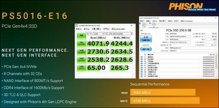
So this is actually a real PCI-E 4 PC SSD SSD controller, the PS5 part of the name is a funny little coincidence, would be funny if that was actually it out in the open. But I mean, also, PhiSon, 5
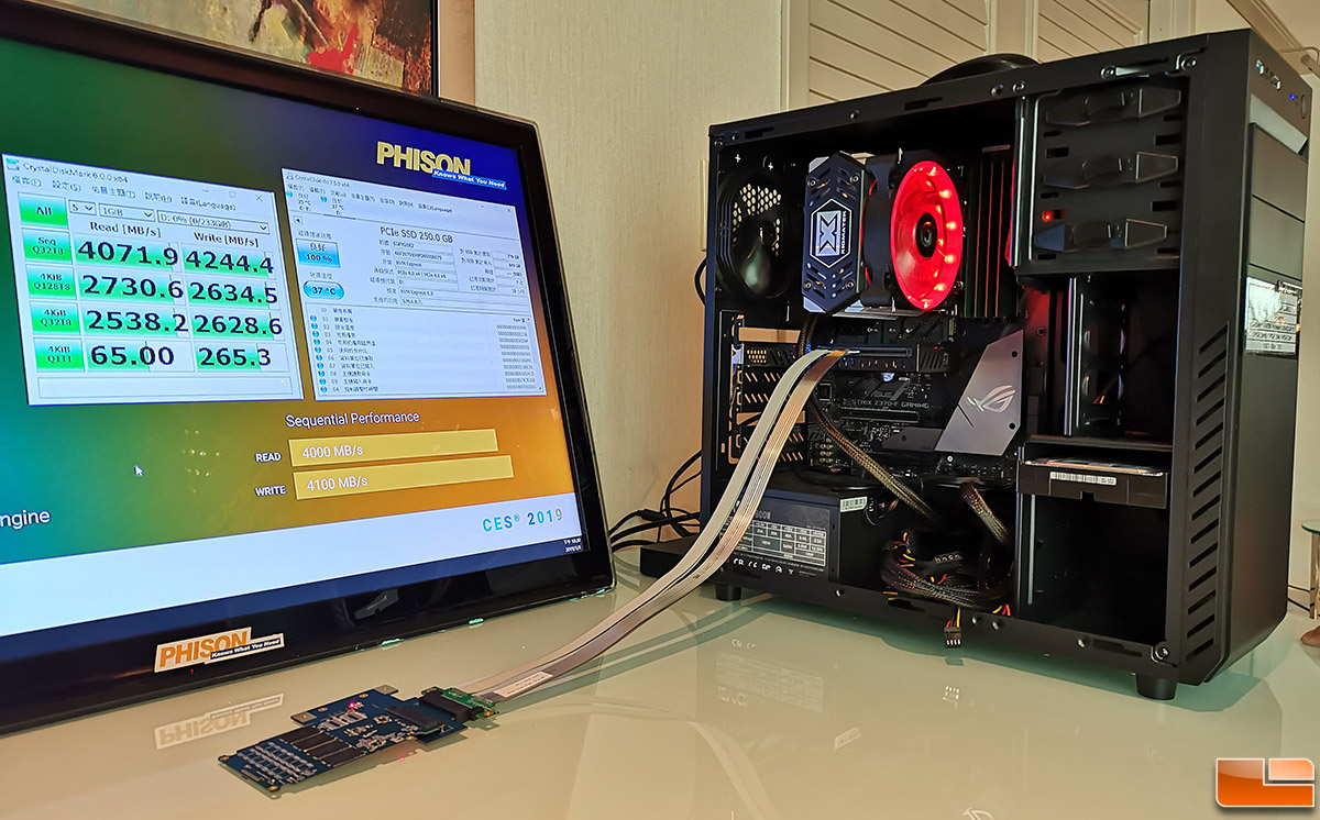
Phison PS5016-E16 PCIe Gen 4.0 x4 Demo at CES 2019 - Legit Reviews
 www.legitreviews.com
Last edited:
CrustyBritches
Gold Member
^^Now that's an actual Navi card from apisak.
I also see the reddit PS5 devkit specs leak, which is oddly specific. Either real or a very elaborate ruse.
Sapphire PR manager interview leak seemed real, too.
I also see the reddit PS5 devkit specs leak, which is oddly specific. Either real or a very elaborate ruse.
Sapphire PR manager interview leak seemed real, too.
grfunkulus
Banned
New leak with the price of the 3080 and 3070 putting slight better than 2070 card at $500 and slightly (but maybe more slightly) better than 2060 card at $400 can't bode well for the prices of these consoles...if accurate, those prices are nearly $200 more than the initial leaks...
SonGoku
Member
Retail pricing of discrete card is irrelevant to Console APUsNew leak with the price of the 3080 and 3070 putting slight better than 2070 card at $500 and slightly (but maybe more slightly) better than 2060 card at $400 can't bode well for the prices of these consoles...if accurate, those prices are nearly $200 more than the initial leaks...
What matters is die size and TDP.
Insane Metal
Gold Member
I don't think they will be APUs.
Imtjnotu
Member
Arcturus
Ovech-King
Gold Member
Interesting to think that 16GB DDR6 at 18 Gbps is more than the RTX 2080Ti at 11GB DDR6 14 Gbps ... at 1200$ US. Can't wait to see how the final product pans out. I expect 4K 60 fps on release
Insane Metal
Gold Member
Navi.Arcturus

TLZ
Banned
Hah!PlayStation 5 prototype spotted.
Note: Retail version will likely be smaller
How smaller? Hopefully fits a 3 story building
grfunkulus
Banned
Retail pricing of discrete card is irrelevant to Console APUs
What matters is die size and TDP.
Explain
SonGoku
Member
Price on the GPU consoles use depends on die size entirelyExplain
TDP determines what can be fitted into a console (180W max)
grfunkulus
Banned
Price on the GPU consoles use depends on die size entirely
TDP determines what can be fitted into a console (180W max)
Yeah, I know that. But on a basic, fundamental and economic level, the prices of gpus going up wouldn't drive the prices of other gpus with similarly technology up? Just sayin'
$500+ is looking more likely today than it was yesterday, can you really deny that?
CyberPanda
Banned
TLZ
Banned
Can someone translate this to layman please? Does it confirm we don't need super high TFs for better performance? So AMD don't need 13TF to perform as well as Nvidia's 9TF for example? Am I understanding this correctly?
Imtjnotu
Member
ArcturusNavi.
CyberPanda
Banned
Means that AMD cards are getting more efficient.Can someone translate this to layman please? Does it confirm we don't need super high TFs for better performance? So AMD don't need 13TF to perform as well as Nvidia's 9TF for example? Am I understanding this correctly?
TLZ
Banned
Can you explain the efficiency part, if you don't mind?Means that AMD cards are getting more efficient.
SonGoku
Member
Can you explain the efficiency part, if you don't mind?
Basically the more SE's you have in charge of CUs (or less CUs per SE) you can achieve better utilization of said CUs, which translates in less idle resources and the card coming closer to its peak performance in game scenariosAnother thing is the change from a single cluster of 4x16 SP's per CU (with a 64 Wave HW scheduler, and only ¼ of the sp's utilized per cycle) to 2x32 SIMDs per CUs. Thus, each CU gets better hardware scheduling (32-wave HW scheduler) to prevent under-utilization. The SIMD pipelines allow them to run simultaneously.
Think of SE's as teachers and CUs as children, the more teachers you have the more efficient the education alternatively if you have too many children per teacher some will fall under the radar and fool around in class (is idle)
Apart from that more SE's means: doubling of geometry & rasterization performance vs prior GCN designs
If this tweet is real, we are looking at potentially game changer stuff, the type of change you would expect from a post GCN design. It depends how good AMD design is to know how much closer they get to nvidia turing flops but one thing is for sure Navi flops>Vega flops
A 12TF Navi card could potentially enter RTX 2080/1080TI levels of performance.
Turing is more efficient than Pascal
1080TI: 11.34TF
RTX 2080: 10TF
Both cards have roughly same performance in old games, with RTX having advantage of new tech potentially giving it a big edge in future games (rt, async compute and vrs)
There could be other factors driving prices up, like poor initial yields, limited stock means its gonna sell out anywaysYeah, I know that. But on a basic, fundamental and economic level, the prices of gpus going up wouldn't drive the prices of other gpus with similarly technology up? Just sayin'
$500+ is looking more likely today than it was yesterday, can you really deny that?
Also remember semicustom is a different business, Sony and MS place orders in the millions.
I can see $500 happening with a small loss or cutting even.
Last edited:
SonGoku
Member
Here is a very detailed post i found there that helps understand the implications of this change:
This is the specific layout of a graphics card... a block diagram, you might say. All chips have a layout and design, with different parts organized to do different tasks. (Think of how you would organize a kitchen with 10 people doing different things to make a meal) While Zen is AMD's CPU design, Navi is their graphics card. This post has to do with AMD's Navi Graphics card (it's an upcoming card, expected to launch in Quarter 3 of this year).
For the last 6 or 7 years, AMD was really close to bankruptcy. They had decent graphics cards, but they'd made some critical mistakes in the CPU market, and Intel was hammering them to death. So AMD had this one old graphics card design called GCN that was really powerful when it came out (Early GCN was better known to the public has the Radeon HD 7970. It was faster than ANYTHING Nvidia had... kind of like the 2080Ti of its time).
But as the company ran out of money and had tons of debt, they had less and less money to make better designs. So, the Tahiti design (7970) was changed slightly when it became Hawaii and Tonga, AMD doubled the amount of triangles it could draw. (remember everything in graphics is made of triangles). But after that, Polaris and Vega were both stuck at 4 Triangles per clock.
Clock is each "cycle" -- 1 Hertz is 1 cycle per second. 1 Megahertz is 1 Million cycles per second. 1 Ghz is 1 Billion cycles per second. Because the AMD GPU's were stuck at 4 triangles per clock, and designs like Polaris were around 1.3Ghz, AMD was stuck with only 5.2 Billion Triangles per second of performance. Vega raised the number of clocks, but NOT the number of Triangles the card could draw. Meanwhile Nvidia cards manage 11 triangles per cycle... THIS is why the 1060 and 1080 pulled SO far ahead of Polaris and Vega.
This is one of the first AMD graphics designs that shows a lot of promise, because AMD has reorganized it and given us 8 geometry units, meaning it can now draw 8 triangles. This shows a lot of promise as it "widens" the pipeline - letting the cards do more triangle work per second.
Traditional GCN design is split into 4 blocks, where data is put into the pipe at the top, and travels through a shader and geometry engine, and then into a Compute Unit. Each Compute Unit has 64sp's, but they were split into 4 rows of 16.
The scheduler would put data in one of those pipes, but while that was happening, the other pipes would be waiting for their next instruction. So the big problems with GCN were:
Basically, this new design which leaked is a huge change to the AMD Graphics cards of the last few years, meaning that performance is expected to be very good.
I hope this explanation helps you get a grasp of what's going on. I did simplify a few things, and I may not have explained everything well. Please ask questions an I'll try to answer them.
welcome to /r/hardware. You'll learn a LOT here. (I know I still do)
For the last 6 or 7 years, AMD was really close to bankruptcy. They had decent graphics cards, but they'd made some critical mistakes in the CPU market, and Intel was hammering them to death. So AMD had this one old graphics card design called GCN that was really powerful when it came out (Early GCN was better known to the public has the Radeon HD 7970. It was faster than ANYTHING Nvidia had... kind of like the 2080Ti of its time).
But as the company ran out of money and had tons of debt, they had less and less money to make better designs. So, the Tahiti design (7970) was changed slightly when it became Hawaii and Tonga, AMD doubled the amount of triangles it could draw. (remember everything in graphics is made of triangles). But after that, Polaris and Vega were both stuck at 4 Triangles per clock.
Clock is each "cycle" -- 1 Hertz is 1 cycle per second. 1 Megahertz is 1 Million cycles per second. 1 Ghz is 1 Billion cycles per second. Because the AMD GPU's were stuck at 4 triangles per clock, and designs like Polaris were around 1.3Ghz, AMD was stuck with only 5.2 Billion Triangles per second of performance. Vega raised the number of clocks, but NOT the number of Triangles the card could draw. Meanwhile Nvidia cards manage 11 triangles per cycle... THIS is why the 1060 and 1080 pulled SO far ahead of Polaris and Vega.
This is one of the first AMD graphics designs that shows a lot of promise, because AMD has reorganized it and given us 8 geometry units, meaning it can now draw 8 triangles. This shows a lot of promise as it "widens" the pipeline - letting the cards do more triangle work per second.
Traditional GCN design is split into 4 blocks, where data is put into the pipe at the top, and travels through a shader and geometry engine, and then into a Compute Unit. Each Compute Unit has 64sp's, but they were split into 4 rows of 16.
The scheduler would put data in one of those pipes, but while that was happening, the other pipes would be waiting for their next instruction. So the big problems with GCN were:
- it was data starved. There was never enough data to keep all the SP's running at once (only 16 of 64 were running at any given time), unless the coders were very clever and specifically wrote their game / code / application to use all the pipes.
- Because the frontend of Geometry and shaders was only 4-wide, there was a bottleneck. The card could not do shading or draw triangles quickly enough to keep everything fed.
Basically, this new design which leaked is a huge change to the AMD Graphics cards of the last few years, meaning that performance is expected to be very good.
I hope this explanation helps you get a grasp of what's going on. I did simplify a few things, and I may not have explained everything well. Please ask questions an I'll try to answer them.
welcome to /r/hardware. You'll learn a LOT here. (I know I still do)
Tarkus98
Member
Damn! Wow. If true wouldn’t this place Microsoft’s design engineers into the realm of time travelers? I mean how could they otherwise have possibly known about these theoretical Navi hurdles before even AMD? Then to wisely choose to brute force Vega into submission making it more powerful then AMD could even have hoped for. Well, shit this is incredible if true. I think I will believe this one! I also bet they are actually the ones that nabbed that CELL2 secret sauce too. Yep. It’s all becoming too clear now.I hate feeding into this garbage but, I'll bite.

Third party developer here with contacts at AMD from the old days. Just got our - Pastebin.com
Pastebin.com is the number one paste tool since 2002. Pastebin is a website where you can store text online for a set period of time.pastebin.com
Shangounchained
Banned
Point is it won't make any big difference besides popin you'd see the same assets on a single frame, we need larger memory sizes for next gen so we can have more assets on a frame, memory size is always an issue in consoles I swear to you if the ps5 has 8 or 12 GB then there is no point making itI mean, that's the point.
DemonCleaner
Member
exciting times ahead of us
if that is indeed real
if that is indeed real
DemonCleaner
Member
in the meantime i've done some rigorous research (asking dumb questions)
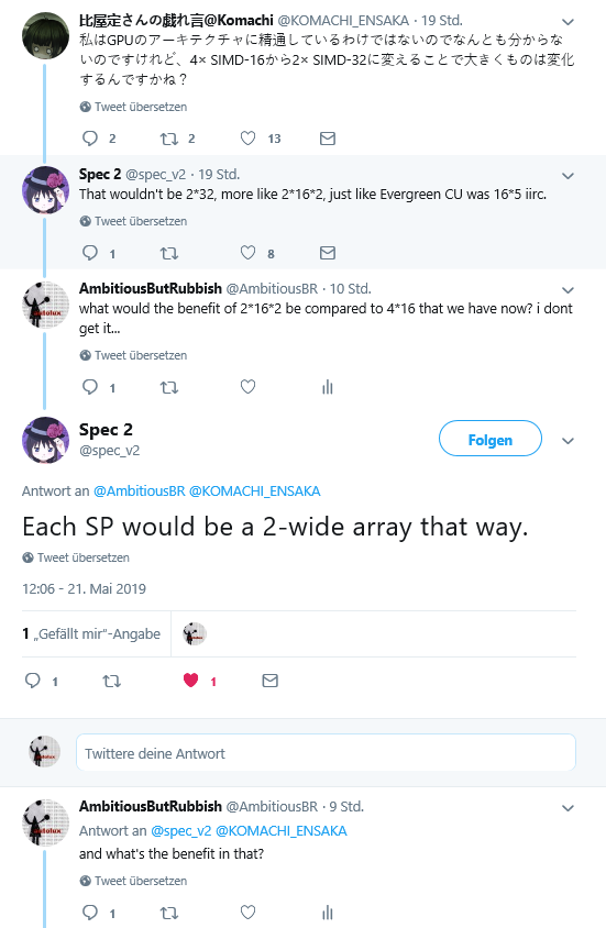
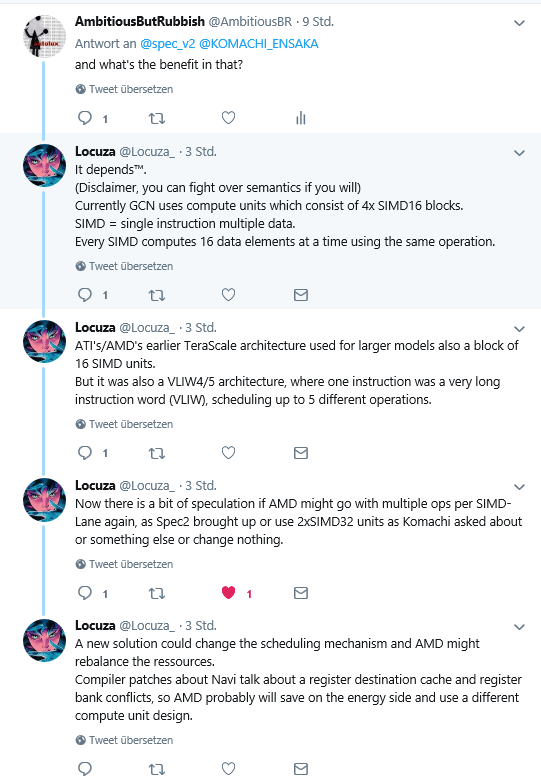
so it looks like the benefit of the new SIMD design is that you can do two different operations concurrently per SIMD
so it looks like the benefit of the new SIMD design is that you can do two different operations concurrently per SIMD
Imtjnotu
Member
So at the same clock (1.3)we can get over 10 billion triangles. If that random ass 1.8ghz is true were looking at 14 billionHere is a very detailed post i found there that helps understand the implications of this change:
This is the specific layout of a graphics card... a block diagram, you might say. All chips have a layout and design, with different parts organized to do different tasks. (Think of how you would organize a kitchen with 10 people doing different things to make a meal) While Zen is AMD's CPU design, Navi is their graphics card. This post has to do with AMD's Navi Graphics card (it's an upcoming card, expected to launch in Quarter 3 of this year).
For the last 6 or 7 years, AMD was really close to bankruptcy. They had decent graphics cards, but they'd made some critical mistakes in the CPU market, and Intel was hammering them to death. So AMD had this one old graphics card design called GCN that was really powerful when it came out (Early GCN was better known to the public has the Radeon HD 7970. It was faster than ANYTHING Nvidia had... kind of like the 2080Ti of its time).
But as the company ran out of money and had tons of debt, they had less and less money to make better designs. So, the Tahiti design (7970) was changed slightly when it became Hawaii and Tonga, AMD doubled the amount of triangles it could draw. (remember everything in graphics is made of triangles). But after that, Polaris and Vega were both stuck at 4 Triangles per clock.
Clock is each "cycle" -- 1 Hertz is 1 cycle per second. 1 Megahertz is 1 Million cycles per second. 1 Ghz is 1 Billion cycles per second. Because the AMD GPU's were stuck at 4 triangles per clock, and designs like Polaris were around 1.3Ghz, AMD was stuck with only 5.2 Billion Triangles per second of performance. Vega raised the number of clocks, but NOT the number of Triangles the card could draw. Meanwhile Nvidia cards manage 11 triangles per cycle... THIS is why the 1060 and 1080 pulled SO far ahead of Polaris and Vega.
This is one of the first AMD graphics designs that shows a lot of promise, because AMD has reorganized it and given us 8 geometry units, meaning it can now draw 8 triangles. This shows a lot of promise as it "widens" the pipeline - letting the cards do more triangle work per second.
Traditional GCN design is split into 4 blocks, where data is put into the pipe at the top, and travels through a shader and geometry engine, and then into a Compute Unit. Each Compute Unit has 64sp's, but they were split into 4 rows of 16.
The scheduler would put data in one of those pipes, but while that was happening, the other pipes would be waiting for their next instruction. So the big problems with GCN were:
This new design WIDENS the front, and then makes 2 rows of 32 that can run simultaneously, with Multiple datasets at once, all following the same instructions. So this new design can draw triangles faster, do more shading, and make more frames quickly, leading to better performance.
- it was data starved. There was never enough data to keep all the SP's running at once (only 16 of 64 were running at any given time), unless the coders were very clever and specifically wrote their game / code / application to use all the pipes.
- Because the frontend of Geometry and shaders was only 4-wide, there was a bottleneck. The card could not do shading or draw triangles quickly enough to keep everything fed.
Basically, this new design which leaked is a huge change to the AMD Graphics cards of the last few years, meaning that performance is expected to be very good.
I hope this explanation helps you get a grasp of what's going on. I did simplify a few things, and I may not have explained everything well. Please ask questions an I'll try to answer them.
welcome to /r/hardware. You'll learn a LOT here. (I know I still do)
DemonCleaner
Member
well that basically just condenses what we said the past few pages.
Apart from that more SE's means: doubling of geometry & rasterization performance vs prior GCN designs
i don't think the doubleling of rasterization perf is really important hence GCN was not really limited by that. it just comes as a result of doubling the SEs. shouldn't have any significant real world Impact. doubling of geo processing on the other hand... thats the huge part.
Turing is more efficient than Pascal
1080TI: 11.34TF
RTX 2080: 10TF
Both cards have roughly same performance in old games, with RTX having advantage of new tech potentially giving it a big edge in future games (rt, async compute and vrs)
turing is more flop efficient compared to pascal because they use concurrent integer processing which isn't taken into acount in the FLOP number. it comes at a rather big price for die area real estate. one has to keep that in mind.
I can see $500 happening with a small loss or cutting even.
if the APU was ~320mm² they should be able to sell at $500 with a small profit
Last edited:
CyberPanda
Banned
DemonCleaner
Member
DemonCleaner . Please use the regular text colour for the forum. I have the dark theme on currently, and your text is grey and I can't even read it. Thanks.
didn't change that. i think my browser is screwing with me. edited the last post. does it work now?
Last edited:
CyberPanda
Banned
Yep, it's fixed. Thank you.didn't chage that. i think my browser is screwing with me. edit the last post. does it work now?
Ar¢tos
Member
Sticky White Stuff!!On a more serious note, new leak from @SUM_HAPISAK from worker inside Foxconn manufacturing facility...

Demon's Souls Remake confirmed!
xool
Member
Yeah, I know that. But on a basic, fundamental and economic level, the prices of gpus going up wouldn't drive the prices of other gpus with similarly technology up? Just sayin'
It would do if there was direct competition - but there isn't because a. Nvidia doesn't even try to compete in console space because profit margins are too low (allegedly)[wouldn't increase prices anyway], and b. Consoles are a different business area/model from PC space.
Also AMD is a company that made [7% profit margin] $450m profit on revenue of $6500m (2018) .. Nvidia made [34% profit margin] $4100m on revenue $12000m and that was AMD's best results in 7 years (because Zen ?) .
AMD is on the edge, and takes much reduced margins.
;tldr AMD is working to keep the lights on
Last edited:
bitbydeath
Gold Member
Just watching Love, Death and Robots - The Secret War. I wonder if this is the sorts of graphics we will be getting next-gen.

Last edited:
nowhat
Member
There are few episodes in there that made me think "now why do we have actors again"? Uncanny valley and all that, but CGI is reaching a threshold where it manages to escape it.Just watching Love, Death and Robots - The Secret War. I wonder if this is the sorts of graphics we will be getting next-gen.
pawel86ck
Banned
Again, PC fanboys have said there will be no arch changes in Navi, because that's still GCN and 12.9TF in PS5 will only translate into GTX 1070 performance territoryHere is a very detailed post i found there that helps understand the implications of this change:
This is the specific layout of a graphics card... a block diagram, you might say. All chips have a layout and design, with different parts organized to do different tasks. (Think of how you would organize a kitchen with 10 people doing different things to make a meal) While Zen is AMD's CPU design, Navi is their graphics card. This post has to do with AMD's Navi Graphics card (it's an upcoming card, expected to launch in Quarter 3 of this year).
For the last 6 or 7 years, AMD was really close to bankruptcy. They had decent graphics cards, but they'd made some critical mistakes in the CPU market, and Intel was hammering them to death. So AMD had this one old graphics card design called GCN that was really powerful when it came out (Early GCN was better known to the public has the Radeon HD 7970. It was faster than ANYTHING Nvidia had... kind of like the 2080Ti of its time).
But as the company ran out of money and had tons of debt, they had less and less money to make better designs. So, the Tahiti design (7970) was changed slightly when it became Hawaii and Tonga, AMD doubled the amount of triangles it could draw. (remember everything in graphics is made of triangles). But after that, Polaris and Vega were both stuck at 4 Triangles per clock.
Clock is each "cycle" -- 1 Hertz is 1 cycle per second. 1 Megahertz is 1 Million cycles per second. 1 Ghz is 1 Billion cycles per second. Because the AMD GPU's were stuck at 4 triangles per clock, and designs like Polaris were around 1.3Ghz, AMD was stuck with only 5.2 Billion Triangles per second of performance. Vega raised the number of clocks, but NOT the number of Triangles the card could draw. Meanwhile Nvidia cards manage 11 triangles per cycle... THIS is why the 1060 and 1080 pulled SO far ahead of Polaris and Vega.
This is one of the first AMD graphics designs that shows a lot of promise, because AMD has reorganized it and given us 8 geometry units, meaning it can now draw 8 triangles. This shows a lot of promise as it "widens" the pipeline - letting the cards do more triangle work per second.
Traditional GCN design is split into 4 blocks, where data is put into the pipe at the top, and travels through a shader and geometry engine, and then into a Compute Unit. Each Compute Unit has 64sp's, but they were split into 4 rows of 16.
The scheduler would put data in one of those pipes, but while that was happening, the other pipes would be waiting for their next instruction. So the big problems with GCN were:
This new design WIDENS the front, and then makes 2 rows of 32 that can run simultaneously, with Multiple datasets at once, all following the same instructions. So this new design can draw triangles faster, do more shading, and make more frames quickly, leading to better performance.
- it was data starved. There was never enough data to keep all the SP's running at once (only 16 of 64 were running at any given time), unless the coders were very clever and specifically wrote their game / code / application to use all the pipes.
- Because the frontend of Geometry and shaders was only 4-wide, there was a bottleneck. The card could not do shading or draw triangles quickly enough to keep everything fed.
Basically, this new design which leaked is a huge change to the AMD Graphics cards of the last few years, meaning that performance is expected to be very good.
I hope this explanation helps you get a grasp of what's going on. I did simplify a few things, and I may not have explained everything well. Please ask questions an I'll try to answer them.
welcome to /r/hardware. You'll learn a LOT here. (I know I still do)
 . And dont even dream about 24 GB RAM and HW RT, because that's cheap console so people will be lucky to see just 16 GB in PS5, and because software RT in MineCraft can be run at 30fps 720p on GTX 1070, so PS5 will not need HW RT solution for 1440-4K resolutions
I dont even want to quote these PC fanboys here, but they should have some dignity and stop trying so hard to downplay nextgens from both SONY and MS.
Jokes aside, new generatrion will rise HW requirements on PC to the roof, and especially when it comes to VRAM usage. If games made with PS4/XBO in mind require already around 6GB vram when ported to PC, then imagine what will happen when PS5 multiplatform games starts showing up. If PS5 will use around 24 GB and lets say 20 GB will be available to games, then PS5 multiplatform games on PC can use even over 10 GB VRAM. But on PC people can of course always lower texture settings even way below PS5 settings, so I'm guessing GTX 1070 users should be fine for the next 8 years

Last edited:
bitbydeath
Gold Member
There are few episodes in there that made me think "now why do we have actors again"? Uncanny valley and all that, but CGI is reaching a threshold where it manages to escape it.
Yeah, this episode in particular looked incredibly real at times with the surroundings but often the people would break the immersion. Graphics will obviously take a jump and I think the graphics on that episode is not out of reach.
SonGoku
Member
Launch PS4 was 348mm2 and xbone over 350mm2if the APU was ~320mm² they should be able to sell at $500 with a small profit
BTW he is saying 8 Shader Engine with 5 CUs each... that means 40CUs total (Polaris number os units).
They changed from SIMD-16 to SIMD-32... that means the limit of 16CUs per SE is now 8 CUs per SE.
Still the same 64CUs max.
Im confused, is the limit 40CUs or 64CUs?
Last edited:
TeamGhobad
Banned
Launch PS4 was 348mm2 and xbone over 350mm2
Im confused, is the limit 40CUs or 64CUs?
and if there are 5 CU's for every SE, how do we get to 64? last SE has 4 CU's???
ethomaz
Banned
64CUs... 8SE with 8CU each in that new way... 4SE with 16CU each in the old way.Im confused, is the limit 40CUs or 64CUs?
But Navi 10 is a mid/mainstream 40CU chip... 8SE with 5CU each.
The 64CU Navi only next year with Navi 20.
PS. I posted the max limit of the Arch more because the next-gen console can have a Navi up to 64CUs (8SE with 8CU each) while AMD will only launch the 40CU Navi this year.
Last edited:
xool
Member
and if there are 5 CU's for every SE, how do we get to 64? last SE has 4 CU's???
Im confused, is the limit 40CUs or 64CUs?
I think he/she was just quoting for a specific part - so it was a 40CU chip (5 not the new limit)
Last edited:
TeamGhobad
Banned
I think he/she was just quoting for a specific part - so it was a 40CU chip (5 not the new limit)
so 5 CU's is not the limit for every SE....interesting but how sure are we about this? the leak said 5CUs for every SE no mention of more.
Last edited:
ethomaz
Banned
Yeap 8CU per SE is the new limit.I think he/she was just quoting for a specific part - so it was a 40CU chip (5 not the new limit)
But Navi chip AMD is launching this year will have only 5CU per SE... Next year they will launch the sucessor of Vega 7nm with 64CU.
The arch is not changing... they are changing how the scheduler/waves works internally.so 5 CU's is not the limit for every SE....interesting but how sure are we about this?
Last edited:
xool
Member
I can't find the originalso 5 CU's is not the limit for every SE....interesting but how sure are we about this? the leak said 5CUs for every SE no mention of more.
Maybe more than 5 and it's Navi 20 .. (also 5 is an odd number [literally /jk] to cap at .. would be really strange)
Last edited:
Ellery
Member
The Navi improvements are actually extremely interesting for us because it means that even if the PS5 has a somewhat "low" number of TFLOPs, which is mostly dictated by our skewed perception, it could still be a huge improvement. An 8TF Navi PS5 could be better than lets say a 10TF Vega PS5.
Really excited about this
Really excited about this
TeamGhobad
Banned
Lets speculate for a moment. lets pretend PS5 has navi 8 SE * 8 CUs and Xbox2 has vega 4 SE * 16 CUs, same clocks obviously. how much difference will there be in graphics/power? anything noticeable?
Lets speculate for a moment. lets pretend PS5 has navi 8 SE x 8 CUs and Xbox2 has vega 4 SE * 16 CUs. how much difference will there be in graphics?
yes but educating the public about this is going to be very hard. marketing will have its hands full.
Lets speculate for a moment. lets pretend PS5 has navi 8 SE x 8 CUs and Xbox2 has vega 4 SE * 16 CUs. how much difference will there be in graphics?
The Navi improvements are actually extremely interesting for us because it means that even if the PS5 has a somewhat "low" number of TFLOPs, which is mostly dictated by our skewed perception, it could still be a huge improvement. An 8TF Navi PS5 could be better than lets say a 10TF Vega PS5.
Really excited about this
yes but educating the public about this is going to be very hard. marketing will have its hands full.
Last edited:
ethomaz
Banned
In graphical processing power? None... both chip will have the same peak capabilities.Lets speculate for a moment. lets pretend PS5 has navi 8 SE * 8 CUs and Xbox2 has vega 4 SE * 16 CUs, same clocks obviously. how much difference will there be in graphics/power? anything noticeable?
The scheduler is changing to be more balanced and efficient but it continue having the same processing power than before.
But with 8SE you can double the number of ROPs that helps in the Render Output.
BTW developer can code to take max performance for each way the difference is that the old way you need to take a big more care with the waves of data processing than the new way.
Last edited:
FranXico
Member
If they have games to show the increased power, it's doable.yes but educating the public about this is going to be very hard. marketing will have its hands full.
SonGoku
Member
Indeed or a 12TF Navi could be comparable to a 1080Ti/RTX2080The Navi improvements are actually extremely interesting for us because it means that even if the PS5 has a somewhat "low" number of TFLOPs, which is mostly dictated by our skewed perception, it could still be a huge improvement. An 8TF Navi PS5 could be better than lets say a 10TF Vega PS5.
Really excited about this
Shouldn't be as long as PC benchmarks show how it performs compared to previous AMD cards and Nvidiayes but educating the public about this is going to be very hard. marketing will have its hands full.
Last edited:
ethomaz
Banned
Let's do a better explanation (I guess).
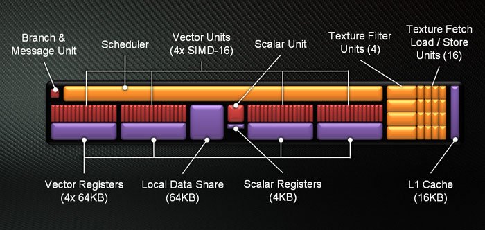
That is the actual CU in GCN up to version 5.1 (or 1.5.1):
* maybe the cache changed between versions but the numbers of units never changed until now.
What that means?
That means a CU in GCN has 4x SIMD-16 lanes per CU, or in easy terms, GCN has 4 goups of 16SPs in each CU.
To use these SPs you need to schedule waves of 16 processing instructions of the same type (the data can be different but the instruction needs to be the same).
That way the minimum you run in a CU is 16SPs per time and the max 64SPs per time but they needs to be in waves of 16SPs... trying to make it easy you need 64 same processing instructions send in 4 waves to fullfill a CU... if your code was not optimized for that then it will use 1, 2 or 3 waves instead of 4.
That generate inefficiency because you have a CU with 64SPs but most of time it is using 16, 32 or 48SPs only.
You need to optimize the code to take advantage and runs most of time with 64SPs at full work in a CU.
In simple terms, actual CGN schedule tasks in waves of 16SPs in a CU.
The worst case scenario a CU will use only 16SPs... best case scenario the CU will use 64SPs... there is the middle always in waves of 16 so 32 and 48 SPs being used.
What changes in the GCN 6.0 (or 1.6.0)?
The SIMD-16 wave is changed to SIMD-32 wave... that way you need 32SPs of the same type instruction being schedule in waves for a CU... the CU will always run with 32CUs or at max 64SPs... there is no middle and the wave is the minimum 32SPs.
That means more efficiency?
In terms... the change make the minimum your CU can be using is 32SPs instead of 16SPs in the past that indeed means the CU will be always at least being used at half-power while before it could be used at 1/4 of it power... that means less SPs per SP in idle (not doing anything).
But here is maybe the big issue... it is easier to group SPs in waves of 16 instead 32.
If you can't group 16 (old) or 32 (new) same type of processing instruction to make a wave then you will even to use only one SP send a wave of 16/32 that makes the power consumption increase in the new way because you will have always running a wave with 32SPs even when you need to use only one SP... before you needed only a wave of 16SPs running to use one SP.
So if the Scheduler is not smart (the magic needs to be here) to group waves of 32 instructions the perf/watt will decrease, the efficiency will decrease because it is easier to group waves of 16 than 32.
So you have two sides:
1) It become more efficient because it will always be using at least half of 64SPs in a CU.
2) It become less efficient if the Scheduler can't group waves of 32 instructions.
The biggest change that nobody is talking is how the Scheduler will do that magic to make the new GCN design more efficient.
Of course there is side advantages too like the increase in Render Output units.
You are still limited to 64CUs but the limit for others units increased:
4 to 8 SEs
64 to 128 ROPs
Last edited:
Ellery
Member
Im confused, is the limit 40CUs or 64CUs
Indeed or a 12TF Navi could be comparable to a 1080Ti/RTX2080
Shouldn't be as long as PC benchmarks show how it performs compared to previous AMD cards and Nvidia
yeah currently, and at CES actually, there was a lot of talk about a 9.2 TFLOPs PS5 which would make a lot of sense being on a smaller Navi chip.
IF the rumors are true abut the SE's then we won't get a 12TF Navi this year, because that card would be better than the Vega VII and that card remains their flagship until 2020.
IF the rumors aren't true then a 12TF Navi would basically just be like a 12TF Vega 64 or so.
- Status
- Not open for further replies.