-
Hey, guest user. Hope you're enjoying NeoGAF! Have you considered registering for an account? Come join us and add your take to the daily discourse.
You are using an out of date browser. It may not display this or other websites correctly.
You should upgrade or use an alternative browser.
You should upgrade or use an alternative browser.
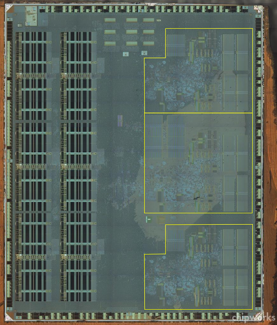
Wii U CPU |Espresso| Die Photo - Courtesy of Chipworks
- Thread starter Fourth Storm
- Start date
bgassassin
Member
I suck at drawing and can't even consistently draw straight lines with a tool, but I made a couple of approximations of the cores.

Yeah, the GPU thread brought me back and since they said the CPU was coming I waited.
Ok. Glad you found that much.
I didn't know the formula, but I did feel it was supposed to be smaller than LiB's calculation. I've seen it where just transitioning to the next node has reduced size by like 30%.
you're back o:
Yeah, the GPU thread brought me back and since they said the CPU was coming I waited.
Taking Broadway aside... Sadly yes; I left the sources for them linked to the images though; but for Flipper and PPC 750 the images are really that sized.
Ok. Glad you found that much.
Wouldn't the shrink from 90nm to 45nm be a quarter the area (45/90)² for a die of 4.725mm² ?
I didn't know the formula, but I did feel it was supposed to be smaller than LiB's calculation. I've seen it where just transitioning to the next node has reduced size by like 30%.
lostinblue
Banned
Could be, I thought about it before writing. But... I don't think so.Wouldn't the shrink from 90nm to 45nm be a quarter the area (45/90)² for a die of 4.725mm² ?
My reasoning was that Broadway (90 nm) is also manufactured at half of Gekko's 180 nm process and it sits at roughly half the die area instead of a fourth. But... it's also less than half by 2 mm² or so and seems to have added things (and the size proportion of the cache banks changed in there)
I was probably oversimplifying it, but if anyone knows how to go about it please do. All in all though, it feels fishy, if each of those dies are the equivalent of a Gekko/Broadway (or even just the middle one), feature 4 times the cache and have that left sided block thing going on, I reckon it's kinda small.
TheLastCandle
Member
I see, said the blind man.
bgassassin
Member
I think you can see that they're three of the same a bit better if you separate out the cache.

I believe those are the SRAM tags as wsippel said, that said I like yours better.
Mentallyerect
Neo Member
Lurker here, love what you guys have been doing with the GPU thread and now this (even though must of this is over my head) Quick question though. Once those of you who are breaking these images down get the best hypothesis on what both the GPU and CPU are, will you create another thread detailing both and how the possibly coexist and work off each other to their benefit?

blu
Wants the largest console games publisher to avoid Nintendo's platforms.
I believe those are the SRAM tags as wsippel said, that said I like yours better.
Or not. The area calculation does not come right for those to account for the L2.
lostinblue
Banned
Oh, never thought about them as L2 tags. Might be; never mind what I said regarding expected die size; I was counting that left block as something other than cache.I believe those are the SRAM tags as wsippel said, that said I like yours better.
lwilliams3
Member
Oh yeah, edited.
Oh wait... hmm. I first thought the black block on the left was I/O and what I marked in magenta was the L2, but I resized the GPU photo to the same scale and they seemed too small.
Are the CPU and GPU on the same process?
The GPU is likely 40nm. The CPU is confirmed to be 45nm.
blu
Wants the largest console games publisher to avoid Nintendo's platforms.
Nope - 45 vs 40 (and different fabs - IBM vs TSMC).Oh wait... hmm. I first thought the black block on the left was I/O and what I marked in magenta was the L2, but I resized the GPU photo to the same scale and they seemed too small.
Are the CPU and GPU on the same process?
I'm currently of the opinion the black area on the left are the eDRAM macros, the areas you marked in magenta are indeed tags (SRAM), and the logic in between the L2 and the cores is SMP interconnect fabric. The 9 SRAM pools in the top-middle are some sizeable of IO buffers - perhaps for the DMA engines.
bgassassin
Member
Those are the L2 eDRAM macros, IMHO.
Or not. The area calculation does not come right for those to account for the L2.
Those being the L2 tags do make the most sense, because the black blocks seem the be the L2 cache. Like I mentioned I calculated each of those blocks to be 256KB.
I see you're saying they are the tags now, haha.
Oh yeah, edited.
Oh wait... hmm. I first thought black block on the left was I/O and what I marked in magenta was the L2, but I resized the GPU photo to the same scale and they seemed too small.
Are the CPU and GPU on the same process?
CPU is 45nm. But yeah the L2 cache has to be the black blocks.
Soooo..........I'm lost here. Is this and upgraded/updated Broadway that was used in the Wii or is it something completely different?
Probably depends on perspective. When the poster Espresso talked about it on B3D he focused on the the few features given that came from Gekko/Broadway. However that line could not be clocked at Espresso's current clock and I don't believe they could support the amount of cache that the main core does as well. IMO I would say it definitely is not a straight up Gekko/Broadway. But there were things done for BC purposes.
lostinblue
Banned
It's most likely still PPC 750 based though otherwise they couldn't keep code compatibility locked down.IMO I would say it definitely is not a straight up Gekko/Broadway. But there were things done for BC purposes.
I'm way more curious if they added things to it; more SIMD instructions (like VMX128) or enhanced integer. But I'm not counting on it.
lostinblue
Banned
With a core shrink this agressive, it most likely could. I mean you had PowerPC 750GX pulling 1.1 GHz @ 130 nm's.However that line could not be clocked at Espresso's current clock
1.24 GHz is a small step considering it's 45 nm's now, and probably down to MHz/Watt consumption sweet spot and cooling concerns.
Espresso said this back in June:
"It isn't power7. it isn't SPU or cell. it isn't a 4xx. It is the same core as Wii, with 3 of them and larger L2's, clocked a little bit faster."
Going to side with him considering he knew the code name before any of us.
this is something many people know from wii age... it cant be wii cores.. because the tech of wii core, was not able to come in a multi core chip... and it couldnt come in higher clocks.. its something different
Quoting myself from a few emails yesterday:
I'll have some more to add when I get home from work later on today.
Thraktor said:This is a lot more straight-forward. The left is (obviously) the L2 eDRAM cache, in six 512KB cells. They seem to be laid out in a slightly different way than on either the A2 or Power7, but there's probably a relatively mundane reason behind that. We have three identical cores, the only difference being the centre one has four times the amount of SRAM for L2 tags (the four blocks near the middle), indicating it's the one with the 2MB of L2.
To the right of each core there's the L1 instruction and data caches (32KB each, I assume). I'm guessing the "strips" of SRAM to the upper left of the L1 caches are the L1 cache tags (again, one each for instruction and data).
The big "gap" in the middle is a mix of L2 cache logic and SMP interconnect (have a look at the Power7 and you'll see a similar proportion of such logic in the centre of the chip).
I'm going to guess that the long green things in the middle of each core are the registers (one for general purpose registers and one for floating point registers).
I will say that it's pretty difficult to say whether there have been any notable changes to the cores over Broadway. While we do have a Broadway shot from Marcan, you'd really need one taken using the same process as this by Chipworks to make a proper comparison. I've had a quick look over Power7 and BG/Q die shots to see if I could notice anything that might give us clues, but nothing popped out at me. I'll have a more thorough look later.
Thraktor said:does anyone else find it a bit odd that the L1 is on the opposite end of the cores to the L2?
Thraktor said:Also, as a point of reference people might want to read this description of the 750 architecture:
http://arstechnica.com/features/2004/10/ppc-2/
and have a look at this labelled 750 die photo:
http://gecko54000.free.fr/documentations/images/dies/thm_IBM_PPC_750_anatomy.jpg
to give you an idea of what components are inside the cores.
The small in-core pieces of SRAM are mainly going to be the instruction queue, reservation stations, completion queue, branch target instruction cache and branch history table.
I'll have some more to add when I get home from work later on today.
Naked Snake
Member
Only three Wii cores? Sounds weaksauce
I guess Dolphin emulation of Wii U is eminent?
I guess Dolphin emulation of Wii U is eminent?
bgassassin
Member
It's most likely still PPC 750 based though otherwise they couldn't keep code compatibility locked down.
I'm way more curious if they added things to it; more SIMD instructions (like VMX128) or enhanced integer. But I'm not counting on it.
Based on it I can see.
With a core shrink this agressive, it most likely could. I mean you had PowerPC 750GX pulling 1.1 GHz @ 130 nm's.
1.24 GHz is a small step considering it's 45 nm's now, and probably down to MHz/Watt consumption sweet spot and cooling concerns.
Orionas mentioned the VX, which I didn't know about, and that did achieve higher speeds.
Espresso said this back in June:
"It isn't power7. it isn't SPU or cell. it isn't a 4xx. It is the same core as Wii, with 3 of them and larger L2's, clocked a little bit faster."
Going to side with him considering he knew the code name before any of us.
You only took a portion of that post. Apparently his evidence was based on the limited features given in the docs. Looks at the features he gave in that post and then look at what was leaked by VGLeaks.
http://www.vgleaks.com/world-premiere-wii-u-specs/
I think you can see that they're three of the same a bit better if you separate out the cache tags.
The areas above the L1 that you have as gaps between the cores are actually part of the core logic, as far as I can tell. My current theory is that this is where the LSU resides in each core.
Seems like there's a lot of "dead space" between the cores and the eDRAM. Any thoughts on to why? For thermal issues, perhaps?
Some of it's cache logic, the rest is for communication between the cores.
lostinblue
Banned
Did it? I didn't know about it either but sounds like an urban myth and even if it wasn't it never reached production.Orionas mentioned the VX, which I didn't know about, and that did achieve higher speeds.
PowerPC G3+Altivec and "probably" 1.25 GHz and up? It's not listed or documented by IBM to this day too. I'm sure it could be done but I'm not so sure it was done; even posts from the time in that thread question it's existence.
VX seems like old rumors/conjecture that never came to fruition, PPC750 CL was released as late as 2006; VX never did. I agree it could be a best case scenario for this chip, but I doubt it.
Only if you're emulating Wii U emulating a Wii game.Only three Wii cores? Sounds weaksauce
I guess Dolphin emulation of Wii U is eminent?
bgassassin
Member
Did it? I didn't know about it either but sounds like an urban myth and even if it wasn't it never reached production.
PowerPC G3+Altivec and "probably" 1.25 GHz and up? It's not listed or documented by IBM to this day too. I'm sure it could be done but I'm not so sure it was done.
VX seems like 2003 rumors/conjecture that never came to fruition, PPC750 CL was released as late as 2006; but no VX.
Yeah. As I searched further it seemed to be on paper only.
Did it? I didn't know about it either but sounds like an urban myth and even if it wasn't it never reached production.
PowerPC G3+Altivec and "probably" 1.25 GHz and up? It's not listed or documented by IBM to this day too. I'm sure it could be done but I'm not so sure it was done; even posts from the time in that thread question it's existence.
VX seems like old rumors/conjecture that never came to fruition, PPC750 CL was released as late as 2006; VX never did. I agree it could be a best case scenario for this chip, but I doubt it.Only if you're emulating Wii U emulating a Wii game.
I transfered the opinion of a wii U member.. its not mine, but he also said that the cpu was ready for Apple, but apple abandoned this and alianced with Intel and created the "i core"
so here is the message I hope this guy helps, he is specwise, I am sure he is reading also here
'''These look to be 3 (custom) ppc750 fx's, and the fat boy in the middle is a little wierd, its the same size as the fx's, but it appears to have a few extra logic components.... And twice the cache of the 750Gx (but it if it was a gx, it would be noticably larger than its buddies above and below... which its not.)
These are all code compatable with every processor in the 750 family, including 750Cx (Gekko) 750cle (broadway) (and any and all g3 computers/ibooks/laptops)
A little info about the difference between 750fx and cle.
Fx has about twice the transistor count of cle, and smokes in instructions per clock and performance per watt.... And it has never, EVER been fabricated this small or clocked this high.... or made multicore.
It would be epically hilarious if this ended up being a derivitive of the mythical 750vx. IBM was planning a ppc750 to replace the disasterous 64bit ppc 970 (g4's/g5's, what would eventually be the basis of both xenon and cell)
It was the ppc750Vx, and at 2Ghz, a vertex engine and just 1 core, it could handidly outperform tricore g4's clocked considerably higher... Which would have placed it paralell to the g5 as a replacement to the g4.
Vx never saw the light of day because apple ended their partnership with ibm over the piss poor performance of the 970, and forged a an alliance with intel, creating the icore. ''''''
")
Why take a picture of something that's old and dying
Aren't posts like this bannable?
So, basically the WiiU CPU is just three Wiis?
tkscz
Member
Aren't posts like this bannable?
So, basically the WiiU CPU is just three Wiis?
No. While both are in the same CPU family, the WiiU uses the 750FX (or something close to the Fx and Gx) and the Wii use 750cle. Think of it like intel sandy bridge and Ivy bridge, same family, but not the same things.
Note: I'm using that example as a reference point, not a power comparison.
The person who originally made that claim noticed (probably on paper) that they were both in the PPC 750 family, and didn't bother trying to find out which place in the family it was in. Instead, just assumed it was a tri-core PPC 750cle, which, as previously stated by Orionas, isn't possible.
blu
Wants the largest console games publisher to avoid Nintendo's platforms.
Ahem.So here is the message I hope this guy helps, he is specwise, I am sure he is reading also here
'''These look to be 3 (custom) ppc750 fx's, and the fat boy in the middle is a little wierd, its the same size as the fx's, but it appears to have a few extra logic components.... And twice the cache of the 750Gx (but it if it was a gx, it would be noticably larger than its buddies above and below... which its not.)
These are all code compatable with every processor in the 750 family, including 750Cx (Gekko) 750cle (broadway) (and any and all g3 computers/ibooks/laptops)
A little info about the difference between 750fx and cle.
Fx has about twice the transistor count of cle, and smokes in instructions per clock and performance per watt.... And it has never, EVER been fabricated this small or clocked this high.... or made multicore.
It would be epically hilarious if this ended up being a derivitive of the mythical 750vx. IBM was planning a ppc750 to replace the disasterous 64bit ppc 970 (g4's/g5's, what would eventually be the basis of both xenon and cell)
It was the ppc750Vx, and at 2Ghz, a vertex engine and just 1 core, it could handidly outperform tricore g4's clocked considerably higher... Which would have placed it paralell to the g5 as a replacement to the g4.
Vx never saw the light of day because apple ended their partnership with ibm over the piss poor performance of the 970, and forged a an alliance with intel, creating the icore. ''
970 was anything but 'poor performance', let alone 'piss poor', and replacing that with a 750, no matter how advanced, would be out of the question. Apple terminated their IBM (and Moto) partnerships for two very simple reasons, none of which was 'piss poor performance' of any of the chips they used during that time:
1. Both IBM and Moto (IBM more so) underperformed WRT their roadmaps - often time a new clock / speed bump was expected, that occurred with a considerable delay, if ever. That's what happened to many G3 (IBM), G4 (Moto), and eventually G5 (IBM 970) chips. That messed up Apple's own roadmaps - they often promised a certain clocked model, which they had to downclock come launch, or postpone altogether.
2. Apple effectively constituted the entire mass market for high-performance PPCs - G3 and above (G2 staying healthy the embedded/automotive). That makes for a very bad economy of scale.
Re the FX and GX - those are _not_ code-compatible with every G3 ppc ever - the Gekko extensions are found _only_ in the CL. You don't have to take my word for it - read IBM's own publicly-available documentation.
As re the basis of Xenon/PPE - that most definitely was not the 970 AKA G5.
tkscz
Member
Ahem.
970 was anything but 'poor performance', let alone 'piss poor', and replacing that with a 750, no matter how advanced, would be out of the question. Apple terminated their IBM (and Moto) partnerships for two very simple reasons, none of which was 'piss poor performance' of any of the chips they used during that time:
1. Both IBM and Moto (IBM more so) underperformed WRT their roadmaps - often time a new clock / speed bump was expected, that occurred with a considerable delay, if ever. That's what happened to many G3 (IBM), G4 (Moto), and eventually G5 (IBM 970) chips. That messed up Apple's own roadmaps - they often promised a certain clocked model, which they had to downclock come launch, or postpone altogether.
2. Apple effectively constituted the entire mass market for high-performance PPCs - G3 and above (G2 staying healthy the embedded/automotive). That makes for a very bad economy of scale.
Re the FX and GX - those are _not_ code-compatible with every G3 ppc ever - the Gekko extensions are found _only_ in the CL. You don't have to take my word for it - read IBM's own publicly-available documentation.
As re the basis of Xenon/PPE - that most definitely was not the 970 AKA G5.
Ok, let the thread derail for a sec, I want to see where this goes.
lwilliams3
Member
Can someone make a size comparison of Espresso vs Broadway and Gekko if it was on the same process? The broadway vs Latte photo posted at the GPU thread opened some eyes.
frankie_baby
Member
Can someone make a size comparison of Espresso vs Broadway and Gekko if it was on the same process? The broadway vs Latte photo posted at the GPU thread opened some eyes.
that would certainly be useful
Looks more "organic" than I would have expected from a computer chip.
Typically chips that have hand laid transistors by humans look more computer-ish with straight symmetrical lines, and more mushy looking stuff like this was laid out by auto layout computer programs. See the Apple A6 die which was hand tuned, the CPU parts are very clean looking, the GPU and uncore parts are computer layed and so more mushy looking.
Funny, that something designed by computers would look more organic than something designed by humans.
Also this is what I was talking about in my prior post, Chipworks also got the A6 die for us, how come it looks so much sharper than the Espresso die?
Also what are the big squares to the left?
phosphor112
Banned
Nice, awesome of them to throw this in as well. Not as exciting as the GPU shot, but still cool regardless.
frankie_baby
Member
I'm still wondering. If this was just a die shrink with three broadways then how did they it become out-of-order instead of in-order? Wouldn't that require a complete redesign of the architecture.
The Wii U CPU honestly does not look like Broadway much at all.
broadway was out of order in the first place
broadway was out of order in the first place
Really? I was completely unaware of that. The way people talked made it seem like a just a copy and paste of Gekko with a 50% higher clock and nothing more.
Really? I was completely unaware of that. The way people talked maid it seem like a just a copy and paste of Gekko with a 50% higher clock and nothing more.
I'm pretty sure Gekko was an OOO CPU as well.
ColdBlooder
Banned
Is it me or is Core 1 (With the 2mb cache) significantly dfferent than the 2 cores with 512kb? (Those 2 cores are identical to me).
And no im not taking cache size.
Whats different about Core 1 than Core0 and Core 2 except the cache size?
And no im not taking cache size.
Whats different about Core 1 than Core0 and Core 2 except the cache size?
tkscz
Member
Really? I was completely unaware of that. The way people talked maid it seem like a just a copy and paste of Gekko with a 50% higher clock and nothing more.
Regardless, broadway couldn't be "cored" nor could it reach Espressos clock speeds. They are both PPC 750 based, but not the same PPC 750.
frankie_baby
Member
Really? I was completely unaware of that. The way people talked maid it seem like a just a copy and paste of Gekko with a 50% higher clock and nothing more.
as already stated gecko was OOO too, also the die shots seem to suggest (imo) there may have been at least slightly more to broadway annyway
blu
Wants the largest console games publisher to avoid Nintendo's platforms.
IIRC late ppc750, Gekko/Broadway included, are not exactly in-order - they have limited out-of-order capabilities. The op decoder stage decoded up to 4 ops per clock, and places them on a queue. The dispatch unit picks among the front 2 ops of the queue (with dependency & branch resolve), and dispatches up to 2 ops, plus the branch resolve, i.e. 2 ops + branch is the max dispatch rate. So the ops travel the pipelines in order (and are retired in order), but their dispatch can be out-of-order, in a very small window. One can think of it as a very short out-of-order design.I'm still wondering. If this was just a die shrink with three broadways then how did they it become out-of-order instead of in-order? Wouldn't that require a complete redesign of the architecture.
The Wii U CPU honestly does not look like Broadway much at all.
ColdBlooder
Banned
IIRC late ppc750, Gekko/Broadway included, are not exactly in-order - they have limited out-of-order capabilities. The op decoder stage decoded up to 4 ops per clock, and places them on a queue. The dispatch unit picks among the front two ops of the queue (with dependency & branch resolve), resulting in 2-op issue, plus the branch resolve, i.e. 2 ops + branch max dispatch rate. So the ops travel the pipelines in order (and are retired in order), but their dispatch can be out-of-order, in a very small window. One can think of it as a very short out-of-order design.
So its a "gimped" OoOE design in Broadway?
Does Espresso use the same OoOE design? If we even can figure this out somehow...