-
Hey Guest. Check out your NeoGAF Wrapped 2025 results here!
You are using an out of date browser. It may not display this or other websites correctly.
You should upgrade or use an alternative browser.
You should upgrade or use an alternative browser.
DF Rumor: PlayStation 4 is "essentially a PC" in terms of its technological make-up
- Thread starter gofreak
- Start date
8 gigs of ram is NOT HAPPENING PEOPLE. Holy crap how many times does this have to be said.
8 gigs of ram would need 32 ram chips on the motherboard. THAT IS NOT HAPPENING. You're going to be topping out at 8 ram chips before the motherboard complexity gets too costly and unruly to deal with.
Unless ram densities double REALLY REALLY soon, next gen is topping off at 2 gigs of ram.
May I ask why? And please don't take this as an insult, but what's your and everybody else's qualification to make such definite statements?
Considering that there are single GPU graphic-cards available with more than 2GB of RAM I should think that in a years time, there would be little issue to put the same amount in a console.
The maximum chip size for GDDR5 RAM is 256MB. 8 of these makes 2GB.
8 chips and all the data lines between them especially if it uses a 256 bit bus or bigger will make the motherboard compex and expensive.
May I ask why? And please don't take this as an insult, but what's your and everybody else's qualification to make such definite statements?
Considering that there are single GPU graphic-cards available with more than 2GB of RAM I should think that in a years time, there would be little issue to put the same amount in a console.
Well, current chip densities for GDDR5 won't allow for more than 2GB unless you go with a 16-chip motherboard design... this would not be very smart from a cost reduction perspective, and would complicate the design of the board itself (i.e. you'd need a higher bandwidth bus, and that just creates a nightmare when they try to revise the design).
Ram densities WILL double eventually, but not anytime soon (i.e. maybe 2014 at this rate).
The reason it's easier for videocards to do it is because there are ram chips on both sides of the PCboard.
Edit: aaaand beaten by a min
")
4GB sounds far fetched. Would be incredible to have that much RAM though.All consoles need is 4GB of RAM.
My prediction is 2GB worth of RAM although I'd happily settle for 3GB.
THE:MILKMAN
Member
but why would an 8gig ram make SONY bankrupt? We are talking 2013 ..where we might be getting a single module with that much RAM . Like someone pointed out , an 8 gig ram costs well below 100$ in most stores.
FYI --the 256mb XDR used to cost SONY 69$ at PS3's launch. One reason was it wasnt something that was mass produced enough to bring down the marginal costs
Look at this link and scroll down to the BOM chart of most of today's graphics cards. http://www.investorvillage.com/mbthread.asp?mb=476&tid=11143553&showall=1
Look at the memory cost of the fastest 2GB GDDR5 for the AMD 6970. That is the level of memory that'll be in the next gen consoles.
Late last year 2GB cost $48 X4= $192 just for 8GB memory. And that is manufacturing cost.
I'd also like to know where I can buy 8GB of GDDR5 for under $100 please!
Shin Johnpv
Member
May I ask why? And please don't take this as an insult, but what's your and everybody else's qualification to make such definite statements?
Considering that there are single GPU graphic-cards available with more than 2GB of RAM I should think that in a years time, there would be little issue to put the same amount in a console.
I'm sure there are people on here who could explain it better than I could. If they want to chime up and correct anything I say they are more than welcome to. Here goes from my understanding of it all.
GPU cards are sold at a pretty high mark up. Realize AMD is making like a 50 - 60 % mark up on their cards. There's also no need for them to be able to simplify their motherboard design a few years down the line. Since really these cards are replaced every 6 - 12 months.
Plus on a GPU you're running traces from the ram chips to the GPU. On a console you need to run traces to the GPU and CPU, so you're already doubling your complexity.
By going above 8 ram chips, your complexity starts to sky rocket, and your ability to simplify and make cheaper to build "slim" versions harder.
You design a console with the ability to be able to make a cheaper version down the road.
GPU manufacturers aren't designing boards with that in mind.
To be fair they could simplify the design if the assumption is we'll have availability of 512MB chips in 2014.
That said, I don't expect more than 2GB either.
The reason it's easier for videocards to do it is because there are ram chips on both sides of the PCboard.
Why would that not be an option on a console?
Plus on a GPU you're running traces from the ram chips to the GPU. On a console you need to run traces to the GPU and CPU, so you're already doubling your complexity.
Would that issue not be resolved by using a Fusion chip where the GPU and CPU are in the same die?
At the same time I wonder, why a console could not have a split ram pool as like a PC does. Shouldn't that solve most issues anyway?
I was about to ask, why not just take the small performance hit and use DDR3 (going by this). But their conclusion reminded me, that more ram does not matter if it ultimately results in lower performance.
By going above 8 ram chips, your complexity starts to sky rocket, and your ability to simplify and make cheaper to build "slim" versions harder.
You design a console with the ability to be able to make a cheaper version down the road.
Going by Raistlin here, manufacturing for perhaps just the first year with more than 8 chips and then simplifying seems feasible, doesn't it?
jeff_rigby
Banned
With 8 AR views more DSP, more server functions, 2 Gigs is a minimum. To keep costs and power use down, minimums will again be a problem for some of us.To be fair they could simplify the design if the assumption is we'll have availability of 512MB chips in 2014.
That said, I don't expect more than 2GB either.
The arguments I'm hearing about the # of RAM chips on the motherboard determining maximum RAM edit: soon won't be
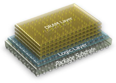
Next generation Game consoles are going to use at a Min 2.5D and I expect the PS4 will use 3D stacking. 1st Xbox720 will use at least 2.5D and possibly the new IBM 3D wafer stacking coming on line in 2013. Only from the Oban name and it's AMD GPU being made in a different factory (to be "Fused" together in the same package with CPU) along with both the PS4 and Xbox720 both using a AMD GPU makes me think that both the PS4 and Xbox720 will be 3D stacked.
Stacking will change how Consoles are designed. High volume game consoles will be among the first CE equipment to change to full 3D stacking and as with Xbox in the past will share development costs using some of the same wafers designed to industry standards for 3D stacking. The AMD Fusion (X86 CPU-GPU in the same package) is taking advantage of and might be designed to 3D stacking standards which might be what impacted the choice to use the AMD GPU by both Sony and Microsoft. Microsoft has other obvious reasons to stay with AMD but Sony does not...moving from Nvidia to AMD can have the above as a possible reason. Using a 3D stacking standard GPU from the AMD fusion and fusing it with a IBM Power CPU in a 3D stack with memory and more makes sense from the articles I've read. GPUs will have upwards of 2000 shading units and it makes sense to build such a GPU with stacked multiple smaller wafers.
http://www.tezzaron.com/technology/3D_IC_Summary.html
http://www.3d-ic.org/
The 3D-IC Alliance is a consortium of integrated circuit designers, developers, and manufacturers. Its objective is to promote standards for three-dimensional integrated circuits (3D-ICs) in order to accelerate their availability and acceptance. Industry-wide standards would allow virtually any semiconductor vendor to implement 3D technology.
Non-members are invited to join the 3D-IC Alliance. Membership is free! We ask only that you be willing to read and comment on new standards as they appear.
The first standard released by the Alliance is IMIS™ (Intimate Memory Interconnect Standard), available for immediate download on the Standards page. This standard reflects our initial focus on the standardization of vertical interconnect requirements such as pad sizing and spacing, interconnect keepouts, and materials. The Alliance intends to define a family of interconnect standards to accommodate embedded interconnect systems and various methods for adding backside or frontside interconnect. In January of 2010, a press release from SEMI praised IMIS™: "This standard lays the cornerstone for memory-to-logic 3D integration and establishes a basis for future collaborative efforts in the industry."
Other groups are also working toward standards for 3D-ICs, but so far our IMIS™ stands alone. Members and non-members alike are encouraged to develop and submit more 3D-IC design standards for consideration.
The 3D-IC Alliance plans to publish additional specifications for ICs and/or wafers that are designed to be stacked and vertically integrated. Any ICs or wafers that are processed and designed to these standards should be 3D integratable by most (if not all) Alliance members. The Alliance may also work to produce specific protocols and signaling and electrical specifications, allowing broad adoption and interchange between various die-level or wafer-level vendors.
http://www.nist.gov/pml/div683/3d_ic.cfm
Best series of articles on 3D stacking.http://www.electroiq.com/articles/ap/2011/05/rdl-an-integral-part-of-today-s-advanced.html said:3D Integration, where multiple layers of planar devices are stacked and interconnected through the silicon [3]. The resulting decreased chip area results in much shorter global interconnect, which results in less power required to drive signals the shorter distance.
Once the infrastructure is in place, it is hoped that 3D IC technology will reduce both risk and cost through economic benefits such as:
a) reducing the time it takes to design and verify chips at the most advanced nodes;
b) allowing the use of older analog IP blocks rather than having to develop new IP blocks at the most advanced process nodes; and
c) allowing the mixing of normally incompatible technologies (heterogeneous integration).
Three-dimensional technology can enable the integration of current off-chip memory (like L2 cache) onto the processor chip, thereby eliminating some of the slower and higher-power off-chip buses to off-chip memory and replacing them with high-bandwidth, low-latency vertical interconnections. In addition, on-chip memory (embedded) can be fabricated on a separate layer and bonded to the logic functions. Both of these options improve access latency, the former reducing interconnect length from tens of millimeters to tens of microns, and the latter allowing optimization of memory processing on a separate layer.
While stacking of die, such as memory, is made easier by having identical I/O, stacking other chips will require an I/O interface standardization that is not yet in place. In order to mate such die, silicon interposers with RDL (single or double-sided) are used. It is expected that interposers will function as a stop gap until standardization is in place to allow full wafer/die stacking. Recent commercialization announcements of 3D stacked memory have come from Elpida and Samsung. Product announcements using interposers have come from Xilinx (TSMC manufacturing the interposer) and IBM fabricating interposer-based modules for Semtech.
Nemesis121
Member
Look at this link and scroll down to the BOM chart of most of today's graphics cards. http://www.investorvillage.com/mbthread.asp?mb=476&tid=11143553&showall=1
Look at the memory cost of the fastest 2GB GDDR5 for the AMD 6970. That is the level of memory that'll be in the next gen consoles.
Late last year 2GB cost $48 X4= $192 just for 8GB memory. And that is manufacturing cost.
I'd also like to know where I can buy 8GB of GDDR5 for under $100 please!
Newegg sales hahahahahaha, my friend got 16GBs for $60...
Newegg sales hahahahahaha, my friend got 16GBs for $60...
That wasn't GDDR5, dude.
McHuj
Member
7870, despite those slides, eats over 200w. Something Pitcairn-level in a console is going to have to be downclocked or some CUs removed for it to happen.
http://www.hardocp.com/article/2012/03/04/amd_radeon_hd_7870_7850_video_card_review/13
Why are you quoting total system power at the wall as the power of the card??
http://www.techpowerup.com/reviews/AMD/HD_7850_HD_7870/24.html
TechPowerUp uses a high-end multimeter in between the PCI bus, connectors, and card to completely isolate it from the system. They're show 115W for Crysis 2 Extreme benchmark and 144W for Furmark.
Bolded the parts that are patently untrue.The arguments I'm hearing about the # of RAM chips on the motherboard determining maximum RAM haven't been true for a few years as the last Xbox redesign used 2.5D stacking for RAM/CPU and GPU. This reduced chip count, made it more efficient and more reliable. The RAM used was 3D stacked.
Don't want to fight about anything else at this time.
Angelus Errare
Banned
Why would that not be an option on a console?
Would that issue not be resolved by using a Fusion chip where the GPU and CPU are in the same die?
At the same time I wonder, why a console could not have a split ram pool as like a PC does. Shouldn't that solve most issues anyway?
I was about to ask, why not just take the small performance hit and use DDR3 (going by this). But their conclusion reminded me, that more ram does not matter if it ultimately results in lower performance.
GDDR3's highest density is 128MB chips...so you'd need even more to get 8GB than using GDDR5
Bolded the parts that are patently untrue.
Don't want to fight about anything else at this time.
Not really finding anything about stacked ram on the 360 s right now, yeah.
Why is the same topic reheated a billion times? People who don't know that there are different types of RAM technology and are like "lolz I can get 32GB RAM for free from the Turkish bazar" should not participate in this discussion.
I believe even 2GB is close to a best-case-scenario.
I believe even 2GB is close to a best-case-scenario.
jeff_rigby
Banned
Bolded the parts that are patently untrue.
jeff_rigby said:The arguments I'm hearing about the # of RAM chips on the motherboard determining maximum RAM haven't been true for a few years as the last Xbox redesign used 2.5D stacking for RAM/CPU and GPU. This reduced chip count, made it more efficient and more reliable. The RAM used was 3D stacked.
Don't want to fight about anything else at this time.
You are correct, the CPU and GPU are on the same die. The eDRAM is 2.5D stacked onto the CPU and GPU die. GDD3 RAM is off chip. Thanks for the correction.
XCGPU engine
Point remains though without my incorrect reference to the last Xbox360 itteration. 3D stacking is impacting the size of memory chips and we can't go by old packaging models to determine how much RAM will be on a Console Motherboard.
http://news.techeye.net/chips/ibm-micron-claim-breakthrough-in-3d-chips said:12/2011 IBM and Micron claim to have made a significant breakthrough in 3D chip manufacturing, as Micron plans to use IBM's new through-silicon vias, or TSVs, to build a Hybrid Memory Cube (HMC).
TSVs are vertical conduits which connect a stack of chips to allow for extremely fast connections, up to 15 times faster than technology available now. It's IBM's 3D manufacturing that has made the product possible. Parts for the Micron kit will be made at IBM's fab in East Fishkill, New York, using its 32nm high-K metal gate process.
Current top devices typically offer speeds of up to 12.8 GB/s, but Micron's HMC should be able to manage 128 GB/s. On top of that, the HMC runs on 70 percent energy compared to existing devices, and on a small form factor that's about 10 percent the size of traditional memory products.

3D stacked Memory chips are faster/smaller and more energy efficient.
Shin Johnpv
Member
Would that issue not be resolved by using a Fusion chip where the GPU and CPU are in the same die?
At the same time I wonder, why a console could not have a split ram pool as like a PC does. Shouldn't that solve most issues anyway?
I can't say if the issue would be resolved using a Fusion chip. You'd have to get some one a bit more knowledgeable than me to answer that one.
Well the PS3 had a split pool of ram this gen, and it really hindered things. In a console allowing the developer to decide how much of the ram is used for the GPU and how much is used for the CPU seems to be the better choice.
Going by Raistlin here, manufacturing for perhaps just the first year with more than 8 chips and then simplifying seems feasible, doesn't it?
Sure, but the problem here is that higher density GDDR5 ram chips aren't even on the road map yet. So there's no guarantee of them showing up next year. Plus even if they do there's no guarantee on price. They may come out and they may end up costing 4x what you pay for the size down chip.
What your asking is for them to design a console HOPING for an affordable ram density increase to show up in the nick of time. I don't think the console manufacturers would do that. I would imagine they want to build this stuff with known qualifiers. Not hopes and dreams. Hell in 18 months we may have a break through and GDDRX becomes the thing everyone focuses on, and GDDR5 is pushed to the side, never reaching those higher ram densities.
I would imagine they have to design these consoles with what's available, and known to be available tech in mind.
And don't forget that you need a beefier bus to accomodate more. Once you have a beefier bus in place, future cost reduction becomes, again, more complicated. Simple truth of the matter is that we're getting 2GB of high speed memory at most in the 2 2013 boxes.
The only way you'll see more is in some kind of split configuration or if somehow the high density GDDR5 modules come out later this year (which is doubtful, tbh). And why would you want a split with slower memory? You don't really need 2GB of ram for the OS or anything like that. Your silicon is much better spent on EDRam or something.
You're right, I went and looked at those numbers again yesterday and realized the error. Monday morning and all that.
The only way you'll see more is in some kind of split configuration or if somehow the high density GDDR5 modules come out later this year (which is doubtful, tbh). And why would you want a split with slower memory? You don't really need 2GB of ram for the OS or anything like that. Your silicon is much better spent on EDRam or something.
Why are you quoting total system power at the wall as the power of the card??
http://www.techpowerup.com/reviews/AMD/HD_7850_HD_7870/24.html
TechPowerUp uses a high-end multimeter in between the PCI bus, connectors, and card to completely isolate it from the system. They're show 115W for Crysis 2 Extreme benchmark and 144W for Furmark.
You're right, I went and looked at those numbers again yesterday and realized the error. Monday morning and all that.
Krauser Kat
Member
You are correct, the CPU and GPU are on the same die. The eDRAM is 2.5D stacked onto the CPU and GPU die. GDD3 RAM is off chip. Thanks for the correction.
XCGPU engine

Point remains though without my incorrect reference to the last Xbox360 itteration. 3D stacking is impacting the size of memory chips and we can't go by old packaging models to determine how much RAM will be on a Console Motherboard.
3D stacked Memory chips are faster/smaller and more energy efficient.
to expensive and to far away for next gen.
jeff_rigby
Banned
to expensive and to far away for next gen.
http://www.theregister.co.uk/2011/10/07/hybrid_memory_cube_consortium/
Oct 2011 Samsung and Micron, asserting that existing 2D DRAM architectures can't scale enough to meet the needs of higher and higher performance processors and graphics in computers and network equipment, have formed a HMC consortium (HMCC) to specify a standard cube interface. Other members are Altera, Open Silicon and Xilinx. Any adopter, OEM, enabler or integrator is free to join. + IBM
The key to this is the Hybrid Memory Cube (HMC), stacked layers of DRAM, on top of a foundation logic layer, interconnected by vertical pathways, Through Silicon Via (TSV) bonds, resulting in denser memory modules. The two reckon that a single 3D cube has 15 times the performance of a single DDR3 DRAM module, while using up to 70 per cent less energy per bit.
The consortium members expect memory cubes to be tightly coupled with CPUs, GPUs and ASICs in point-to-point configurations. It will provide tools and documentation to describe interface specifications as they develop and help their use. The spec should be delivered next year (2012).
Most memory suppliers are going to support 3D memory, it's ready to be produced and Sony is talking about using it in the PS4.
IBM has been researching 3D stacking since 2007. This is a technology that is coming on line with nearly everyone. 3D wafer stacking by 2013.
Can anyone confirm. I'm just using news articles and PDFs.
jeff_rigby
Banned
So how does one determine how much weight to give to rumors. There is the OBAN rumor:AMD, not IBM.
http://semiaccurate.com/2012/01/18/xbox-nextxbox-720-chips-in-production/
So, time for a little speculation. Oban is being made by IBM primarily, so that almost definitively puts to bed the idea of an x86 CPU that has been floating. We said we were 99+% sure that the XBox Next/720 is a Power PC CPU plus an ATI GCN/HD7000/Southern Islands GPU, and with this last data point, we are now confident that it is 99.9+%
but you don't think it's accurate. Then the PS4 rumor with an AMD fusion CPU-GPU but Sony is talking 3D stacking and the above OBAN name is Japanese for a large oblong coin that can be written on.
Confusion reigns in miss-interpreting Carmaks statement that next generation game consoles would have an AMD Fusion like CPU-GPU and the OBAN looks like a fusion of IBM CPU with AMD GPU. Then there was probably a statement that Sony would go AMD for the PS4...which could again be miss-understood and it too would be a IBM CPU-AMD GPU fusion with most likely SPEs included.
http://www.neogaf.com/forum/showthread.php?t=458527 said:In terms of semiconductors, Tsuruta-san picked out emerging ‘through silicon via’ designs. These stack chips with interconnects running vertically through them to reduce length, raise performance and reduce power consumption.
(Note: it's believed the next Power architecture will be a stacked design. This is also the architecture that has been speculated could incorporate aspects of Cell's design, or a next-gen SPU...). It's due in 2013.
With any rumor you should research quotes by the head of Sony Technology and what the industry is doing. You have to weight guesses based on research and i'd guess 80:20 that X86 is not in the PS4.
Just some food for thought here:
1) The Cell is dead. There are no 2 ways about it, despite the (excellent, btw) digging you've done. You won't have a Cell as a primary processor for anything next gen
2) The rumours have been prevalent for over a year now. The "where there's smoke there's fire" rule applies, and I'd wager that there's an *extremely* good chance you'll get an x86 PS4.
3) Oban is for the XBox, and even then the Xbox could end up going all-x86 for all we know.
tinfoilhatman
all of my posts are my avatar
Like someone mentioned above, go with a split memory pool , 2 Giggs for CPU DDR3 and 2 Gigs for GPU GDDR5?
just curious as to everyone's thoughts on this
just curious as to everyone's thoughts on this
Like someone mentioned above, go with a split memory pool , 2 Giggs for CPU DDR3 and 2 Gigs for GPU GDDR5?
just curious as to everyone's thoughts on this
DDR3 is cheap (and slow, compared to GDDR) but... why? You'd still have the issue of a more complex motherboard and difficulty in bringing costs down later as a result. I'd expect all consoles next gen to have a unified memory pool of fast memory (hence 2GB of GDDR5). Could be wrong, of course, but it's what I expect.
DDR3 is cheap (and slow, compared to GDDR) but... why? You'd still have the issue of a more complex motherboard and difficulty in bringing costs down later as a result. I'd expect all consoles next gen to have a unified memory pool of fast memory (hence 2GB of GDDR5). Could be wrong, of course, but it's what I expect.
I am not really sure what the function of the EDRAM was in 360 but someone told me it aided in the implementation of AA. Thus, are we to see EDRAM of more 10MB be implemented in PS4?
Also, is there a possibility of embedded flash storage dedicated to OS this time around?
AgentP
Thinks mods influence posters politics. Promoted to QAnon Editor.
I am not really sure what the function of the EDRAM was in 360 but someone told me it aided in the implementation of AA. Thus, are we to see EDRAM of more 10MB be implemented in PS4?
Also, is there a possibility of embedded flash storage dedicated to OS this time around?
No EDRAM was a failure for the 360, it will most likely not be around next gen, unless the 720 needs it for BC.
http://www.humus.name/index.php?page=News&ID=309
It's funny how sometimes as technology develops what was originally a good can become a bad idea. EDRAM for video cards is such a thing.
Having worked a fair amount with the Xbox 360 the last 2.5 years I find that EDRAM mostly is standing in the way, and rarely providing any benefit.
For the next generation consoles chances are we want 1080p, full HDR, at least 4xMSAA and probably many want additional buffers for deferred rendering or other techniques. I don't think it will be possible to embed enough EDRAM to fit all for many games, so if you're designing a future console now and are thinking of using EDRAM, please don't. Or at least let us render directly to memory. Or only let the EDRAM work as a large cache or something if you really want it.
No EDRAM was a failure for the 360, it will most likely not be around next gen, unless the 720 needs it for BC.
http://www.humus.name/index.php?page=News&ID=309
That burned my retinas (dat colour combo). But thank you for scouring the net to find the article.
Put me in the camp that believes we'll get 2GB max next Gen. Even if a company could use stacking to store more chips, why eat the extra cost when it won't be properly utilized by 80% of the software released?
The edram in the 360 is mostly used to get around the bandwidth issues for current Gen systems. While it does offer benefits for AA and alpha effects, it also has its drawbacks such as tiling being a requirement when the backbuffer can't fit in the edram.
We likely won't be seeing it in a next Gen system outside of the Wii-U.
So based on one developer, it was a failure? Opinions will vary depending on the developer and their needs. MS just made a mistake of designing it so you have to use it.
I am not really sure what the function of the EDRAM was in 360 but someone told me it aided in the implementation of AA. Thus, are we to see EDRAM of more 10MB be implemented in PS4?
Also, is there a possibility of embedded flash storage dedicated to OS this time around?
The edram in the 360 is mostly used to get around the bandwidth issues for current Gen systems. While it does offer benefits for AA and alpha effects, it also has its drawbacks such as tiling being a requirement when the backbuffer can't fit in the edram.
We likely won't be seeing it in a next Gen system outside of the Wii-U.
No EDRAM was a failure for the 360, it will most likely not be around next gen, unless the 720 needs it for BC.
http://www.humus.name/index.php?page=News&ID=309
So based on one developer, it was a failure? Opinions will vary depending on the developer and their needs. MS just made a mistake of designing it so you have to use it.
Put me in the camp that believes we'll get 2GB max next Gen. Even if a company could use stacking to store more chips, why eat the extra cost when it won't be properly utilized by 80% of the software released?
The edram in the 360 is mostly used to get around the bandwidth issues for current Gen systems. While it does offer benefits for AA and alpha effects, it also has its drawbacks such as tiling being a requirement when the backbuffer can't fit in the edram.
We likely won't be seeing it in a next Gen system outside of the Wii-U.
So based on one developer, it was a failure? Opinions will vary depending on the developer and their needs. MS just made a mistake of designing it so you have to use it.
With regards to Tiling method of rendering, is it the reason why PS3 games have V-sync for most third party games as opposed to 360?
brain_stew
Member
Put me in the camp that believes we'll get 2GB max next Gen. Even if a company could use stacking to store more chips, why eat the extra cost when it won't be properly utilized by 80% of the software released?
The edram in the 360 is mostly used to get around the bandwidth issues for current Gen systems. While it does offer benefits for AA and alpha effects, it also has its drawbacks such as tiling being a requirement when the backbuffer can't fit in the edram.
We likely won't be seeing it in a next Gen system outside of the Wii-U.
So based on one developer, it was a failure? Opinions will vary depending on the developer and their needs. MS just made a mistake of designing it so you have to use it.
Humus isn't "just one developer."
With regards to Tiling method of rendering, is it the reason why PS3 games have V-sync for most third party games as opposed to 360?
No, why a game does or does not have v-sync should be determined on a game by game basis IMO.
This link may help with some questions on the subject:
http://www.microsoft.com/download/en/details.aspx?displaylang=en&id=28113
Humus isn't "just one developer."
I never meant to imply nor did I actually say he was "just" one developer. I'm just saying that there is no ultimate/difinitive answer for some things in game development. There have been comments from devs on the benefits of edram as well but their opinions wouldn't apply to all.
This isn't really the thread for this, and I really didn't mean anything major with that post. I just find blantant comments that are broadly swept across the whole industry silly.
east of eastside
Banned
So how does one determine how much weight to give to rumors. There is the OBAN rumor:
http://semiaccurate.com/2012/01/18/xbox-nextxbox-720-chips-in-production/
Charlie tweeted yesterday the following relating to these rumors:
https://twitter.com/#!/CDemerjian/status/176837612361875459
Just got two independent confirmations about my PS4 x86 article.
In response to me about Microsoft's use of PowerPC:
https://twitter.com/#!/CDemerjian/status/176850408038346752
99+% sure it is, but not 100%
though he refuted any notion of the use of ARM for 720:
https://twitter.com/#!/CDemerjian/status/176911773599924225
I laughed at the sheer ignorance behind those comments then, I again laugh now.
With regards to Tiling method of rendering, is it the reason why PS3 games have V-sync for most third party games as opposed to 360?
Most devs use smart v-sync on 360. Tiling has very little to do with it since the entire frame is stitched together in main memory before being sent to the video out pipeline. The main impetus is really just having better latency when the framerate does drop. They also don't go and spend memory on an extra buffer.
tinfoilhatman
all of my posts are my avatar
The edram in the 360 is mostly used to get around the bandwidth issues for current Gen systems. While it does offer benefits for AA and alpha effects, it also has its drawbacks such as tiling being a requirement when the backbuffer can't fit in the edram.
We likely won't be seeing it in a next Gen system outside of the Wii-U.
Too bad wasn't EDRAM one of main reasons why the 360 had superior AA in most cases?
Like someone mentioned above, go with a split memory pool , 2 Giggs for CPU DDR3 and 2 Gigs for GPU GDDR5?
Well, in your example, you're looking at a minimum of 12 chips (8x2Gb GDDR5, 4x4Gb DDR3). I'd rather spend the extra four chips on more GDDR5 whilst unifying the memory space and simplifying a ton of the hardware design.
If you look back at the PS3, the split memory pool was out of necessity due to Cell and G71 being designed for two different memory technologies and having relatively little time to really come up with a proper unified pool. nV/Sony also had to add a separate XDR interface to RSX so that they could actually get decent bandwidth there. Note how cell has absolutely shit bandwidth to GDDR3 (16MB/s)... There's a lot of wiring needed from each chip to each memory pool if you want the bandwidth from each pool usable by a particular chip. Obviously that gets simplified in a Fusion-type design, and at that point you might as well be using a single memory technology anyway.
Split memory pools with all the integration on the motherboard just doesn't make a whole lot of design sense. If you have a shit ton of wiring to do, you can end up with crazy long routes on the motherboard or resort to adding multiple layers for wires to travel through instead so that you could pack the chips closer together on the 2D layout of the board.
"Maybe" it's not so bad, but the alternative is just simpler.
I was about to ask, why not just take the small performance hit and use DDR3 (going by this). But their conclusion reminded me, that more ram does not matter if it ultimately results in lower performance.
GDDR3's highest density is 128MB chips...so you'd need even more to get 8GB than using GDDR5
DDR3, not GDDR3.
 DDR3 has 4Gbit density chips already. There is 8Gbit as well, but at that point you're trading clocks for density. DDR3 is slow enough as it is.
If >4GB is so important that you're willing to go with a slow speed, then I'd hope for a big chunk of eDRAM to complement it, but then you're sort of splitting the CGPU perimeter between the eDRAM I/O and the DDR3 (just like 360 does with GDDR3 and its eDRAM).
It would just be so much simpler to have a UMA 256-bit GDDR5 bus and not worry about tiling. Sure that makes reducing the size of a GPU harder, but the goal seems to be a combined CPU/GPU anyway, which naturally boosts the area of the digital circuitry and still makes a wide-bus feasible.
Decisions decisions...
DDR3, not GDDR3.
If >4GB is so important that you're willing to go with a slow speed, then I'd hope for a big chunk of eDRAM to complement it, but then you're sort of splitting the CGPU perimeter between the eDRAM I/O and the DDR3 (just like 360 does with GDDR3 and its eDRAM).
It would just be so much simpler to have a UMA 256-bit GDDR5 bus and not worry about tiling. Sure that makes reducing the size of a GPU harder, but the goal seems to be a combined CPU/GPU anyway, which naturally boosts the area of the digital circuitry and still makes a wide-bus feasible.
Decisions decisions...
Faster RAM is more preferable to slower RAM despite size. I am pretty sure they will not be going DDR3 route as it may only hinder in the integration of GPU (AMD R7XXX) which was designed with GDDR5 in mind.
Death Dealer
Member
The only remotely possible way it would have DDR-3, is if that cache is separate and additional to, a large chunk of unified GDDR-5 dedicated to the game program and graphics. It could be a bank for running the O/S or other background functions. But it's a long shot. I always said 2-4GB tops, I think 3GB unified GDDR-5 would be ideal but 2GB is the most likely outcome.
People asking for 8GB are absurd. For the life of me, I don't even know what a game console would do with that much ram. 2GB should be enough. For a max res of 1080p, the developer could have anywhere from 1 to 1.5GB to dedicate to video, depending on how much the game program itself takes up.
I don't think 2GB will be a situation like how the X360 would have turned out to be dramatically gimped if it had shipped with 256MB.
I'm really expecting PS4 to be as good or (hopefully) better than PS3 was back in 2006, at a more acceptable launch price. Ditching the expensive proprietary silicon is a smart move. And a fast BD drive will be cheap as chips.
The only remotely possible way it would have DDR-3, is if that cache is separate and additional to, a large chunk of unified GDDR-5 dedicated to the game program and graphics. It could be a bank for running the O/S or other background functions. But it's a long shot. I always said 2-4GB tops, I think 3GB unified GDDR-5 would be ideal but 2GB is the most likely outcome.
People asking for 8GB are absurd. For the life of me, I don't even know what a game console would do with that much ram. 2GB should be enough. For a max res of 1080p, they should have anywhere from 1 to 1.5GB to dedicate to video, depending on how complex the game itself is. Next gen FPS vs bloated TES VI.
I don't think 2GB will be a situation like how the X360 would have turned out to be dramatically gimped if it had shipped with 256MB.
I'm really expecting PS4 to be as good or (hopefully) better than PS3 was back in 2006, at a more acceptable launch price. Ditching the expensive proprietary silicon is a smart move. And a fast BD drive will be cheap as chips.
Sony does have a history of fuc.... errr.. splitting up the RAM pool. They have done in all their consoles so far. I really hope they don't do that this time around. Let the devs decide how much RAM to use for what.
jeff_rigby
Banned
Just some food for thought here:
1) The Cell is dead. There are no 2 ways about it, despite the (excellent, btw) digging you've done. You won't have a Cell as a primary processor for anything next gen
2) The rumours have been prevalent for over a year now. The "where there's smoke there's fire" rule applies, and I'd wager that there's an *extremely* good chance you'll get an x86 PS4.
3) Oban is for the XBox, and even then the Xbox could end up going all-x86 for all we know.
It's possible that there will be no Cell type SPU in the PS4 CPU IF the next generation Power PC is fast enough and can emulate a SPU. This interpretation of rumors would support "Cell is Dead" but allow backward compatibility.(Note: it's believed the next Power architecture will be a stacked design. This is also the architecture that has been speculated could incorporate aspects of Cell's design, or a next-gen SPU...). It's due in 2013.
If this is the case then Sony and Microsoft CPU-GPU might be very very similar if not, dare I say it, identical. If this generation Sony didn't have SPUs then would anyone disagree that the PS3 and Xbox360 CPUs would have been identical? Now with CPU-GPU in the same package and No SPU....identical? One combination CPU-GPU would lower costs due to economy of scale. Down the road with die shrinks...they would happen more often again due to both sharing costs. Lots of economics in this.
IT also might tie into some rumors that have suggested both Microsoft and Sony have something in common due to the publishing of a domain name Microsoft-Sony.com
And this is speculation based on rumors that might all have some truth in them. My interpretation is trying to find some common ground where all could fit in some way. All arguments about Sony wanting an easier to write for hardware would apply even more IF all next generation are PowerPC/AMD not X86.
Also as the last few excellent posts have pointed out GDDR5 and most likely a unified pool is also probable. 2 Gigs minimum possibly but not likely more...outside the CPU-GPU package?
What does the AMD Fusion include...why is there an advantage:
Change X86 in the quote above to Power PC and eliminate features used only in PCs.http://www.tgdaily.com/hardware-features/50040-cpu-gpu-apu said:AMD to support Fusion APU architecture, as it combines multi-core x86 processing, memory controllers, a PCI-E interface and massively parallel GPU computing on a single piece of silicon.
"The APU includes hundreds of parallel processing cores that can be [used] for HPC applications through the OpenCL programming framework. Unlike conventional GPU server architectures, APU parallel multiprocessors share the same physical memory space with CPU cores," Pokorny explained.
"As a result, the programming model for APUs is simpler, bottlenecks for data movement between GPU and main memory are avoided and data duplication is eliminated.
Senior AMD VP Rick Bergman - who briefly demoed the processor - explained that the APU (Accelerated Processing Unit) combined CPU, GPU, video processing and other accelerator capabilities in a single-die design.
"The Fusion Family of APUs represent a distinctly powerful processing approach to the evolving digital consumer landscape, where more than 28 billion videos are watched each month online and a thousand pictures are uploaded to social networking sites every second," said Bergman.
"This explosion in multimedia requires new applications and new ways to manage and manipulate data. Low resolution video needs to be up-scaled for larger screens, HD video must be shrunk for smart phones and home movies need to be stabilized and cleaned up for more enjoyable viewing."
Hirari said Sony needs to concentrate on Software...with identical CPU/GPU more emphasis will be needed on software as a differentiation. What will the console wars and Fanboys write about <grin>.
If the above is true it could use the IBM 3D stacking but speculation by me of Sony manufacturing custom stacked chips for other CE in the Nagasaki plant using parts out of this is less likely (/XX/ is most likely correct here).
Lagspike_exe
Member
Sony does have a history of fuc.... errr.. splitting up the RAM pool. They have done in all their consoles so far. I really hope they don't do that this time around. Let the devs decide how much RAM to use for what.
It's not that simple. UMA limits the amount of bandwith available, so even though it does make memory managment easier it also creates a bandwith bottleneck.
Clear
CliffyB's Cock Holster
I still say there is less than zero chance that the next Playstation will be x86 based. There are no compelling advantages (why use a general purpose solution for a primarily multimedia focussed system?) and the sheer amount of disruption it would cause to a corporation historically focussed on MIPS/PPC architecture would be very costly.
jeff_rigby
Banned
I agree with you but the AMD Fusion does have multi-media support. So that is not a valid part of the argument. X86 (read current AMD design) is a general purpose CPU which will run hotter and use more energy doing the tasks (games) that a PPC can do. If you are putting both CPU and GPU in the same package this supports, if only for heat, using a PPC. The AMD can't run more than 4 X86 cores at full duty cycle and the OBAN is rumored to have 6 cores (same as one of the AMD Fusion designs). Games often push CPUs to 100% duty cycle but general purpose PC use usually doesn't. The AMD Fusion has hardware support for Codecs and Multi-media support as this is an area that could use large amounts of CPU duty cycle. Then there is backward compatibility.I still say there is less than zero chance that the next Playstation will be x86 based. There are no compelling advantages (why use a general purpose solution for a primarily multimedia focussed system?) and the sheer amount of disruption it would cause to a corporation historically focussed on MIPS/PPC architecture would be very costly.
Sony and Microsoft game consoles will have sales numbers that will be attractive to AMD. Pulling parts out of the AMD X86 Fusion to be used in a PPC AMD GPU fusion is a good possible.
I'm making a big assumption that the GPU choice is the same one as in the AMD Fusion..... The number of shaders or GPU elements as well as any number of other features can be custom but with the basic idea of having GPU and CPU in the same package either on the same silicon (unlikely) or 3D stacked with a common memory buss taking advantage of the Fusion efficiencies.
This needs to be investigated...what did the confirmations say?east of eastside said:Charlie tweeted yesterday the following relating to these rumors:
https://twitter.com/#!/CDemerjian/st...37612361875459 "Just got two independent confirmations about my PS4 x86 article."
I still say there is less than zero chance that the next Playstation will be x86 based. There are no compelling advantages (why use a general purpose solution for a primarily multimedia focussed system?) and the sheer amount of disruption it would cause to a corporation historically focussed on MIPS/PPC architecture would be very costly.
A x86 can be designed very SIMD heavy as can a MIPS/PPC to be very general purpose. In fact most MIPS / PPC designs are very general purpose oriented. All the cpu's Apple used and the Power Line e.g.. There are even examples of them in consoles (Gamecube/Wii). People need to stop thinking x86 is good at this and PPC and this and that and...
These are just ISA's, not microarchitectures, you can basicaly build anything with them.
McHuj
Member
I still say there is less than zero chance that the next Playstation will be x86 based. There are no compelling advantages (why use a general purpose solution for a primarily multimedia focussed system?) and the sheer amount of disruption it would cause to a corporation historically focussed on MIPS/PPC architecture would be very costly.
I wouldn't assume it's a general purpose one. If Sony goes with solution from AMD, it would likely be fairly customized for gaming/media performance (even if it's derived from x86.) I think all the solutions are fairly comparable now a days, in that with enough customization and focus on certain apps (games in this case), they'll all achieve similar performance.
No one ISA will perform a whole order of magnitude better than another so I think the better focus is on what will be cheaper to build and what will be easier on the developers. I also doubt many developers (other than for the Cell's SPUs) code in low level of assembly so they probably don't even see the ISA or care to.
The maximum chip size for GDDR5 RAM is 256MB. 8 of these makes 2GB.
8 chips and all the data lines between them especially if it uses a 256 bit bus or bigger will make the motherboard compex and expensive.
I think in the next generation the'll use two memory pools: a faster one, something around 1,5GB GDDR5 and a bigger and slower one, with GDDR3, for caching and SO purposes.
I think in the next generation the'll use two memory pools: a faster one, something around 1,5GB GDDR5 and a bigger and slower one, with GDDR3, for caching and SO purposes.
I was thinking that's a possibility. Maybe it'd be a better use of resources to squeeze another 256MB of GDDR5 in the board, though (cause your slow gddr3 will still need a slow small bus that could be used for another chip).