• Hey, guest user. Hope you're enjoying NeoGAF! Have you considered registering for an account? Come join us and add your take to the daily discourse.

Next generation Game Console Technology

It all starts here in this 2001 paper outlining the future of the CE industry and digital TV. It continues below with hardware and standards development to support what's outlined in the 2001 paper. Read this 2010 article from AMD, Part the Clouds: AMD Fusion APUs Ideal for Cloud Clients and this continuation of the article. Lots there that applies to us and it's an easy read. After reading think about Zlib having hardware support in AMD APUs and the W3C supporting WebCL and Zlib compression as the standards to be used by web browsers. Think about AMD also including a ARM A5 for DRM and more in their APUs.


Next generation Game Console Technology & PC & Handheld & Super Computer:

1) Fusion HSA and Fabric memory Model Scales from Handheld to Super computer Provides efficiencies to reduce heat and increase performance. (includes OpenCL)
2) Third generation 3D stacking making SOCs affordable (SOCs provide more efficiencies = to two die shrinks, reduce time to market) and here 2012-2013.
3) 3D wafer stacked memory will be ready for Game Consoles 2013-2014 Provides even more efficiencies when inside the SOC.
4) Comprehensive look for faster memory technologies and when they would be ready
5) Early draft of the Xbox 720 & Xbox360 marketing and design (from 2010)
Combine all the above and Next generation Game consoles are possible. It must have the performance of a next generation console and fit in the power envelope as well as be affordable. Many consider this an impossible task. Not discussed is the CPU type or version of GPU.

Cites:

Sony CTO interview on Playstation tech
Article on PS4 leaks parallels Sony CTO interview but adds AMD Fusion
Game Console SOCs shown using 3D stacked/ultrawide with TSVs memory (faster, eventually cheaper & energy efficient) and 3D ultra wide I/O memory
AMD planning 5 years for 3D stacking but not mentioning it.
Video on Fusion by AMD
Heterogeneous computing here now.

Cell vision is like HSA + Fabric computing & very attractive to Sony. Everything in the Sony CTO interview about future Playstation tech has been touched on in the above cites. My opinion is the Cell design was an early attempt at this and much has been developed since. Early Cell is not compatible with current open source HSA & Fabric computing memory model, for this reason we will not see Cell but might see SPUs in some form.

http://eda360insider.wordpress.com/2011/12/14/3d-week-driven-by-economics-its-now-one-minute-to-3d/ said:
According to the data gleaned from presentations by Samsung, Toshiba, AMD, and others, 3D IC assembly gives you the equivalent performance boost of 2 IC generations (assuming Dennard scaling wasn’t dead). Garrou then quoted AMD’s CTO Byran Black, who spoke at the Global Interposer Technology 2011 Workshop last month. AMD has been working on 3D IC assembly for more than five years but has intentionally not been talking about it. AMD’s 22nm Southbridge chips will probably be the last ones to be “impacted by scaling” said Black. AMD’s future belongs to partitioning of functions among chips that are process-optimized for the function (CPU, Cache, DRAM, GPU, analog, SSD) and then assembled as 3D or 2.5D stacks.
This is starting in 2012 with full production scheduled for 2013. It makes sense given standardized building blocks mentioned above in the quote to have a design tool in place to make a blank substrate (Oban) with bumps and traces to allow the building blocks to be attached. This can reduce the time to market and allow for tweeking the design which must be the case as there are rumors of the Oban 720 chip being produced Dec 2011 but redesign rumors last month. This is not possible any other way.

OBAN Japanese Coin


hist_coin13.jpg


The idea of the OBAN, a large blank substrate, to produce a large SOC. It can be custom configured and could be used in the PS4 and Xbox 720. This plus standardized building blocks produced by the consortium make sense. It makes sense of the various rumors. Arguments that this would be ready for this Cycle 2013-2014 have supporting cites.

Old design and assembly methods for SOC with their associated lead times no longer apply. 3D and 2.5D stacking is making large Chips like Memory and FPGA economically practical by splitting up the chip into smaller parts that are checked before assembly in a 3D stack or on 2.5D substrate.

Edit: Going through the SimiAccurate forum and found this:
http://semiaccurate.com/forums/showpost.php?p=158494&postcount=139 said:
AI technique such as Neural Network(image, handwriting recognition) and Genetic Algorithm(optimization used in planning) basically performs searches in parallel. AI techniques are best implemented in a system with many cores. A 1K nodes Neural Network or a Genetic Algorithm with 1K population size will perform 1K searches in parallel. These algorithms do not need a lot of memory. 100MBytes of memory is should be more than enough. What AI algorithm needs is more processing cores.

Currently, the GPU and CPU does not have a common address space. The algorithm needs to move the memory between the GPU and CPU many times during the execution. The memory swaps make implementation of AI on GPU not very efficient. Once the GPU and CPU share the same memory space, it will be very efficient to implement AI on GPU.

If GPU and CPU share the same memory space in Kaveri, Kaveri will have great impact how software is implemented. AI, Computer Vision and linear programming implemented on GPU will be many times faster than implemented on CPU. There will be alot more AI and Computer Vision application on the laptop.
The PS4 SOC should have 100 megs or so of VERY VERY fast "common" memory in the SOC. It's possible to have more, to have the entire system memory in the SOC. This is not likely though if the second GPU is external and also Full HSA using a GDDR memory buss rather than PCIe.

http://www.forum-3dcenter.org/vbulletin/showthread.php?p=9241544#post9241544 said:
Spec numbers that IGN posted are from first/early dev kits that have been replaced in mid January. Now I repeat what I know is based on second dev kits that DO NOT represent the final product. Kits will mosT definitely change. Before I reveal SOME of the specs let me tell you that based on what we have heaRd in our studio from our publisher is that Sony was undecided if they should go for a high end machine and take On MS or go for 1.5 leap.

According to rumors a couple of Sonys first party studios are asking for high end machine to make games that are going to have noticeable generation leap. While Hirai and other heads over in Japan think it's time to think about profitability. For now "fight" is some where in between, edging more towards higher end. RAM has been raised from 2GB to 4GB when most of bigger publishers and first party studios that have saying went mental.CPU yes it is true Sony is moving away from the CELL. Will there be BC? Our publisher doesn't care and we haven't heard a word about it. Again since these are dev kits we can't know more than that 99% ceLL is done and dusted. Second dev kit uses APU design AMD A8-3870k redesigned to have HD 6850 on board. And yes SI rumors are true. APU is paired with the HD Radeon HD 7900. No HDD rumors are untrue since it has aLready been confirmed that just like PS3, every "Orbis" SKU will have large HDD since Sony is very eager to make Orbis the media hub. O and one more thing Orbis will support 4 layer BR discs from day 1."
"Orbis will support 4 layer BR discs from day 1" most likely means that Orbis will be a 4K blu-ray player also (4 layer + h.265= 4K Blu-ray) All PS3s can support 4K video but only Slim blu-ray drives may be able to read 4 layers. (To not fragment the PS3, Sony may not enable 4K blu-ray on the PS3.)

http://semiaccurate.com/forums/showpost.php?p=164227&postcount=225 said:
That's why I keep posting 2.5D stacking news released by the company that Charlie's "Far Future AMD GPU Prototype" picture originated from. Moreover, Charlie made it rather clear that SONY is going for a "multi-chip-on-interposer" HSA design that is supposed to be gradually integrated into a cheaper, monolithic SoC later in the life cycle. We also heard about "two GPUs", so its probably going to be APU + dedicated GPU - with the APU-GPU basically reserved for GPGPU computation.

"Interposer inclusion defines the 2.5D approach. It will route thousands of interconnections between the devices. Coupled with true 3D stacked die (enabled by TSVs), the high routing density and short chip-to-chip interconnect ensures the highest possible performance while packing as much functionality as possible into the smallest footprint.

Functional blocks may include a microprocessor or special purpose logic IC (GPU, applications processor, ASIC, FPGA, etc.) connected through high-speed circuitry to other logic devices or memory (DRAM, SRAM, Flash) ..."
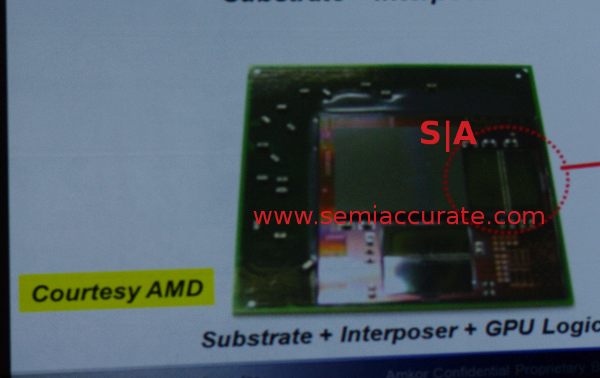
Stacked Memory plus GPU plus substrate. Two of the 4 CUSTOM memory chips are in the red dotted circle (could be total 256 or 512 bit wide). This is the same 2.5D substrate + Interposer technology we will probably see supporting the PS4 SOC just with PS4 SOC much LARGER. It also looks like the following picture includes Southbridge. Just missing the CPUs and MMU for CPU and it would be a APU including memory.

AMD_Interposer_SemiAccurate.jpg


AMD Process Optimized building blocks includes custom memory (from AMD) and cites I posted confirm Micron developed Custom memory for AMD to include in next generation game consoles; the picture confirms Stacked memory, most likely 256 or 512 ultra wide I/O. Stacked memory in the PS4 SOC is possible, the picture proves it.

Arguments? All the above are hindsight, developed in various discussions on NeoGAF with very good criticisms and supported with cites. My opinion is that AMD and Foundries need game console volumes to kickstart the new technologies and Game consoles need the new technologies to make them practical.

1) microsoft-sony.com
2) digitimes PS4 rumor (Must be a PS3 that was confused with a PS4)
3) Leaked Xbox 720 powerpoint document from 9/2010 which has the Xbox 361 coming this 2012 season. IF Oban 12/2011 then 9/2010 was after it was in the pipeline to be produced.
4) This patent and the timing in both filing and publishing XTV game support.
5) Both ps3 and Xbox 360 refresh must have a price reduction built in to allow a price reduction when the PS4 and Xbox 720 are released. This is already possible for the Xbox 360 but the PS3 would NEED a massive redesign to put both CPU and GPU on the same silicon.
6) Sony 2010 1PPU4SPU patent
7) Elizabeth Gerhard's Projects (IBM employee) and an International project involving the Xbox 360 @ 32nm and NO design work for a PS3 refresh at 32nm
8) Oban = large blank Japanese Coin => Is Oban for both the PS3 and Xbox 361 (Microsoft making the chip for Sony using 1PPU3SPU CPU packages instead of just PPUs )
9) Both having browsers at the same time for the first time ever and both have a refresh at the same time for the first time ever
10) Sony depth camera patent (Timing, 9/2011 & again 2/2012)
11) Khronos Openmax 1.2 (Supports Gstreamer-openmax and camera, second Khronos Pdf mentioning Augmented Reality starting Sept 2012 leveraging the browser libraries
12) ATSC 2.0 *-* starts May 2012 thru 1st quarter 2013. *-* h.265 published for use Jan 2013. *-* Sony Nasne *-* RVU support for the PS3 announced by Verizon and Direct TV
13) Energy Star third tier game console voluntary requirements
14) Information on Next generation game console technology
15) Tru2way RVU and the Comcast RDK


http://pc.watch.impress.co.jp/docs/2009/0226/kaigai492.htm
Feb 2009 : Sony investigating two PS4 options Super CELL and Larrabee

http://pc.watch.impress.co.jp/docs/column/kaigai/20091224_339258.html
Dec 2009 : Sony picks Super CELL option for PS4.

http://pc.watch.impress.co.jp/docs/column/kaigai/20100309_353492.html
March 2010 : Additional Description of Super CELL. Interestingly, Sony was most serious about going Larrabee.

http://pc.watch.impress.co.jp/docs/column/kaigai/20120608_538586.html
June 2012 : Super CELL plan died by the end of 2010. SCEI picks AMD in 2011.

________________________________________________________________________________________

"For future reference, the next links a that are merely quotes of Jeff Rigby will be deleted without comment and result in infractions or temp-bans." on Beyond 3D.
 
http://linux.slashdot.org/story/12/06/20/2046233/amd-to-open-source-its-linux-execution-compilation-stack said:
"According to Phoronix, AMD will be open-sourcing its Linux execution and compiler stack as part of jump-starting the Heterogeneous System Architecture Foundation. The HSA Foundation was started earlier this month at the AMD Fusion Developer Summit and AMD plans to open up its stack so that others can utilize the code without causing HSA fragmentation. This will include LLVM code, the HSA run-time, an HSA kernel driver for Linux distributions, an HSA assembler, and other components."

PS4 rumored to have other OS Linux support and at PS4 release a firmware update to the PS3 will enable Other OS Linux support.

http://sonyps4.com/os-support-feature-banned-and-the-ps4/

Insiders from Sony say they have introduced a customized kernel version rather than using the basic kernel to support this feature. This customized kernel may support specific versions of Linux only as a part of beta testing. Subsequently Sony will enable all version support after successful completion of beta testing.

But this time Sony is confident that they won’t block this feature, and that they have an alternative to block the security threats.

An inside source also says Sony’s firmware upgrade during the release of PlayStation 4 will re-enable the other OS support in PlayStation 3 as well. So it’s good news for PlayStation 3 owners too after suffering for couple of years. Moreover it’s believed to be a gamble to boost PlayStation 4 sales.
The first part, providing Linux support as Other OS in the PS4 makes sense as it did with the PS3, an effort to expose heterogeneous computing and Cell and with the PS4, to expose AMD's Open Source HSA and OpenCL to as many programmers as possible.

The second part, enabling other OS support for the PS3 would be a marketing (sales) effort or perhaps support for Linux.

Intel is behind Wayland/Westin 1.0 composition layer (using Cairo) instead of Xwindows due in a few months then GTK rewrites to optionally eliminate Xwindows GDK calls. Latest Linux kernel has now absorbed the Google Android Linux kernel changes that didn't use Xwindows (Tim Bird of Sony) and optimized to support embedded lower resource platforms. Latest Linux kernel is now smaller and faster. Rewrite for Glib to use Android D-Buss routines and more to make it faster and smaller. Combine them all and you have a smaller eLinux platform like Tizen or a optimized Gnome Mobile that can also be used for desktop.

In AMD presentations there are references to DRM (Blu-ray) and built-in control points. A special "simpler" Linux kernel could limit features. I don't know how this will play out.

kaigai6.jpg


2011 "Cell vision" = AMD HSA IL with Fabric computing memory model (common memory address virtual memory model) and JIT compiler. OS has to support this and a simplified Linux kernel could support this in Software which would provide advanced features that would have many Linux libraries as optional components. PS4 and PS3 getting Linux Other OS support at the same time and Google TV more easily supported by the latest Linux kernel makes me believe the "Cell Vision" will be supported by the Linux OS on the PS3 and PS4. AMD says AMD HSA with HSAIL scales from Handheld to super computer and with a new lighter eLinux that can also scale from handheld to super computer it should open up opportunities. (AMD also appears to be going after handheld to super computer markets).

3D consortium "building block" stacking (IBM, Global Foundries/AMD and Samsung) is going to reduce the cost of SOCs allowing even more powerful AV equipment that can run eLinux OSs.....Sony, Samsung, LG, Google, and others know this and are behind the scenes (Tim Bird of Sony, also Intel and Samsung with Tizen) steering Linux to support new opportunities. (Glib is getting some routines replaced by Android routines. Gstreamer and GTK toolkit require Glib support. Gstreamer 1.0 and Glib rewrites may be why Sony has delayed implementing Commercial DASH and is still using AVM+ for non-commercial DASH)

Multiple technologies discussed in 2008 have been developed over the last 5 years and are to be implemented this year. Nov-Dec 2011 saw published news articles including on the Software side Khronos openMax IL 1.2 which was delayed from 2008 till Nov 2011. h.265 is to be published Jan 2013, Webkit is now nearing full HTML5 <video> and WebGL support with Google-Microsoft-Netflix recently proposing a DRM scheme for HTML5 <video>, Gstreamer 1.0 is now ready for release and Sony used Gstreamer in their Google TV.

Take all the future vision statements we have heard since 2004 and re-look at them as everything is just about in place to support most of them. The long delays seen from 2008 have now been explained....it's starting this year.

________________________________________________________________________________________

"For future reference, the next links a that are merely quotes of Jeff Rigby will be deleted without comment and result in infractions or temp-bans." on Beyond 3D.
 
That is amazing, I am officially flabbergasted.

You really did not get even one measly post since 11th of may till today. Even horrible and I mean really horrible OPs seem to get at least one snide comment.

I don't really get much of what was posted though. LOL at linux support reappearing, even if it does, for how long this time?
 
The stacking stuff hasn't even been done at a commercial level by intel at their uber-fabs so far though, right?

Are IBM scheduled to have it mature enough to ship consoles with that silicon in next year, and have the final design ready even earlier?
 
Sony filed a patent for a Method and apparatus for achieving multiple processing configurations using a Multi-processor System Architecture.

Let Me rephrase that; Sony patented a 1PPU and 4SPU module with cache that could be combined with Cache crossover switch into a 4 module HSA Cell (Figure 7).

The design is an updated Cell with only 4 SPUs with a rato of PPU to SPU of 1:4 and no ring cache buss. All the whitepapers I read confirm ratio and 4 SPUs with a common cache as the optimum number before they step on one another with memory access requests.

The PS3 cell design could NOT be included in a AMD HSA SOC but the 1PPU 4SPU modules in the patent could be, may still be in a PS4.

How accurate are the rumors for the PS4? How many SPUs would be needed to emulate the PS3? Are there still plans to add one or two SPU HSA modules? They can't be connected via PCIe, they have to be connected to the main memory buss and that's not going to be a plugin.

These 1PPU-4SPU modules connected to a memory buss were early on not understood. Now with AMD HSA and reading how the 4 X86 CPUs in a AMD fusion are connected to cache and memory we see the same crossover switch as in this patent to connect 4 (1PPU+4SPUs) modules. Further, it appears that Sony was taking the same approach with "Building blocks" that could be used in multiple applications and platforms as AMD is doing with the Consortium and 3D/2.5D stacking.

Sony publishes a patent just before they are going to use it. A Dec 2010 publish fits the 2.5 year lead time AMD/Global Foundries has said they need for custom designs (at least before the New Consortium "building blocks" 3/2.5D stacking coming on line in 2013 which is supposed to reduce time to market and reduce costs to produce SOCs).

The Fusion APU rumored in Developer platforms is nearly identical in CPU performance to the 4PPU 16SPU (figure 7). That tells us that CPU performance for next generation was chosen early on (by both AMD and Sony) to support a CPU bound next generation (UE4) in addition to older GPU bound depending on the second GPU performance.

I'd guess it's all economics....but what if the new 4SPU building block was also to be used in a new Slimmer Slim PS3 with 3D stacked memory (supposed to eventually be cheaper) as well as other platforms. Is that still on? There are many changes in economic equations with Sony going with AMD X86.

Edit: In reading the Sony patent, the "PPU is a new ground up implementation of core with extended pipelines to achieve a low FO4 to match the SPUs." IBM and Sony must have been working on improving the PPU to work with SPUs in 2010.

SYSTEM AND METHOD FOR DATA SYNCHRONIZATION FOR A COMPUTER

not sure if this has anything to do with the PS4 but this Sony patent is using a lot of APU's in what looks like a online sever reminds me of the severs using PS3's
Great find, it ties everything together.

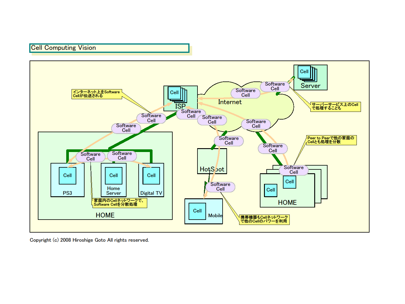
The patent is for both a Gakai like Cloud server and distributed processing 2nd generation Cell Vision - Cell and APU hardware implementation allowing the "Cell Vision" of sharing processor, memory and data over broadband network (Internet and wireless) with a common ISA instruction set. This is the AMD HSA IL (JIT Virtual machine) which "Scales from Handheld to Supercomputer".

The date in the patent is Dec 8, 2011, it starts with Cell in PDAs (1 cell personal handheld devices like cell phones and Tablets), TVs 4 cell...you get the point, as many cell processors (CPU + SPU) as needed by the device and goes on to use Cell and APU as equivalent building blocks Cell=APU=(CPU + GPGPU)=(CPU + SPU).

The Dec 8, 2011 date is important! The first picture with Cell in everything is the original vision with Cell still planned for advanced CE devices displaying 4K (TV and high end 4K blu-ray). Cell is in the Toshiba 4K TV and it does have features not possible without Cell.

Toshiba PDF mentioning the reason for the Cell (power wall, Frequency wall) and applies to Heterogeneous Cell as well as Fusion APU. Also 1 SPU = 16 Intel core Duo X86 processors for single precision FLOPs in 2008.

SPURS engine (4SPUs) designed to be included in platforms with other processors like X86 (Face Recognition, Media codec, Gesture recognition and more). This is now or will soon be provided by GPGPUs in platforms with GPUs. Platforms that need this power but don't need GPUs will probably use Cell (4K TV, 4K Blu-Ray). PDF also mentions clusters of cell over network to share processing, POSIX etc. This is a 2008 "Cell Vision" and the 2011 Sony patent is a later "cell vision" also including a Virtual engine like PS Suite's Mono.

You can reuse your application and library running on SPE across all Cell family processor. All your efforts on one platform are preserved on other platforms.
Please quit &#8220;reinvention of the wheel&#8221;

Please join us to create common environment
Please stop developing environment, but feedback to common environment instead
Please focus on your actual applications
Please look forward to enjoying compatibility
Firstly, write your code using PS3 or CRS(Toshiba&#8217;s Cell Reference Set)
Then, scale up to high performance computing world using QS22 or later blades without any modification
And, make available to PC users using SpursEngine!
Sony created a group to develop and promote DLNA (2000) to share media over the home network. This is being expanded to RVU which is Remote Viewing and control of DVR boxes. DLNA includes discovery and Plug and Play which was developed by the DLNA group. A next generation game console following this vision will need DLNA, RVU and multiple low power standby modes always listening to the Network port; the AMD Fusion SOC chipset provides these as well as the 2011 "Cell vision".

That AMD is including this in all AMD Full HSA Fusion APUs (2013 and later) means the PS4 and future PCs (at least AMD) will be able to share application code and data transparently. I don't know how far this will be taken......it's possible to have the same applications run on PS4 and AMD PCs because of the HSA IL virtual machine. The OS (Microsoft Windows 8? or a simplified Linux with PS3 Linux kernel released at the same time as the PS4 Linux supporting the HSA IL virtual machine?) would have to support this and this is possibly another reason for the domain name registration microsoft-sony.com and sony-microsoft.com. I suspect this will be fleshed out more at the June AMD developers conference and might be hinted by Sony at E3. Will this if properly explained to the consumer impact buying a PS4 over a WiiU. Is the next Xbox supporting this?

Will PS Suite be tied into this at some point in the future (announced one month after the above patent)? OpenCL and HSA IL? The PS3 application side is evolving toward a Gnome Mobile Webkit desktop at least as far as functionality and could support a HSA IL virtual machine.

Read posts here especially 4th down.

http://www.anandtech.com/show/5847/answered-by-the-experts-heterogeneous-and-gpu-compute-with-amds-manju-hegde/3 said:
AMD is addressing this via HSA. HSA addresses these fundamental points by introducing an intermediate layer (HSAIL) that insulates software stacks from the individual ISAs. This is a fundamental enabler to the convergence of SW stacks on top of HC.

Unless the install base is large enough, the investment to port *all* standard languages across to an ISA is forbiddingly large. Individual companies like AMD are motivated but can only target a few languages at a time. And the software community is not motivated if the install base is fragmented. HSA breaks this deadlock by providing a "virtual ISA" in the form of HSAIL that unifies the view of HW platforms for SW developers. It is important to note that this is not just about functionality but preserves performance sufficiently to make the SW stack truly portable across HSA platforms
This starts with AMD 2013 HSA Fusion APUs and the PS4 SOC should be a 2014 design. Speculation but fits Sony & Toshiba goals for Cell and explains Sony going with a AMD fusion APU as the vision is identical and AMD has done the work. Both AMD and Sony need this to succeed. My opinion is Sony is going to concentrate on software and AMD on hardware including hand-helds.....partnership that hasn't been announced yet? AMD/Global foundries is part of the low power ultrawide memory I/O standards group =>handheld memory. <grin> best choice in a AMD HSA Fusion SOC for handhelds.

http://www.pcadvisor.co.uk/news/sof...ec-for-software-use-across-multicore-devices/

ARM, AMD Other companies in the HSA Foundation are Texas Instruments, which develops chips for smartphones, Imagination Technologies, which develops graphics technology used in smartphones and tablets and MediaTek, which provides mobile chips.

The Heterogeneous System Architecture (HSA) Foundation will provide an open hardware interface specification under which program execution can be easily offloaded to other processing resources available in servers, PCs and mobile devices. The new specification will lead to applications that are portable across architectures, while also enabling workloads to be broken up between CPUs and graphics processors for faster and more power efficient computing.
= Cell vision 2011

Software is usually written specific to a device, and the HSA Foundation is an effort to abstract the hardware layer so software can work across the multiple devices and cores, said Dean McCarron, principal analyst at Mercury Research.
For example, smartphones have customized versions of Android, but a standardized specification could provide the groundwork to abstract the hardware, which could enable Android builds to work across different devices.

"It looks to me like they are laying down some of the infrastructure to enable some portability," McCarron said. "If you established what amounts to a standard API for cores, that interaction can be abstracted."
= HSAIL

Offload GPU and CPU processing from your handheld to your PS4....coming with next generation pretty much confirmed. I can't imagine Sony not being a part of this since it echos the 2011 Sony Cell vision patent.

Edit: Here is a AMD patent application for "Device Discovery and Topology Reporting in a Combined CPU/GPU Architecture System " which is the Discovery method for HSA sharing of resources/distributed procesing.

Both Sony and Microsoft patenting distributed processing Microsoft QOS patent of a Xbox 720 serving media and Games to handhelds.
 

injurai

Banned
The stacking stuff hasn't even been done at a commercial level by intel at their uber-fabs so far though, right?

Are IBM scheduled to have it mature enough to ship consoles with that silicon in next year, and have the final design ready even earlier?

Stuffing that cutting edge technology would not be cost efficient for consoles. remember that they know what they are putting into their systems quite early in development.
 

thuway

Member
All I want to know is -

According to your information- how much RAM, and what type of GPU will be used in the PS4?
 

Limanima

Member
Al I want to know is: will the PS4 do 4D? Will the clock be fixed this time?

Now seriously: this stuff looks like chinese to me.
Can someone please translate?
 

StevieP

Banned
I posted this on Beyond3D and will ask this same question here:

How do you guys feel about a large amount of slower memory (such as DDR3) instead of a smaller pool of faster memory (such as GDDR5) powering your next gen consoles?
 
Looks fun, i wonder how they will deal with heat from 3D.
With large surface area and 2.5D thus the Oban large oblong coin reference.

PuppetSlave said:
That is amazing, I am officially flabbergasted.

You really did not get even one measly post since 11th of may till today. Even horrible and I mean really horrible OPs seem to get at least one snide comment.

I don't really get much of what was posted though. LOL at linux support reappearing, even if it does, for how long this time?
It's just a condensed version developed by several people in several threads on NeoGAF. Somewhat technical but all together explains how a powerful and economically practical (inexpensive) game console is now possible.

Sir_Crocodile said:
The stacking stuff hasn't even been done at a commercial level by intel at their uber-fabs so far though, right?

Are IBM scheduled to have it mature enough to ship consoles with that silicon in next year, and have the final design ready even earlier?

injurai said:
Stuffing that cutting edge technology would not be cost efficient for consoles. remember that they know what they are putting into their systems quite early in development.
You missed several points:

1) AMD has been working on the idea of 3D stacking "building blocks" for 5 years. The idea of building blocks means that AMD can choose from a catalog of "Standardized process optimized" building block wafers they can 2.5D attach to a SOC (Oban) substrate and build just about anything to order, reducing time to market and COST!

2) Cutting edge technologies will eventually be cheaper to implement given Testing of building blocks before assembly and economy of scale. Image a PS3 SOC with most of the Motherboard components in one SOC @ 28nm. There would no longer be a need to send the components to China to be assembled; same applies to a PS4.

3) Game consoles with their large volume are the ideal use case for this.

thuway said:
All I want to know is -

According to your information- how much RAM, and what type of GPU will be used in the PS4?
I can't answer that as those choices are NDA and are business decisions by Sony and Microsoft. 2 Gig of memory makes sense if in the SOC, 2 Gig of GDDR5 outside the SOC is the rumor leaked from PS4 developers.

DieH@rd said:
Nothing new appeared on Microsoft front? Rumors of quadore/16 threaded Power7+ are still on?
Don't know anything but wild rumors. Redesign is now easily possible given AMD/Global Foundries/IBM 3D stacking (TSVs) "Standardized building blocks" and software to redesign the Oban SOC substrate so time to market is not as long as before. Rumors of Microsoft changing the design might be reacting to rumors of Sony changing from 4 more powerful X86 CPUs to 2 less powerful jaguar cores and that implies this is somehow more powerful so that Microsoft had to redesign the Xbox3? So I've got wild speculation that the CPU change in the Sony AMD SOC was to make room and allow a power/heat budget to add 1-2 (1PPU4SPU) modules.
 
I posted this on Beyond3D and will ask this same question here:

How do you guys feel about a large amount of slower memory (such as DDR3) instead of a smaller pool of faster memory (such as GDDR5) powering your next gen consoles?
The trend is to more powerful CPU or APU. Stepping back and looking at the most memory intensive feature on this generation is shader libraries. Objects generally have graduated shading due to lighting and surface detail. Present technique is to have libraries of picture assets that are cut and pasted into triangles whose size is selected as a good match for the surface being shaded. Some assets and shader features are now calculated or modified by lighting calculations. What if MOST not all shader assets are math descriptions rather than pixel descriptions in Collada format libraries. Memory size will not be as much of an issue in that case but very powerful and fast CPUs needing very very fast memory will.

Developers should be concerned that all platforms either have near the same CPU performance or more memory. Deliberate leaks and rumors needed to force one or the other platform developer to improve one or the other to allow software developers and easier time porting is to be expected.
 

StevieP

Banned
If Sony is serious about 2014, we need to see 4gb of RAM or more. It seems to be the largest bottleneck.

So you're in the camp that would rather see more slower ram in next gen consoles because it's a higher number, rather than less but faster ram? You may just get your wish.
 

thuway

Member
So you're in the camp that would rather see more slower ram in next gen consoles because it's a higher number, rather than less but faster ram? You may just get your wish.

Hell yes. Faster ram will do amazing things for load times, but lets be honest here- load times are the last thing on my mind when I play my games. I'm sure caching to HD, intelligent game design, and features that are streamed in will rub some of the salt off the wounds.

If you were to put in 8gb of DDR3, instead of 2gb of GDDR5, I would be very happy. However, I'm an ignorant buffoon who studies medicine by trade. I have no knowledge whatsoever in these mind-games you lot play.
 

StevieP

Banned
Bandwidth matters a *LOT* more than just load times, in regards to faster memory vs slower memory.

It's not as much about load times in this case as it is feeding the components without bottlenecking them. Like drinking a thick chocolate milkshake with a WD-40 spray straw.
 

injurai

Banned
You missed several points:

1) AMD has been working on the idea of 3D stacking "building blocks" for 5 years. The idea of building blocks means that AMD can choose from a catalog of "Standardized process optimized" building block wafers they can 2.5D attach to a SOC (Oban) substrate and build just about anything to order, reducing time to market and COST!

2) Cutting edge technologies will eventually be cheaper to implement given Testing of building blocks before assembly and economy of scale. Image a PS3 SOC with most of the Motherboard components in one SOC @ 28nm. There would no longer be a need to send the components to China to be assembled; same applies to a PS4.

3) Game consoles with their large volume are the ideal use case for this.

Oh awesome. I'm not super familiar with the tecnology, but that sounds to incredibly streamline the creation of processors. When the new consoles finally do arrive it will be glorious.
 

blu

Wants the largest console games publisher to avoid Nintendo's platforms.
The trend is to more powerful CPU or APU. Stepping back and looking at the most memory intensive feature on this generation is shader libraries. Objects generally have graduated shading due to lighting and surface detail. Present technique is to have libraries of picture assets that are cut and pasted into triangles whose size is selected as a good match for the surface being shaded. Some assets and shader features are now calculated or modified by lighting calculations. What if MOST not all shader assets are math descriptions rather than pixel descriptions in Collada format libraries. Memory will not be as much of an issue in that case but very powerful and fast CPUs needing very very fast memory will.

Developers should be concerned that all platforms either have near the same CPU performance or more memory. Deliberate leaks and rumors needed to force one or the other platform developer to improve one or the other to allow software developers and easier time porting is to be expected.
Frankly, it took me a few tries to understand what you're saying there. I eventually succeeded though ; )

I think we're quite far from the time when most surface parametrisation maps (i.e. albedo maps, normal maps, specular maps, displacement maps, etc) will be all procedurally generated on the fly, vs generated and stored for reuse (since once you store them for reuse, whether they come from file storage or not is irrelevant - the texture memory is in use).
"but very powerful and fast CPUs needing very very fast memory will" be needed.

What if true the rumor Sony removed the 4 more powerful X86 CPUs in the developer Fusion APU and is replacing them with 2 less powerful Jaguar cores (Handheld low power) to (my take) enable a power/heat budget for 2 (1PPU4SPU) wafer building block HSA compatible CPUs with SPU coprocessors (in Sony Dec 2010 patent). Assume also a 100 meg or so ultra wide memory in the SOC all GPUs and CPUs full HSA with CPUs doing prefetch for GPUs.

There then might be enough CPU power to allow the PS4 to transition to a new shader model where memory size is not as critical or more ray-tracing or any number of CPU intensive rather than GPU intensive functions. This is I believe from two Epic papers the thrust of UE4, more CPU.

Might it give Sony an advantage in Medical imaging and extend the life of the PS4? At (Guess) a cost of $30.00 assuming these 1PPU4SPU building blocks are also going to be used in Sony TVs, Blu-ray players and the PS3 which was the idea in the Sony Dec 2010 patent which could have been modified for the PS4. It's also possible that Cell was dropped totally in favor of AMD APUs as both Cell and APU are mentioned interchangeably in the Sony Dec 2011 patent.

My guess is the AMD building block library is extensive and AMD can make a custom SOC for Sony with very attractive features so going with AMD is a win. Full HSA, HSAIL and the building block feature can additionally allow for dropping into the custom SOC just about any IP by a third party and that includes the 1PPU4SPU Sony modules which were also designed to be HSA building blocks to be assembled into a SOC using the IBM/(AMD)Global Foundries/Samsung standards.

It can go either way and I am not privy to Sony plans but Cell was not dead in 2008 or even the beginning of 2011 (from patents). IF Sony decided to scrap the idea of Cell it would have been after March 2011 (AMD comment). Lead time for the design of building blocks to standards should have a finished design and testing using FPGA or software or a combination by early 2011 (my guess). The PS4 if being released late 2013 will have the SOC chipset made in test yield quantities 3rd quarter 2012.

The idea of HSA and HSAIL combined with a library if building block wafers built to standards that can custom build SOCs with reduced time to market and reduced cost is going to revolutionize the CE industry in ways we can only guess at. It might have changed Sony's plans as it parallels the Cell Vision as seen in the Dec 2011 Sony patent or Sony and AMD have been working on this for years (witness the Khronos support for AMD HSA).

Edit: My guess is X86 processors are necessary in the AMD SOC to support the HSAIL JIT and prefetch for the GPUs. Libraries created by AMD also require the X86 processors to properly use the GPUs as CPUs. Light (Jaguar) X86 CPUs designed for handhelds can perform these tasks as they are just passing pointers and setting up the GPU to do the heavy work. The PPU in the Sony Dec 2010 patent supported AVX, AVX2 might use PPU-SPU routines. And with SPUs in the PS4, Sony can support PS3 backward compatibility.
 

noobie

Banned
What if true the rumor Sony removed the 4 more powerful X86 CPUs in the developer Fusion APU and is replacing them with 2 less powerful Jaguar cores (Handheld low power) to (my take) enable a power/heat budget for 2 (1PPU4SPU) wafer building block HSA compatible CPUs with SPU coprocessors (in Sony Dec 2010 patent). Assume also a 100 meg or so ultra wide memory in the SOC all GPUs and CPUs full HSA with CPUs doing prefetch for GPUs.

There then might be enough CPU power to allow the PS4 to transition to a new shader model where memory size is not as critical or more ray-tracing or any number of CPU intensive rather than GPU intensive functions. This is I believe from two Epic papers the thrust of UE4, more CPU.

Might it give Sony an advantage in Medical imaging and extend the life of the PS4? At (Guess) a cost of $30.00 assuming these 1PPU4SPU building blocks are also going to be used in Sony TVs, Blu-ray players and the PS3 which was the idea in the Sony Dec 2010 patent which could have been modified for the PS4. It's also possible that Cell was dropped totally in favor of AMD APUs as both Cell and APU are mentioned interchangeably in the Sony Dec 2011 patent.

My guess is the AMD building block library is extensive and AMD can make a custom SOC for Sony with very attractive features so going with AMD is a win. Full HSA, HSAIL and the building block feature can additionally allow for dropping into the custom SOC just about any IP by a third party and that includes the 1PPU4SPU Sony modules which were also designed to be HSA building blocks to be assembled into a SOC using the IBM/(AMD)Global Foundries/Samsung standards.

It can go either way and I am not privy to Sony plans but Cell was not dead in 2008 or even the beginning of 2011 (from patents). IF Sony decided to scrap the idea of Cell it would have been after March 2011 (AMD comment). Lead time for the design of building blocks to standards should have a finished design and testing using FPGA or software or a combination by early 2011 (my guess). The PS4 if being released late 2013 will have the SOC chipset made in test yield quantities 3rd quarter 2012.

The idea of HSA and HSAIL combined with a library if building block wafers built to standards that can custom build SOCs with reduced time to market and reduced cost is going to revolutionize the CE industry in ways we can only guess at. It might have changed Sony's plans as it parallels the Cell Vision as seen in the Dec 2011 Sony patent.

I dont know how many lessons Sony have taken from PS3 & PSVITA launches. But i hope they do realise that initially backward compatibility does matter. There was a research on it recently too. So if they go with a custom design 1PPU4SPU Cell on PS4 it will automatically give them backward compatibility. PS3 even being a failure in respect to PS2 does have a very very strong game library and with so many titles like ICO, GOW, MGS n other rescaled to HD i think it will be stupid to let this library go to waste.

Secondly i believe that many PS2 users, who didnot jumped on the PS3 bandwagon might like to jump on PS4 to not only play PS4 games but also PS3 games if they give backward compatibility in PS4.. like those who might have played GOW1&2 or MGS 2 & 3 but didnt play the final act because they went with XBOX might like to play them with PS4..
 
I posted this on Beyond3D and will ask this same question here:

How do you guys feel about a large amount of slower memory (such as DDR3) instead of a smaller pool of faster memory (such as GDDR5) powering your next gen consoles?

I don't know - what would be the advantage of a lot more RAM? Better Textures? What if the PS4 had only 2 GB RAM GDDR5 and the Xbox 720 6 GB, would the developers care at all? I mean would they create unique super-HD-textures for the Xbox only? I doubt that. And afaik, RAM has little influence on effects etc., the effects depend more on the power of the GPU. Considering that some devs said, there will be a lot of 720p games, I am not sure if RAM is that much important. And if the PS4 has a hard disk drive or a fast Blu-ray drive, they can also use streaming.
 

Log4Girlz

Member
Gemüsepizza;38357944 said:
I don't know - what would be the advantage of a lot more RAM? Better Textures? What if the PS4 had only 2 GB RAM GDDR5 and the Xbox 720 6 GB, would the developers care at all? I mean would they create unique super-HD-textures for the Xbox only? I doubt that. And afaik, RAM has little influence on effects etc., the effects depend more on the power of the GPU. Considering that some devs said, there will be a lot of 720p games, I am not sure if RAM is that much important. And if the PS4 has a hard disk drive or a fast Blu-ray drive, they can also use streaming.

Memory speed is important, if it weren't, we would just have a GPU and HDD and do without the RAM.
 

StevieP

Banned
Memory speed is important, if it weren't, we would just have a GPU and HDD and do without the RAM.

Yes, but people also like really big numbers. Look at this forum over the past few years with what gamers are demanding in their consoles. And in order to get to a big number, you have to forego the speedy kind.

So, if it comes down to gddr5, then is 2GB the absolute upper limit for PS4?

Well... unless you decide to increase the motherboard's complexity. You can have as many gigs of GDDR5 as you want if you're willing to eat a lot of money and end up with a board that looks like this:

replica-front.jpg


Or in Jeff's dreams, like this:
Hybrid_Memory_Cube.jpg
 

RoboPlato

I'd be in the dick
Thanks for compiling all of this. I'd fallen way behind in some of the other threads and this really helps parse out what's important.
 

missile

Member
Gemüsepizza;38357944 said:
I don't know - what would be the advantage of a lot more RAM? Better Textures? What if the PS4 had only 2 GB RAM GDDR5 and the Xbox 720 6 GB, would the developers care at all? I mean would they create unique super-HD-textures for the Xbox only? I doubt that. And afaik, RAM has little influence on effects etc., the effects depend more on the power of the GPU. Considering that some devs said, there will be a lot of 720p games, I am not sure if RAM is that much important. And if the PS4 has a hard disk drive or a fast Blu-ray drive, they can also use streaming.
There are lots of physical effects that can consume quite a lot of memory.
But you are right in the sense that lots of memory isn't worth anything
without a broad bandwidth. The power of the GPU, in doing useful work,
depends largely on the memory bandwidth and latency. Given higher bandwidth,
one can utilize large amounts of memory much better. Hint: solving systems
of linear equations, Ax = b, with A large.
 
The Next Generation According to Game Developers

The next generation of consoles starts in 2013, if all goes according to developers’ plans. In an anonymous questionnaire, multiple industry professionals told IGN that they plan to release games for the next Microsoft and Sony consoles before January 1, 2014.

Multiple developers also intend to launch software for an unannounced platform next year
Apple producing a game console next Year?

To further signal the winding down of the current console generation, approximately 60% of respondents have no plans to release games for the Xbox 360, PlayStation 3, or Nintendo Wii after 2013. Of course, this means some 40% intend to keep at current-gen releases after next year. To that point, an anonymous developer told IGN, “I would not be surprised if something atypical cannibalizes the market, maybe even the Xbox 360 itself.”

From a hardware perspective, nearly 80% of respondents said Microsoft’s next console is the easiest to work with, and the overwhelming majority suspect it will be the sales leader over the next five years.
Nintendo Wii U probably hard to use because of the Split screen (LCD handheld controller).

PS4 harder to write for than Xbox8 when the PS4 is a X86 platform and Xbox8 is rumored to be a PPC + AMD GPU? Sony & AMD probably insisting on OpenCL and HSAIL as well as parallel routines (GPU as CPU) being used so another learning curve for developers with an abrupt transition to CPU bound (UE4) Game engine if you want to get the most out of the platform.

Another take would be multiple different CPUs in the PS4 which would require OpenCL as a common language and the other CPU(s) could be PPU + SPU(s) and/or FPGA. Also possible are developers reacting to less memory in the PS4 making it harder to write games.

Xbox8 is probably traditional GPU bound with Kinect & game using traditional CPU resources.
 

noobie

Banned
The Next Generation According to Game Developers

Apple producing a game console next Year?

Nintendo Wii U probably hard to use because of the Split screen (LCD handheld controller).

PS4 harder to write for than Xbox8 when the PS4 is a X86 platform and Xbox8 is rumored to be a PPC + AMD GPU? Sony & AMD probably insisting on OpenCL and HSAIL as well as parallel routines (GPU as CPU) being used so another learning curve for developers with an abrupt transition to CPU bound (UE4) Game engine if you want to get the most out of the platform.

Another take would be multiple different CPUs in the PS4 which would require OpenCL as a common language and the other CPU(s) could be PPU + SPU(s) and/or FPGA. Also possible are developers reacting to less memory in the PS4 making it harder to write games.

Xbox8 is probably traditional GPU bound with Kinect & game using traditional CPU resources.

Interesting comments by developer. I think by the end of the year we will start hearing more accurate rumours about the next gen plans from the big 2.
 
The following is also edited into the first post.

Going through the SimiAccurate forum and found this:

http://semiaccurate.com/forums/showpost.php?p=158494&postcount=139 said:
AI technique such as Neural Network(image, handwriting recognition) and Genetic Algorithm(optimization used in planning) basically performs searches in parallel. AI techniques are best implemented in a system with many cores. A 1K nodes Neural Network or a Genetic Algorithm with 1K population size will perform 1K searches in parallel. These algorithms do not need a lot of memory. 100MBytes of memory is should be more than enough. What AI algorithm needs is more processing cores.

Currently, the GPU and CPU does not have a common address space. The algorithm needs to move the memory between the GPU and CPU many times during the execution. The memory swaps make implementation of AI on GPU not very efficient. Once the GPU and CPU share the same memory space, it will be very efficient to implement AI on GPU.

If GPU and CPU share the same memory space in Kaveri, Kaveri will have great impact how software is implemented. AI, Computer Vision and linear programming implemented on GPU will be many times faster than implemented on CPU. There will be alot more AI and Computer Vision application on the laptop.
The PS4 SOC should have 100 megs or so of VERY VERY fast "common" memory in the SOC. It's possible to have more, to have the entire system memory in the SOC. This is not likely though if the second GPU is external and also Full HSA using a GDDR memory buss rather than PCIe.

http://www.forum-3dcenter.org/vbulletin/showthread.php?p=9241544#post9241544 said:
Spec numbers that IGN posted are from first/early dev kits that have been replaced in mid January. Now I repeat what I know is based on second dev kits that DO NOT represent the final product. Kits will mosT definitely change. Before I reveal SOME of the specs let me tell you that based on what we have heaRd in our studio from our publisher is that Sony was undecided if they should go for a high end machine and take On MS or go for 1.5 leap.

According to rumors a couple of Sonys first party studios are asking for high end machine to make games that are going to have noticeable generation leap. While Hirai and other heads over in Japan think it's time to think about profitability. For now "fight" is some where in between, edging more towards higher end. RAM has been raised from 2GB to 4GB when most of bigger publishers and first party studios that have saying went mental.CPU yes it is true Sony is moving away from the CELL. Will there be BC? Our publisher doesn't care and we haven't heard a word about it. Again since these are dev kits we can't know more than that 99% ceLL is done and dusted. Second dev kit uses APU design AMD A8-3870k redesigned to have HD 6850 on board. And yes SI rumors are true. APU is paired with the HD Radeon HD 7900. No HDD rumors are untrue since it has aLready been confirmed that just like PS3, every "Orbis" SKU will have large HDD since Sony is very eager to make Orbis the media hub. O and one more thing Orbis will support 4 layer BR discs from day 1."
"Orbis will support 4 layer BR discs from day 1" most likely means that Orbis will be a 4K blu-ray player also (4 layer + h.265= 4K Blu-ray) All PS3s can support 4K video but only Slim blu-ray drives may be able to read 4 layers. (To not fragment the PS3, Sony may not enable 4K blu-ray on the PS3.)

http://semiaccurate.com/forums/showpost.php?p=164227&postcount=225 said:
That's why I keep posting 2.5D stacking news released by the company that Charlie's "Far Future AMD GPU Prototype" picture originated from. Moreover, Charlie made it rather clear that SONY is going for a "multi-chip-on-interposer" HSA design that is supposed to be gradually integrated into a cheaper, monolithic SoC later in the life cycle. We also heard about "two GPUs", so its probably going to be APU + dedicated GPU - with the APU-GPU basically reserved for GPGPU computation.

"Interposer inclusion defines the 2.5D approach. It will route thousands of interconnections between the devices. Coupled with true 3D stacked die (enabled by TSVs), the high routing density and short chip-to-chip interconnect ensures the highest possible performance while packing as much functionality as possible into the smallest footprint.

Functional blocks may include a microprocessor or special purpose logic IC (GPU, applications processor, ASIC, FPGA, etc.) connected through high-speed circuitry to other logic devices or memory (DRAM, SRAM, Flash) ..."
Stacked Memory plus GPU plus substrate. Two of the 4 CUSTOM memory chips are in the red dotted circle (could be total 256 or 512 bit wide). This is the same 2.5D substrate + Interposer technology we will probably see supporting the PS4 SOC just with PS4 SOC much LARGER. It also looks like the following picture includes Southbridge. Just missing the CPUs and MMU for CPU and it would be a APU including memory.

AMD_Interposer_SemiAccurate.jpg


AMD Process Optimized building blocks includes custom memory (from AMD) and cites I posted confirm Micron developed Custom memory for AMD to include in next generation game consoles; the picture confirms Stacked memory, most likely 256 or 512 ultra wide I/O. Stacked memory in the PS4 SOC is possible, the picture proves it.

________________________________________________________________________________________

"For future reference, the next links a that are merely quotes of Jeff Rigby will be deleted without comment and result in infractions or temp-bans." on Beyond 3D.
 
As of 7/2012 it should now be obvious that the Oban SOC or wafer produced Dec 2011 by IBM mentioned in these two cites is for a Xbox 361 and possibly a PS3.5.

http://venturebeat.com/2012/01/25/rumor-control-xbox-720-chips-in-prototype-production/
http://www.fudzilla.com/processors/item/25619-oban-initial-product-run-is-real

The OBAN mentioned as being used by IBM to produce the Xbox 720 Xbox 361 can be what it was named for, a blank that is written on or rather a LARGE substrate with bumps upon which 3D stacked and 3D wafers are 2.5D attached. With proper software design tools and standards (IBM, Global Foundries and Samsung) for wafer sub assemblies and Process Optimized SOC building blocks, AMD has been working on this for 5 years, it should be possible to build SOCs to order at reasonable costs.


According to the data gleaned from presentations by Samsung, Toshiba, AMD, and others, 3D IC assembly gives you the equivalent performance boost of 2 IC generations (assuming Dennard scaling wasn&#8217;t dead). Garrou then quoted AMD&#8217;s CTO Byran Black, who spoke at the Global Interposer Technology 2011 Workshop last month. AMD has been working on 3D IC assembly for more than five years but has intentionally not been talking about it. AMD&#8217;s 22nm Southbridge chips will probably be the last ones to be &#8220;impacted by scaling&#8221; said Black. AMD&#8217;s future belongs to partitioning of functions among chips that are process-optimized for the function (CPU, Cache, DRAM, GPU, analog, SSD) and then assembled as 3D or 2.5D stacks.
This is starting in 2012 2011 with the Xbox 361 and PS3 4000 chassis (Speculation). IBM is further along in TSV technology and the rumor has the Oban at 32nm at least for the IBM produced parts that are combined with the AMD parts.

OBAN Japanese Coin


hist_coin13.jpg


In the Microsoft powerpoint the next Xbox is a Xbox 361 with 1080P and HDMI pass-thru (implied multiple low power modes). Low power modes are going to be required within 2 years for California so any recent or near future refresh has to include it. Low power modes would require a complete redesign, it might be simpler to trash the current design and start over.

The above would support speculation that both Xbox360 and PS3 refreshes would take advantage of the AMD plans above given AMD building blocks support low power modes and will be cheaper to use than redesigning older hardware to support low power modes. In this thread is the Sony 2010 patent for a 1PPU4SPU building block that could 2.5D attach to a Oban substrate with AMD GPU, Southbridge and I/O. It's possible that Sony designed these building blocks to be used in AMD SOCs to replace Cell which can not be used. IF both Xbox 361 and PS3 series 4000 are built with AMD building blocks they would be identical except for CPUs. Given Xbox360 uses exactly the same PPUs as PS3 and the domain registration microsoft-sony.com both could be sharing the design costs of a SOC by using the exact same SOC and emulating their older hardware.

This creates some interesting follow on speculation for Backward compatibility if both Xbox720 and PS4 are X86. AMD has a 4 way cross bar switch for CPU packages. In CPU packages for instance, 4 Jaguar CPU cores can be in one package or 1 Bulldozer and FPUs or combinations of these. It looks like multiples of 4 CPU packages with 4 elements in the sub package. Developer platforms have 4 bulldozer cores with FPUs. There is a rumor that this is going to change to 2 packages of 4 Jaguar CPUs and no FPUs. This leaves room for 2 CPU packages which could be 1PPU4SPU CPU packages that can provide BC as well as advanced FPU duties and more.

Xbox361 and PS3 4000 series chassis if made as speculated above could have more memory and be more efficient if running in native rather than emulation mode. This could be an advantage for OS features like Voice and Gesture recognition as well as Cross game Chat for the PS3. Game mode for both would be 100% backward compatible with just faster more accurate OS features.

Last, both Xbox360 and PS3 security keys have been broken. The complete redesign above would require a second Firmware version and an opportunity to re-establish security for both.

Edit:

The following is about 32nm SOI chips being produced for "Gaming" among other uses starting in Dec 2011 at IBM and GF foundries. This is too early and at 32nm not the rumored 28nm for PS4 and Xbox720. My guess is WiiU as well as Xbox361 or PS3 4000 chassis or both. Charlie at SimiAccurate stated that he heard Oban using this node size and process was being manufactured for Microsoft. He speculated/heard it was for the Xbox720 which NOW does not seem likely.

http://www.globalfoundries.com/newsr.../20120109.aspx
http://www.advancedsubstratenews.com...ibms-32nm-soi/


The press release put SOI front and center, saying, &#8220;The technology vastly improves microprocessor performance in multi-core designs and speeds the movement of graphics in gaming, networking, and other image intensive, multi-media applications.&#8221; IBM&#8217;s 32nm SOI technology was jointly developed with GF and other members of IBM&#8217;s Process Development Alliance

The companies' 32/28nm technology uses the same "Gate First" approach to High-k Metal Gate (HKMG) that has reached volume production in GLOBALFOUNDRIES' Fab 1 in Dresden, Germany. This approach to HKMG offers higher performance with a 10-20% cost saving over HKMG solutions offered by other foundries, while still providing the full entitlement of scaling from the 45/40nm node.

The release also notes that the chips rolling off this new line feature IBM&#8217;s embedded DRAM (eDRAM). ASN readers will remember that IBM&#8217;s eDRAM guru Subu Iyer, wrote in ASN about the role that SOI plays therein back in 2006. He noted that while eDRAMs had previously been done in bulk silicon, &#8220;The complexity adder is about half in SOI compared to bulk for deep trench based eDRAMs.&#8221;

Interesting, too, that the announcement cites networking, gaming and graphics. IBM, of course, has its own successful SOI foundry business, and owns the high-end gaming market, fabbing SOI-based chips for the big three: Sony PS3, Microsoft Xbox 360 and Nintendo Wii (and the upcoming Wii U).

For its part, GF has all the AMD SOI-based business, including all the Opterons, the FX and the &#8220;A-series&#8221; APUs &#8211; including the upcoming &#8220;Trinity&#8221; for desktops & high-end laptops, with the new Bulldozer core.
My guess (from reading the articles) is all on one SOI chip @ 32nm that includes IBM Processors, AMD GPU, AMD Southbridge and eDRAM (larger than 10 megs and not dedicated to GPU?) This is 100% doable with little effort for Xbox360 as the Xbox360S refresh was already more than half way to this (it had an updated IBM PPC processor and AMD GPU). An all on one silicon wafer would be cheaper that the Xbox 360S SOC that 2.5D attached eDRAM. The 2010 360S SOC used a newer PPC processor and GPU with custom Southbridge. I expect a 2012 refresh to use even more updated components that increase efficiency and reduce cost, this includes hardware changes that support UMA, Zero copy and might include GPU as CPU.

For PS3 this is not easily possible. Dumb PS3 shrink is not possible due to the Flex I/O and Rambuss connectors on either side of the Cell so a total redesign is needed and RSX was not designed to work on SOI. My guess is to use the design of two of the Sony patent 1PPU4SPU elements and something like the AMD GPU being used in the Xbox refresh SOC. Xbox had to emulate it's old GPU in the Xbox360S SOC refresh which was a multi-chip on substrate more expensive SOC. No reason the refreshed PS3 can't do the same. If this is what's happening for the PS3 then everything is in this Chip made for a PS3 to support Xbox360 as Xbox uses one of the PPU processors for OS duties which can be emulated safely by other hardware. Likely the same or updated southbridge used by the Xbox360S but at 32nm will be in the SOI wafer also.

In the above, there could be differences outside the SOC between Xbox361S and PS3S like wireless G for PS3 and Wireless N for Xbox.
 

Cesar

Banned
According to rumors a couple of Sonys first party studios are asking for high end machine to make games that are going to have noticeable generation leap. While Hirai and other heads over in Japan think it's time to think about profitability. For now "fight" is some where in between, edging more towards higher end.

It's understandable for Sony if they want a lower cost machine and go for more profit early on, but still, their first party studios are such techheads, it'd be a shame if they get stuck on good but not great hardware.
 

manzo

Member
I think it would be a better idea to split this thread for Xbox 8 and PS4. It would be easier to read the tech findings for each console in their own threads?
 
I think it would be a better idea to split this thread for Xbox 8 and PS4. It would be easier to read the tech findings for each console in their own threads?
Both PS4 and Xbox 720 are using the same or similar technology made possible by AMD, IBM and others in the consortium. This is a LEAP in technology that has been in the planning since 2008 by everyone!

Microsoft-sony.com domain registration seems to imply a partnership which I'm speculating is shared R&D and setup costs for Game Console SOCs either Xbox361 & PS3 refreshes coming at the end of this year or Xbox720 & PS4 or possibly both. Differences would be outside the core SOC...memory size, multi-media support etc.
 

klier

Member
This thread will become one epic thread of Jeff talking to himself, until the PS4 launches.

Which means lot of conversation.
 

ekim

Member
Checking some middleware tools providers, I found that Umbra3 is already nextgen-Ready:
What platforms is Umbra 3 available for?

PlayStation 3, Xbox 360, pc, PlayStation Vita and iOS platforms.

We can provide Umbra 3 on other platforms as well on request. Let’s just say we can’t list every platform we have Umbra 3 on…
(http://www.umbrasoftware.com/en/umbra-3/faq/)

Umbra 3 is used for occlusion culling.

The site was updated a few months when WiiU was already announced - so I guess they are talking about nextbox/ps4.
 
jeff_rigby said:
...lot of technical stuff...

Now I know whose advice I will take the time to read when Wii U / next Xbox and PS4 specs will be detailed.
For now I'll go play current gen and don't try to understand all this... too complex, no motivation trying to understand.

Thanks anyway for taking the time to gather all this. I'll follow this thread.
 

ekim

Member
Next middleware with Ps4/nextbox support:
http://www.radgametools.com/bnkhist.htm

Changes from 1.99q to 1.99r (6-5-2012)

Android is now a supported platform!
Added a new secret platform (contact us for details).
On the Wii-U, switched to using the FS API (since FSA has been deprecated). You'll have to update your code, since this call now takes two parameters.
On Wii and Wii-U, allocate the stack space for the async threads from the BinkSetMemory callback.
 
Top Bottom