• Hey Guest. Check out your NeoGAF Wrapped 2025 results here!

The PS5 SSD controller also has a die shot now

LordOfChaos

Member
E-l52_oXoAM-p3C


Not sure how much we can glean out of this one not being a CPU or GPU, but I think that looks like a quad core CPU cluster at the right, 2x2, unless those are some IO blocks like SerDes PHY. And then lots of SRAM banks at the left. There was that Sony patent on SSD controller table lookups in SRAM instead of NAND cache for extra performance.

Made by Marvell. Appears to be called Titania 2.

 
Last edited:
Why is there a big ass crack in the middle? That's not what you call "a beautiful ship shot". Or what do i know.... :messenger_anxious:
I guess some substrates are more resistant than others, also the chip itself could be really thin, I don't see this being the same amount of layers as the main APU, but still beautiful shot.

Shit like this is what do humanity great, other stuff not so much. Sorry for being nerd
 
I've built electronics for a living for 20 years, some day I hope I level up enough to understand any of this, looks like google maps to me lol
 
Last edited:
I guess some substrates are more resistant than others, also the chip itself could be really thin, I don't see this being the same amount of layers as the main APU, but still beautiful shot.

Shit like this is what do humanity great, other stuff not so much. Sorry for being nerd

Thanks for the informative reply. We learn by asking stupid questions sometimes :messenger_tears_of_joy: . I basically do not know what im even looking at tbh, and seeing that crack in the middle while calling the shot beautiful made little sense to me. Also i love nerds you can learn a bunch of shit from them, so don't be sorry :messenger_tears_of_joy:

be-nice-to-nerds-theyll-probably-be-your-boss-one-day-quote-1.jpg
 
Well the 12 channels seem pretty clearly defined by the 12 connectors around the bottom and left edge.

So, ya know, cool. Cerny wasn't lying lol - its got 12 channels connecting to 6 NAND flash dies.
 
I've built electronics for a living for 20 years, some day I hope I level up enough to understand and of this, looks like google maps to me lol

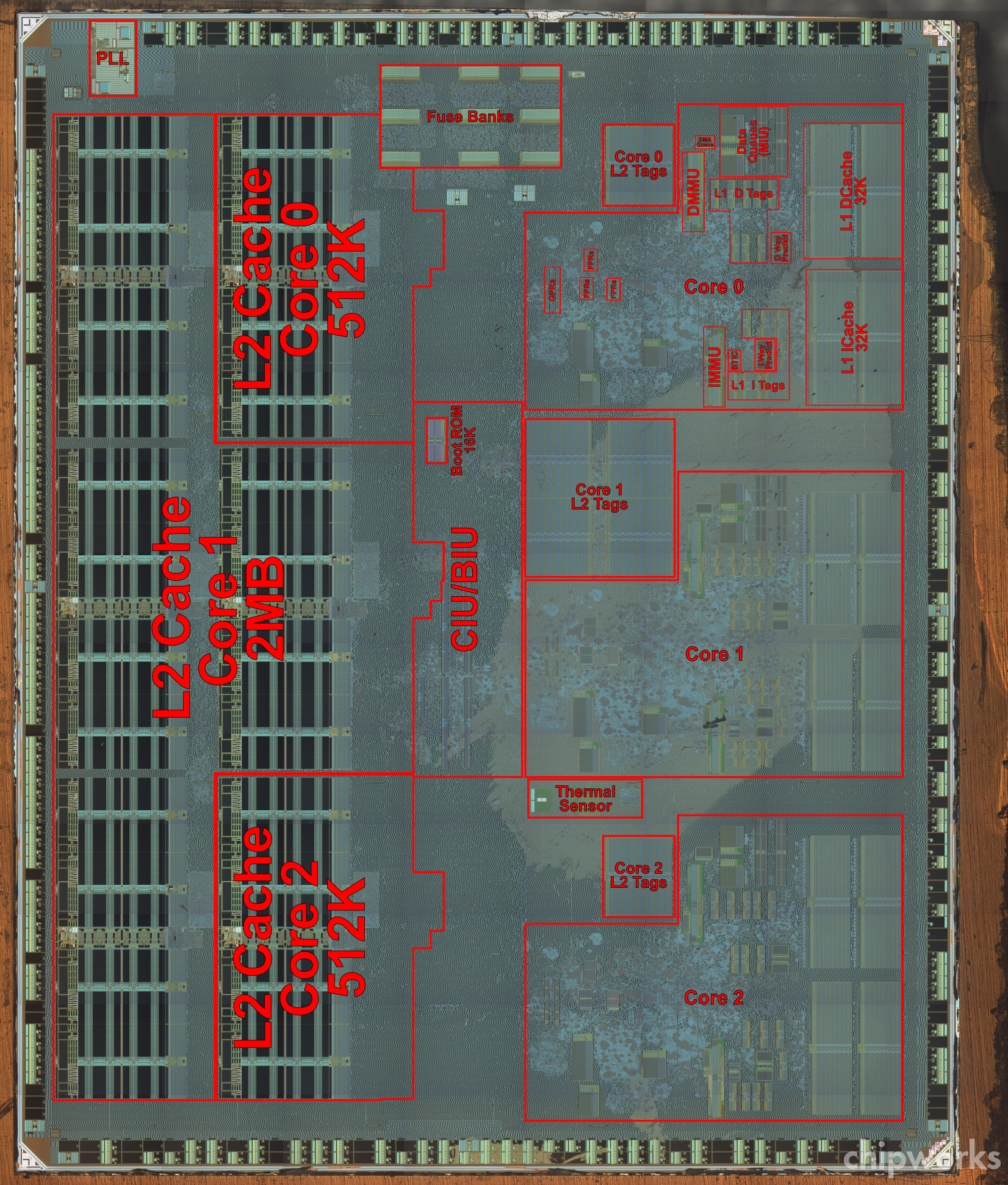
It's not too bad to pick up, you start recognizing things. Here's an annotated Wii U CPU die shot

espresso_annotated.jpg


See where you see the fuzzy city stuff besides straight rows of cache/tags, you're usually looking at a CPU like structure. Where you see straight rows of banks on the left that's SRAM (actually eDRAM in this case but usually SRAM), the fast on-chip memory.

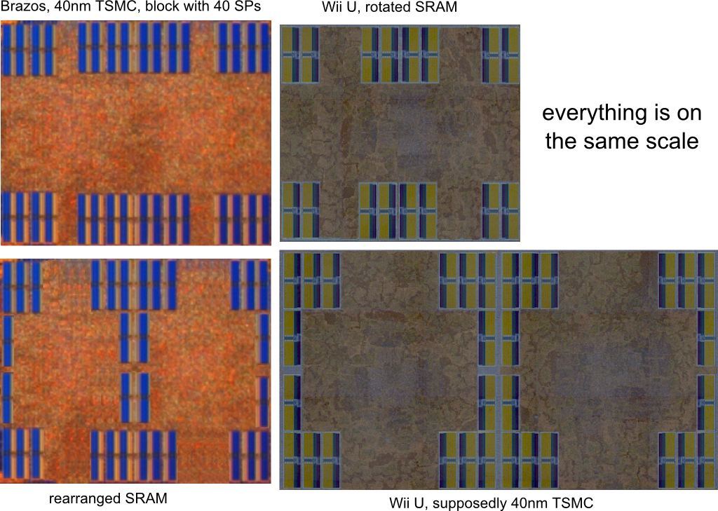
Then on AMD GPUs, the shader engines will look like these cross units

brazos_wiiu_simdfeuev.jpg


Look at a few annotated ones and you start to get it and start to make sense of new ones you look at
 
Last edited:
It's not too bad to pick up, you start recognizing things. Here's an annotated Wii U CPU die shot

espresso_annotated.jpg


See where you see the fuzzy city stuff besides straight rows of cache/tags, you're usually looking at a CPU like structure. Where you see straight rows of banks on the left that's SRAM (actually eDRAM in this case but usually SRAM), the fast on-chip memory.

Then on AMD GPUs, the shader engines will look like these cross units

brazos_wiiu_simdfeuev.jpg


Look at a few annotated ones and you start to get it and start to make sense of new ones you look at
It's just on a whole other level. I look at circuit boards all day but there are a million similar looking components that are doing completely different things. What I don't understand is how the internals can be so similar that a number of xrayed blocks layed out in a certain pattern is the same thing in all APUs.
 
Last edited:
Well the 12 channels seem pretty clearly defined by the 12 connectors around the bottom and left edge.

So, ya know, cool. Cerny wasn't lying lol - its got 12 channels connecting to 6 NAND flash dies.
Did he even ever lied about anything with the PS5?

Machine Learning
Ray Tracing
Extreme Cooling.

Everyone of those things people said he was lying about that actually was true.
 
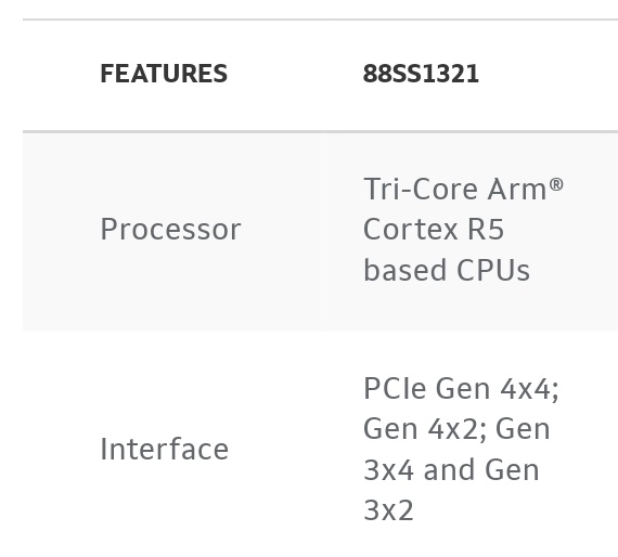
Hmm ok, triple core Cortex R5. The four repeating blocks still look like the cores to me, maybe one is disabled or used for something else/not visible.


E-n6978XsAQ4QCb


Edit: Ok I think I get it, one group of dual cores in redundant lock step operation means one core effectively, second pair ungrouped would mean 3 cores/threads. 8 compute engines each

 
Last edited:
Hmm ok, triple core Cortex R5. The four repeating blocks still look like the cores to me, maybe one is disabled or used for something else/not visible.


E-n6978XsAQ4QCb


Edit: Ok I think I get it, one group of dual cores in redundant lock step operation means one core effectively, second pair ungrouped would mean 3 cores/threads. 8 compute engines each, which is where it equaling many Zen 2 cores for SSD decode comes in.

The Zen 2 cores worth of power is normally associated with the work the I/O complex and the SSD controller are doing together (more the former than the latter)… I do think is more about taking into account the fixed function HW they have added on top of cores and heaps of SRAM.

Even the additional user replaceable SSD takes advantage of the SSD controller and the I/O complex… definitely a good investment there IMHO.
 
Hmm ok, triple core Cortex R5. The four repeating blocks still look like the cores to me, maybe one is disabled or used for something else/not visible.


Edit: Ok I think I get it, one group of dual cores in redundant lock step operation means one core effectively, second pair ungrouped would mean 3 cores/threads. 8 compute engines each, which is where it equaling many Zen 2 cores for SSD decode comes in.


Are the cores really for the decryption? because most pc nvme controllers have arm cores, the phison e18 for example has a controller with 3 arm cores.
 
Are the cores really for the decryption? because most pc nvme controllers have arm cores, the phison e18 for example has a controller with 3 arm cores.

Nah I'm going to remove that line, decompression should rather be in the IO complex as pointed out
 
Last edited:
Top Bottom