both console are incredible ..there's nothing to say about itEven if it's true, look at the Matrix demo.
At the end of the day, it's the games that matter.
-
Hey Guest. Check out your NeoGAF Wrapped 2025 results here!
You are using an out of date browser. It may not display this or other websites correctly.
You should upgrade or use an alternative browser.
You should upgrade or use an alternative browser.
XeSS (Intel ML Upscaling) supported by Series Consoles
- Thread starter Max Payne’s Baretta
- Start date
- News
Loxus
Member
Cerny said PS5 had RT.Using Cerny words and nothing more ...most people should stop fantasizing to what is the GE and its alleged ability to handle meshlets, when Cerny clearly talked about primitive shaders ... the hw support for int4 or 8 (ML) or hw support or vrs hw since none of these things are never mentioned even once by Cerny the others officially .. or some engineers in some private tweets who worked on the development of the PS5 confirmed its non-existence.
It takes consistency
No one believed him.
Cerny said the PS5 SSD is faster them anything on the market at the time he said he.
You did not believed him.
Cerny said the PS5 CPU supports 256-bit instructions.
You believed it had been cut the to 128-bit.
Cerny says the PS5 has RDNA 2 CUs.
You believe it's RDNA 1.
Wired article said in support ML.
Believed it had zero ML capabilities.
I'm sorry, but you guys are fucked up for disregarding official information and have nothing to backup your claims.
Last edited:
I never thought of any of this. Especially with regards to RT. The definition of rdna2 has been used so loosely by AMD, Microsoft and Sony that I'm sure the PS5 GPU can be defined rdna2 given the changes present.Cerny said PS5 had RT.
No one believed him.
Cerny said the PS5 SSD is faster them anything on the market at the time he said he.
You did not believed him.
Cerny said the PS5 CPU supports 256-bit instructions.
You believed it had been cut the to 128-bit.
Cerny says the PS5 has RDNA 2 CUs.
You believe it's RDNA 1.
Wired article said in support ML.
Believed it had zero ML capabilities.
I'm sorry, but you guys are fucked up for disregarding official information and have nothing to backup your claims.
Wired isn't Sony or Cerny
just saying....a 128bit fpu can still process 256bit instructions....(even if that's not the case)
In talking about things that Sony Cerny or other they never mentioned. Meshlets, hw Vrs, int 4/ 8 supp ...These three qualities with the others ...are absolutely part of what defines the rdna2 with respect to the 1
Last edited:
TheRedRiders
Member
Why would your tweets be a better source of truth than curated and published white papers/ articles from NVIDIA, INTEL, AMD ect??
You wanna tell Nvidia that they dont understand mesh shaders ? lmao
there is a reason why the PS5 have the GE and not the mesh shader also if it basically try to do the same things .....have not the vrs, the sampler feedback and probably not the support for int4 and 8..the reason in my opinion isn't "because Sony didn't want it" is because those rdna2 features wasn't ready when Sony choosed their ips
Not my tweets, and LeviathanGamer2 specialises in gaming and hardware architecture at a degree level, you can look through his content and he's respected by some developers and also Alex Battalgia from DF. He's demonstrated his knowledge enough times and he's definitely more reliable than most of the posters on this thread. Also nothing I've said contradicts Nvidia/AMD documentation.
Posters are also getting confused on the nomenclature surrounding "geometry engine", for those who don't know, a geometry engine is a specialised unit found in most AMD GPU's in recent years and it's function is set up and schedule the geometry workloads to the different CU so that's where Primitive and Mesh Shaders come into play. This is also why Mark Cerny mentioned Primitive Shaders as being a more advanced function of the PS5's Geometry Engine.
But before I get accusations of "appeal to authority", lets see what AMD's white papers and ISA have to say about Primitive and Mesh Shaders support at a hardware level:
As I mentioned earlier the hardware changes (to the geometry engine) necessary for Primitive and Mesh Shaders to function were made in AMD's Vega architecture in the NGG fast path, for more details go and read Vega's whitepaper on page 6. Here's the link : https://www.techpowerup.com/gpu-specs/docs/amd-vega-architecture.pdf
RDNA 1 further tweaked and optimised the changes made in Vega and increased the performance of polygon throughput thus increasing the performance of Primitive/Mesh Shaders, go see AMD's RDNA whitepaper for more details: https://www.amd.com/system/files/documents/rdna-whitepaper.pdf
So RDNA 2 which is "where the new Mesh Shaders function", according to AMD documentation and sources there is ZERO changes to the geometry engine and command processors, so no hardware changes were made to facilitate Mesh Shaders. NONE. In fact AMD's ISA make no mention of Mesh Shaders:
Let's also not forget the fact that all of AMD's RDNA 2 cards are converting Mesh Shaders into Primitive Shaders in code and Series X/S will likely be doing this as well, (see LeviathanGamer2's tweet in my original post) this makes sense since both operate the same on a hardware level, the difference is an API implementation.
I'm more than happy to change my mind if you can bring evidence that contradicts this.
If this was true, why do RDNA 1 cards not support Mesh Shaders if it was a simple software fix?
As I've demonstrated as per AMD documentation they can support Mesh Shaders but it may likely be a driver issue.
Last edited by a moderator:
ToTTenTranz
Banned
There's very strong evidence in favour of the PS5 GPU being more-or-less Navi 10 in feature set except with RT hardware acceleration added, very little to support anything else.
Sony: It's an RDNA2 GPU.
AMD: RDNA™ 2 architecture is the foundation for next-generation PC gaming graphics, the PlayStation 5 and Xbox Series S and X consoles.
GAF users: It's Navi 10 and there's little to support anything else.
Yes, save for the official statements given by the companies who designed the RDNA2 architecture and ISA, developed the SoC and its embedded GPU and sell the console in the global market, there's very little information to prove the underlying architecture of PS5's GPU.
I mean what worth are Sony's and AMD's official statements compared to the beliefs of xboxera, windows central and Alex Battaglia?
What makes something a "RDNA2 GPU"? Having RT? Having Infinity Cache? Having VRS? Having AV1 decoding?
The answer is a RDNA2 GPU is whatever AMD tells you it is, because it's just a name.
What actually exists on a hardware level is various IP blocks designed by various teams at AMD, you have people working a ROP, a memory controller, a video encoder/decoder etc. A design team then puts these together on a chip.
The reality is that almost every IP block in the PS5 GPU is very closely related to Navi 10 in what features they support except for the adding of RT acceleration.
Loxus
Member
I never thought of any of this. Especially with regards to RT. The definition of rdna2 has been used so loosely by AMD, Microsoft and Sony that I'm sure the PS5 GPU can be defined rdna2 given the changes present.
Wired isn't Sony or Cerny
just saying....a 128bit fpu can still process 256bit instructions....(even if that's not the case)
In talking about things that Sony Cerny or other they never mentioned. Meshlets, hw Vrs, int 4/ 8 supp ...These three qualities with the others ...are absolutely part of what defines the rdna2 with respect to the 1
The only difference between Xbox Series X/S and PS5 GPU wise is the ROPs.
Everything else is the same.
Architecture is the same.

Compute Units are the same.

It's confirmed officially by AMD that they're RDNA 2.
AMD RDNA™2 architecture is the foundation for next-generation PC gaming graphics, the highly anticipated PlayStation® 5 and Xbox Series X consoles.
AMD says they support Microsoft DirectX Ultimate which means they support the software.
With support for DirectX® 12 Ultimate, the visual pipeline of AMD RDNA 2 is rigged to bring up-leveled immersion through realistic lighting and shadows.
PS5 does not use DirectX API.
DirectX Raytracing, Variable Rate Shading, Mesh Shaders, and Sampler Feedback are all Direct X API features and not hardware names.
But I'm done with this nonsense if official information is being disregarded. The games don't lie.
Loxus
Member
What makes something a "RDNA2 GPU"? Having RT? Having Infinity Cache? Having VRS? Having AV1 decoding?
The answer is a RDNA2 GPU is whatever AMD tells you it is, because it's just a name.
What actually exists on a hardware level is various IP blocks designed by various teams at AMD, you have people working a ROP, a memory controller, a video encoder/decoder etc. A design team then puts these together on a chip.
The reality is that almost every IP block in the PS5 GPU is very closely related to Navi 10 in what features they support except for the adding of RT acceleration.

Supporting all these listed is what makes it RDNA 2. AMD literally says it.
TheRedRiders
Member
The only difference between Xbox Series X/S and PS5 GPU wise is the ROPs.
Everything else is the same.
Architecture is the same.
Compute Units are the same.
It's confirmed officially by AMD that they're RDNA 2.
AMD RDNA™2 architecture is the foundation for next-generation PC gaming graphics, the highly anticipated PlayStation® 5 and Xbox Series X consoles.
AMD says they support Microsoft DirectX Ultimate which means they support the software.
With support for DirectX® 12 Ultimate, the visual pipeline of AMD RDNA 2 is rigged to bring up-leveled immersion through realistic lighting and shadows.
PS5 does not use DirectX API.
DirectX Raytracing, Variable Rate Shading, Mesh Shaders, and Sampler Feedback are all Direct X API features and not hardware names.
But I'm done with this nonsense if official information is being disregarded. The games don't lie.
Curious how posters are getting fussy about basing claims on official documentation and sources....unless when it comes to PS5 being RDNA 1.5 or whatever lol
Actually now that I think about it's not curious at all.
Loxus
Member
You think AMD only makes APUs for Microsoft and Sony?Then by that definition PS5 GPU isn't RDNA2 as it almost certainly doesn't support int4/int8 modes. Since the PS5 is definitely gfx1013 in AMD's llvm commits (unless there's a secret 8-core APU AMD has never announced or released).

llvm-project/clang/lib/Basic/Targets/AMDGPU.cpp at 294efbbd3e3d55671ef8b220c231a2807c38eefe · llvm/llvm-project
The LLVM Project is a collection of modular and reusable compiler and toolchain technologies. - llvm/llvm-projectgithub.com
You think AMD only makes APUs for Microsoft and Sony?
That happen to have a gfx10** GPU and aren't Van Gogh and Rembrandt? Yes.
Loxus
Member
The PS5 APU has been finalized and released over a year ago.That happen to have a gfx10** GPU and aren't Van Gogh and Rembrandt? Yes.
Cyan Skillfish came into existence recently.
Tell me how is this the PS5?
Also what makes it worst,
Cyan Skillfish is RDNA 1and PS5 is RDNA 2.
PS5 gfx is also before the 5700, which makes basing it around gfx pointless.
Last edited:
SportsFan581
Member
Honestly, aren't we all wishing that everything fully supports all the tricks? Much better chance of it actually getting used by 3rd parties.
ethomaz
Banned
Sorry to ask.Then by that definition PS5 GPU isn't RDNA2 as it almost certainly doesn't support int4/int8 modes. Since the PS5 is definitely gfx1013 in AMD's llvm commits (unless there's a secret 8-core APU AMD has never announced or released).
llvm-project/clang/lib/Basic/Targets/AMDGPU.cpp at 294efbbd3e3d55671ef8b220c231a2807c38eefe · llvm/llvm-project
The LLVM Project is a collection of modular and reusable compiler and toolchain technologies. - llvm/llvm-project
But that code doesn't talk about int4 or int8 support at all... or I'm missing something?
And how do you know GFX1013 is PS5?
Last edited:
Sorry to ask.
But that code doesn't talk about int4 or int8 support at all... or I'm missing something?
And how do you know GFX1013 is PS5?
It's right there.
Code:
case GK_GFX1012:
case GK_GFX1011:
Features["dot1-insts"] = true;
Features["dot2-insts"] = true;
Features["dot5-insts"] = true;
Features["dot6-insts"] = true;
Features["dot7-insts"] = true;
LLVM_FALLTHROUGH;
case GK_GFX1013:
case GK_GFX1010:
GFX1010 (Navi 10) and GFX1013 (PS5) has the same features.
We know that it's the PS5 SoC with 99% certainty because of how it's configured (8-core CPU, only 2 displays supported just like the PS5 etc). There's no other chip with this configuration on the market and AMD is not going to spend millions of dollars developing a product and never release or even announce it. The code is probably there because AMD eventually intends to release a 4700S with graphics from salvaged dies.
Last edited:
ethomaz
Banned
Actually it looks exactly like Cyan Skilfish posted in AMD drivers.It's right there.
Code:case GK_GFX1012: case GK_GFX1011: Features["dot1-insts"] = true; Features["dot2-insts"] = true; Features["dot5-insts"] = true; Features["dot6-insts"] = true; Features["dot7-insts"] = true; LLVM_FALLTHROUGH; case GK_GFX1013: case GK_GFX1010:
GFX1010 (Navi 10) and GFX1013 (PS5) has the same features.
We know that it's the PS5 SoC with 99% certainty because of how it's configured (8-core CPU, only 2 displays supported just like the PS5 etc). There's no other chip with this configuration on the market and AMD is not going to spend millions of dollars developing a product and never release or even announce it. The code is probably there because AMD eventually intends to release a 4700S with graphics from salvaged dies.
That file is a bit weird too.
Because GFX1013 is a RDNA1 GPU with GFX 10.3 (RDNA2) support... and the file put it with only GFX 10.1 support.
BTW it is a community test repository... not official from AMD... they are trying to add support to that card without know what it is.
Last edited:
Actually it looks exactly like Cyan Skilfish posted in AMD drivers.
That file is a bit weird too.
Because GFX1013 is a RDNA1 GPU with GFX 10.3 (RDNA2) support... and the file put it with only GFX 10.1 support.
It doesn't. Because it's not a PC "RDNA2" part (gfx103*) it falls under the RDNA1 feature set.
Code:
    case GK_GFX1034:
    case GK_GFX1033:
    case GK_GFX1032:
    case GK_GFX1031:
    case GK_GFX1030:
      Features["ci-insts"] = true;
      Features["dot1-insts"] = true;
      Features["dot2-insts"] = true;
      Features["dot5-insts"] = true;
      Features["dot6-insts"] = true;
      Features["dot7-insts"] = true;
      Features["dl-insts"] = true;
      Features["flat-address-space"] = true;
      Features["16-bit-insts"] = true;
      Features["dpp"] = true;
      Features["gfx8-insts"] = true;
      Features["gfx9-insts"] = true;
      Features["gfx10-insts"] = true;
      Features["gfx10-3-insts"] = true;
      Features["s-memrealtime"] = true;
      Features["s-memtime-inst"] = true;
break;BTW it is a community test repository... not official from AMD... they are trying to add support to that card without know what it is.
I suggest you look up the place of work for the contributors on LinkedIn.
Here's the first guy: https://www.linkedin.com/in/matthewarsenault
ethomaz
Banned
I'm not sure what you are trying to say.It doesn't. Because it's not a PC "RDNA2" part (gfx103*) it falls under the RDNA1 feature set.
Code:case GK_GFX1034: case GK_GFX1033: case GK_GFX1032: case GK_GFX1031: case GK_GFX1030: Features["ci-insts"] = true; Features["dot1-insts"] = true; Features["dot2-insts"] = true; Features["dot5-insts"] = true; Features["dot6-insts"] = true; Features["dot7-insts"] = true; Features["dl-insts"] = true; Features["flat-address-space"] = true; Features["16-bit-insts"] = true; Features["dpp"] = true; Features["gfx8-insts"] = true; Features["gfx9-insts"] = true; Features["gfx10-insts"] = true; Features["gfx10-3-insts"] = true; Features["s-memrealtime"] = true; Features["s-memtime-inst"] = true; break;
I suggest you look up the place of work for the contributors on LinkedIn.
Here's the first guy: https://www.linkedin.com/in/matthewarsenault
Linux kernel driver code shows Cyan Skillfish is GFX1013.
static const struct kfd_device_info cyan_skillfish_device_info = {
.asic_family = CHIP_CYAN_SKILLFISH,
.asic_name = "cyan_skillfish",
+ .gfx_version = 100103,
.max_pasid_bits = 16,
.max_no_of_hqd = 24,
.doorbell_size = 8,
How do you know GFX1013 is definitively PS5 and not Cyan Skillfish?
Last edited:
Locuza
Member
The only difference between Xbox Series X/S and PS5 GPU wise is the ROPs.
Everything else is the same.
Architecture is the same.
Compute Units are the same.
It's confirmed officially by AMD that they're RDNA 2.
AMD RDNA™2 architecture is the foundation for next-generation PC gaming graphics, the highly anticipated PlayStation® 5 and Xbox Series X consoles.
AMD says they support Microsoft DirectX Ultimate which means they support the software.
With support for DirectX® 12 Ultimate, the visual pipeline of AMD RDNA 2 is rigged to bring up-leveled immersion through realistic lighting and shadows.
PS5 does not use DirectX API.
DirectX Raytracing, Variable Rate Shading, Mesh Shaders, and Sampler Feedback are all Direct X API features and not hardware names.
But I'm done with this nonsense if official information is being disregarded. The games don't lie.
For a long time some people also assumed that the PS5 supports HW VRS, because it was officially presented as an RDNA2 (based) GPU.
Thanks to die shots and missing VRS on Doom Eternal it's clear that this is not the case.
However, the new Render Backend+ with VRS support is part of every RDNA2 GPU on PC.

Now, why should AMD's PC RDNA2 slides confirm anything in relation to the PS5 hardware, if RB+ is already missing on the PS5?
It looks exactly like Cyan Skillfish, because Cyan Skillfish = GFX1013Actually it looks exactly like Cyan Skilfish posted in AMD drivers.
That file is a bit weird too.
Because GFX1013 is a RDNA1 GPU with GFX 10.3 (RDNA2) support... and the file doesn't add Features["gfx10-3-insts"] = true; to it.
BTW it is a community test repository... not official from AMD... they are trying to add support to that card without know what it is.
There are a couple of new instructions behind GFX10-3insts which are not supported by GFX1013.
It's not a community test repository, it's the LLVM compiler repository for AMD's GPUs.
The people contributing to it are official AMD employees, if they don't know what this GPU is, I don't know who will.

Last edited:
DeepEnigma
Gold Member
Damn, PS5 not RDNA2 and RDNA1 again? Despite all the official confirmation.
That bitch holding it's own and trading blows tho. Interesting, that.
That bitch holding it's own and trading blows tho. Interesting, that.
Last edited:
Loxus
Member
This is RDNA list of gfx as of 3/18/2021.If it was a RDNA2 GPU it would have:
Features["gfx10-3-insts"] = true;
+ .gfx_version = 100103,
That line right there shows that Cyan Skillfish = gfx1013. If it was RDNA2 the number would be 100300-something.
You can see where the consoles land. Nothing suggest the PS5 doesn't support INT8/4 based on gfx, especially if it support RT. Which came after INT8/4.
ASIC ID : GFX10 = NAVI For SCBU.
: GFX1000 = ARIEL/OBERON = NAVI10LITE.
: GFX1001 = ARIEL/OBERON = NAVI10LITE.
: GFX100FFD = NAVI12LITE.
: GFX100X = NAVI14LITE.
ASIC ID : GFX10_1 (A) = RDNA1 = NAVI.
: GFX1010 = NAVI10.
: GFX101F = NAVI10_A0.
: GFX101E = NAVI10.
ASIC ID : GFX10_1 (B) = RDNA1 = NAVI +DLOps.
: GFX1011 = NAVI12.
: GFX1012 = NAVI14.
: GFX101D = NAVI14.
ASIC ID : GFX10_2 = NAVI For SCBU.
: GFX1020 = ARDEN/ARDEN For Server = NAVI21LITE.
ASIC ID : GFX10_3 = RDNA2.
: GFX1030 = NAVI21.
: GFX1031 = NAVI22.
: GFX1032 = NAVI23.
: GFX1033 = VANGOGH.
: GFX1034 = NAVI24.
: GFX1035 = REMBRANDT.
ASIC ID : GFX10_4 = NAVI For SCBU.
: GFX1040 = VANGOGH LITE = MERO (?).
ASIC ID : GFX11 = RDNA3?
: GFX1100 = NAVI31.
Last edited:
Loxus
Member
That imagine also list Infinity Cache, which is not available in the Series consoles and make your assumption flawed based on that image.For a long time some people also assumed that the PS5 supports HW VRS, because it was officially presented as an RDNA2 (based) GPU.
Thanks to die shots and missing VRS on Doom Eternal it's clear that this is not the case.
However, the new Render Backend+ with VRS support is part of every RDNA2 GPU on PC.
Now, why should AMD's PC RDNA2 slides confirm anything in relation to the PS5 hardware, if RB+ is already missing on the PS5?
It can also mean RB+ is simply a just collaboration between Microsoft and AMD.
We have Cerny confirming the PS5 has RDNA 2 CUs and RDNA 1 CUs.

Last edited:
Locuza
Member
It was my argument that AMD's slides are not factual material to confirm features on consoles.That imagine also list Infinity Cache, which is not available in the Series consoles and make your assumption flawed based on that image.
In can also mean RB+ is a just collaboration between Microsoft and AMD.
We have Cerny confirming the PS5 has RDNA 2 CUs and RDNA 1 CUs.
I still don't understand how one can filter out RB+ and claim that it was (maybe) a collaboration between AMD+MS and somehow doesn't count?
But the math throughput table for RDNA2 CUs applies to the PS5, because Cerny said the PS5 is based on RDNA2?
I mean couldn't it then also be, that INT4/INT8 support was a collaboration between AMD+MS and is also not found on PS5?
How do you even know then what features count as "RDNA2" and are included in the PS5?

Loxus
Member
But you're still ignoring Infinity Cache.It was my argument that AMD's slides are not factual material to confirm features on consoles.
I still don't understand how one can filter out RB+ and claim that it was (maybe) a collaboration between AMD+MS and somehow doesn't count?
But the math throughput table for RDNA2 CUs applies to the PS5, because Cerny said the PS5 is based on RDNA2?
I mean couldn't it then also be, that INT4/INT8 support was a collaboration between AMD+MS and is also not found on PS5?
How do you even know then what features count as "RDNA2" and are included in the PS5?
I still don't believe Cyan Skillfish is related to the PS5. It has 6 CPU cores and is in line with Yellow Carp.
But let's agree to our own opinions even if false and discuss more important things, like Intel's GPU.
The PS5 will forever remain a mystery. The location of all these things including the Tempest Engine is still a mystery.

Locuza
Member
The Infinity Cache can be seen as an optional feature, since RDNA2 APUs from AMD, Van Gogh and Rembrandt, aren't using an L3$ for the iGPU.But you're still ignoring Infinity Cache.
I still don't believe Cyan Skillfish is related to the PS5. It has 6 CPU cores and is in line with Yellow Carp.
But let's agree to our own opinions even if false and discuss more important things, like Intel's GPU.
The PS5 will forever remain a mystery. The location of all these things including the Tempest Engine is still a mystery.
If you see the Infinity Cache as optional and also "ignore" the new RB+ Rendering Backend, then the RDNA"2" situation is just obviously murky and Sony and MS claiming they are using RDNA2 has no precise meaning, since XYZ feature could or could not be included, including DP4a.
The first entries for Cyan Skillfish displayed 8-CPU Cores, AMD also has no Tri-Core CCXes based on Zen2, so the current 6-Core entries are most likely showing the active configuration with 2 disabled CPU cores.
Yellow Carb = Rembrandt, it's another ASIC and uses 8 CPU Cores based on Zen3, the iGPU is GFX1033.
____
If the PS5 SoC is really behind Cyan Skillfish as it appears, then a lot of technical details about the GPU complex would be open.
The only difference between Xbox Series X/S and PS5 GPU wise is the ROPs.
Everything else is the same.
Architecture is the same.
Compute Units are the same.
It's confirmed officially by AMD that they're RDNA 2.
AMD RDNA™2 architecture is the foundation for next-generation PC gaming graphics, the highly anticipated PlayStation® 5 and Xbox Series X consoles.
AMD says they support Microsoft DirectX Ultimate which means they support the software.
With support for DirectX® 12 Ultimate, the visual pipeline of AMD RDNA 2 is rigged to bring up-leveled immersion through realistic lighting and shadows.
PS5 does not use DirectX API.
DirectX Raytracing, Variable Rate Shading, Mesh Shaders, and Sampler Feedback are all Direct X API features and not hardware names.
But I'm done with this nonsense if official information is being disregarded. The games don't lie.
is better you listen to
PS5 method of performing something equivalent to 'VRS in HW' (if it exists) always appeared to be tied to Geometry Engine (Primitive Assembly mostly, but that seems to live in GE in RDNA) - multiple patents on the topic that all include that embodiment, combined with the fact that some 'PS specific' functionality definitely exists here for BC purposes.For a long time some people also assumed that the PS5 supports HW VRS, because it was officially presented as an RDNA2 (based) GPU.
There were some tweets alluding to this idea as well - but I consider those more a coincidence than supporting evidence - I mean, it's Twitter after all.
Packed Int4/8 being bundled into 'MS waited longer' theories doesn't apply though, because that's part of RDNA1 spec. If ppl don't trust AMD with it - it's also right there in the Intel chart.
I have no guesses why it could potentially be omitted, it's not saving register space or compute, but presumably there would have to be be 'some' silicon gains for that to make sense.


Locuza
Member
[1] All of those patent descriptions logically start with geometry assembly and then go over the rasterization process of that geometry, which also involves the pixel pipeline with Scan Converters, Pixel Shaders and ROPs.[1] PS5 method of performing something equivalent to 'VRS in HW' (if it exists) always appeared to be tied to Geometry Engine (Primitive Assembly mostly, but that seems to live in GE in RDNA) - multiple patents on the topic that all include that embodiment, combined with the fact that some 'PS specific' functionality definitely exists here for BC purposes.
There were some tweets alluding to this idea as well - but I consider those more a coincidence than supporting evidence - I mean, it's Twitter after all.
[2] Packed Int4/8 being bundled into 'MS waited longer' theories doesn't apply though, because that's part of RDNA1 spec. If ppl don't trust AMD with it - it's also right there in the Intel chart.
I have no guesses why it could potentially be omitted, it's not saving register space or compute, but presumably there would have to be be 'some' silicon gains for that to make sense.
AFAIK, this is one of the patents in question:
https://patents.google.com/patent/US9710881B2/en
Skimming over it, the concept appears to be similar to what is described as Multi-Resolution Shading, Variable Rasterization Rate or *Variable Rate Shading* by different companies and the respective marketing material.
The motivation behind it overlaps with some goals of VRS as specified under DX12, saving processing costs of Pixel Shaders, though there are some crucial differences.
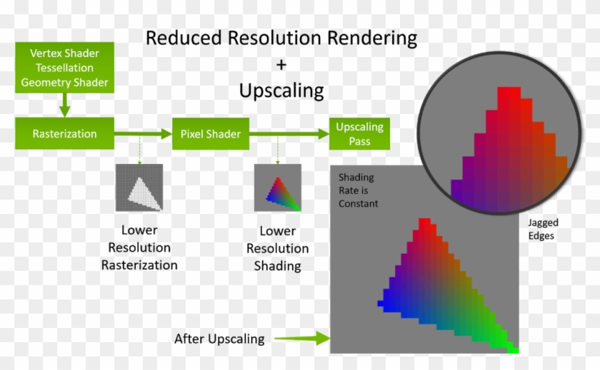
As far as I understand it, the screen can be divided into multiple subsections/zones, which can have a different pixel resolution.
Instead of processing for example 3840x2160 pixels (= 8,294,400 pixels), some subsections can use half-resolution or less, in the end you might effectively calculate ~5 million pixels, instead of ~8.
The final image obviously still consists of 3840x2160 pixels, but the screen zones with a lower resolution are upscaled appropriately to the final output.
Such a feature was also already supported by the PS4 Pro (and Polaris/GCN Gen4 GPUs), where the target application was the same as described by the patent, for VR rendering, where the center of the image is rasterized at full resolution and edges and corners with a lower resolution.
Draw-backs of such methods can be the complexity, as you need to carefuly handle zone transitions.
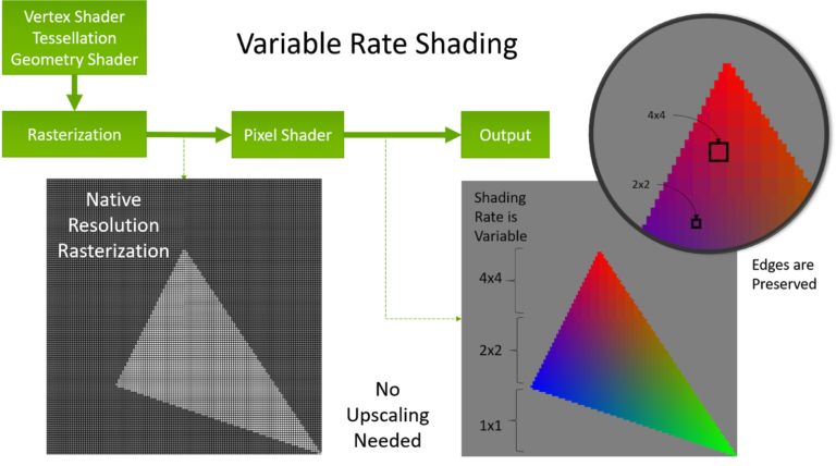
Another is that rasterization and pixel shading rate is coupled, the zones with a lower raster/pixel-resolution will also display geometry edges worse.
Here are two examples given by Apple and their Variable Rasterization Rate feature:
Without Variable Rate Shading
With Variable Rate Shading
Images via:
https://github.com/gpuweb/gpuweb/issues/450
VRS, as defined under DX12/Vulkan, decouples the pixel shading rate from the rasterization rate.
For example, the whole image/screen space is uniformly rasterized at the same resolution, but the pixel shading rate can be varied for the surface:
https://developer.nvidia.com/blog/turing-variable-rate-shading-vrworks/
Coupled with the fine control granularity, it's possible to use VRS for all kinds of applications fields.
Since Sony will again sell VR-Units, the PS5 may include some customizations to increase the efficiency of rendering to different viewports, but truly VRS equivalent functionality for many use cases most likely can't be replicated.
[2] INT4/INT8 dot-products are missing on two RDNA"1" parts, Navi10 and GFX1013.
Either that feature was not finished yet or there was a deliberate decision against the inclusion, I rather think it was the first option.
Microsoft may have started to work at a later point in time with AMD, than Sony, when some features were basically or already ready from the start.
Loxus
Member
Now that you detailed VRS.[1] All of those patent descriptions logically start with geometry assembly and then go over the rasterization process of that geometry, which also involves the pixel pipeline with Scan Converters, Pixel Shaders and ROPs.
AFAIK, this is one of the patents in question:
https://patents.google.com/patent/US9710881B2/en
Skimming over it, the concept appears to be similar to what is described as Multi-Resolution Shading, Variable Rasterization Rate or *Variable Rate Shading* by different companies and the respective marketing material.
The motivation behind it overlaps with some goals of VRS as specified under DX12, saving processing costs of Pixel Shaders, though there are some crucial differences.
As far as I understand it, the screen can be divided into multiple subsections/zones, which can have a different pixel resolution.
Instead of processing for example 3840x2160 pixels (= 8,294,400 pixels), some subsections can use half-resolution or less, in the end you might effectively calculate ~5 million pixels, instead of ~8.
The final image obviously still consists of 3840x2160 pixels, but the screen zones with a lower resolution are upscaled appropriately to the final output.
Such a feature was also already supported by the PS4 Pro (and Polaris/GCN Gen4 GPUs), where the target application was the same as described by the patent, for VR rendering, where the center of the image is rasterized at full resolution and edges and corners with a lower resolution.
Draw-backs of such methods can be the complexity, as you need to carefuly handle zone transitions.
Another is that rasterization and pixel shading rate is coupled, the zones with a lower raster/pixel-resolution will also display geometry edges worse.
Here are two examples given by Apple and their Variable Rasterization Rate feature:
Without Variable Rate Shading
With Variable Rate Shading
Images via:
https://github.com/gpuweb/gpuweb/issues/450
VRS, as defined under DX12/Vulkan, decouples the pixel shading rate from the rasterization rate.
For example, the whole image/screen space is uniformly rasterized at the same resolution, but the pixel shading rate can be varied for the surface:
https://developer.nvidia.com/blog/turing-variable-rate-shading-vrworks/
Coupled with the fine control granularity, it's possible to use VRS for all kinds of applications fields.
Since Sony will again sell VR-Units, the PS5 may include some customizations to increase the efficiency of rendering to different viewports, but truly VRS equivalent functionality for many use cases most likely can't be replicated.
[2] INT4/INT8 dot-products are missing on two RDNA"1" parts, Navi10 and GFX1013.
Either that feature was not finished yet or there was a deliberate decision against the inclusion, I rather think it was the first option.
Microsoft may have started to work at a later point in time with AMD, than Sony, when some features were basically or already ready from the start.
Do you know what GPU part Nvidia uses for VRS? We know AMD uses ROPs. Nvidia doesn't appear to have a patent on it.
And does Intel support VRS via dedicated hardware?
I haven't been really following up on Intel's new GPU in that regard.
I don't think you mentioned Intels VRS capabilities in your latest video. I may have to watch it again.
Last edited:
Yes - I was referencing that they discuss a bunch of different approaches and eventually settle on (ab)using the primitive assembly to assign different rasterization parameters to each zone. But that's too much text to extract from the patent right now[1] All of those patent descriptions logically start with geometry assembly and then go over the rasterization process of that geometry, which also involves the pixel pipeline with Scan Converters, Pixel Shaders and ROPs.
")
Not entirely - also to your earlier comment.Another is that rasterization and pixel shading rate is coupled, the zones with a lower raster/pixel-resolution will also display geometry edges worse.
Yes - but pixel-res is a subset of functionality, better explained in the updated patent:As far as I understand it, the screen can be divided into multiple subsections/zones, which can have a different pixel resolution.
EP3872767A1 - Method for efficient re-rendering objects to vary viewports and under varying rendering and rasterization parameters - Google Patents
Graphics processing renders a scene with a plurality of different rendering parameters for different locations on a screen area. A rendering parameter context is set up for each of a plurality of zones and each zone is assigned an index. An object covering at least two zones of the screen area...
patents.google.com


Note that each zone comes with an index looking up a full set of its own rasterization parameters(not just pixel res), so it does indeed allow changing individual parameters per-zone - but perhaps more importantly it also allows changing a bunch of other things - eg. you can even vary things like pixel/depth formats from one zone to the next, in addition to raster and shader rates (ie. it's a functional superset of everything we've seen to date in this space).
The real potential trade-off here IMO is the question of granularity - Pro's implementation was substantially more coarse than VRS in modern GPUs, but then we didn't need the granularity back then. With the intended use-cases here spanning eye-tracked FOV adjustments, one would expect a substantial increase in granularity in PS5 for it to be useful, but that's the part we don't have any official answer for yet.
I'd also mention that the trade-off you mention is two way. Being restricted to only sample-count variation in VRS breaks down any potential gains in high-geometry density areas, so to be able to really efficiently optimize we need access to other viewport parameters, starting with pixel density. This is especially important to applications like VR where pixel-edge quality dominates well ahead of shading quality, but it also opens up a ton of other potential for optimizing IQ (not just down, even for improving things, eg. selective supersampling etc).
ethomaz
Banned
VRS is different for each vendor even if standardized in DX12 each vendor has it own in hardware implementation.
That means that even the end resulting being similar (what are defined in DX12) how it works internally in the GPU is different for nVidia implementation and AMD implementation for example.
BTW nVidia VRS implementation is way before DX12 standardized it… nVidia didn't change it to adapt to DX12.
That means that even the end resulting being similar (what are defined in DX12) how it works internally in the GPU is different for nVidia implementation and AMD implementation for example.
BTW nVidia VRS implementation is way before DX12 standardized it… nVidia didn't change it to adapt to DX12.
Last edited:
ToTTenTranz
Banned
Even if we assume - for argument's sake - that GFX1013 = Cyan Skillfish = final PS5 hardware, you are assuming the GFX ID takes precedence in determining the featureset over the chronology of features that were incrementally introduced to RDNA GPUs.It looks exactly like Cyan Skillfish, because Cyan Skillfish = GFX1013
There are a couple of new instructions behind GFX10-3insts which are not supported by GFX1013.
It's not a community test repository, it's the LLVM compiler repository for AMD's GPUs.
The people contributing to it are official AMD employees, if they don't know what this GPU is, I don't know who will.
I'm not sure that is the case.
From what I see, the chronology of RDNA changes are as follows:
Mid-2019: First-gen RDNA1 (Navi 10) = baseline
Late 2019: Second-gen RDNA1 (Navi 12/14) = 1st gen RDNA1 + Dot4 INT8 / Dot8 INT4 for ML inference.
Late 2020: RDNA2 = 2nd gen RDNA1 + raytracing + sampler feedback + VRS2 + optimized clock/power curve + Infinity Cache + RBplus + others.
The PS5 GPU has raytracing and a clock/power curve similar to the RDNA2 dGPUs from late 2020.
I get how Sony could choose to keep the older RB units from RDNA1. The RDNA2 RB+ is more area optimized and brings support for VRS2, but using 4 RB per shader array total gives the PS5 twice the depth and stencil units. PC games don't seem to show an advantage for this, but Sony's 1st-party devs could have asked for this spec.
Also, considering the sheer number of patents Sony filed on foveated rendering and VRS, they definitely put a lot of thought into it. It could be that they're not interested in VRS2 because they prefer a pure compute solution that is more flexible and that they can better adapt for VR.
What I won't agree with is the assumption that it doesn't have Dot4 INT8 for ML inference.
Locuza
Member
| Answer Part 1: Again a posting error when all text is included |
In detail they are probably many smaller and larger differences between the rasterization pipelines from the three different vendors, but on a high-level view they follow a common picture.
VRS affects the color and depth pipeline and as such some hardware blocks have to be modified to support the new functionality, so it makes sense to enhance the units which already execute functions closely related to that task.
I would assume every vendor made adjustments to their Render Backend and potentially some other hardware blocks inside the whole raster pipeline.
Intel does support VRS Tier 1 under DX12 starting with Gen11 iGPUs (Ice Lake).
Xe LP (Tiger Lake, Rocket Lake, DG1) still only supports VRS Tier 1.
The upcoming Xe HPG GPUs from Intel (DG2) will support VRS Tier 2 and in general DX12 Ultimate (FL12_2).
I believe I did not explicitly mentioned it in the latest video.
A small anecdote.
There was a team at Intel exploring that concept half a decade ago, in 2014 they called it Coarse Pixel Shading (CPS):
https://fileadmin.cs.lth.se/graphics/research/papers/2014/cps/cps.pdf
According to David Kanter from the Linley Group, the bureaucratic product-development process and the 10nm delays at Intel led to the very late introduction with Ice Lake in 2019.
Nvidia's Turing architecture in 2018 was the first desktop line-up to provide that functionality, being also more advanced than on Ice Lake.
The funny part about it, it is claimed that most of the CPS team which previously worked with or at Intel was hired by Nvidia, effectively beating their previous work in terms of feature set and time-to-market.
https://www.linleygroup.com/mpr/article.php?id=12091
Of course IHVs work together with Microsoft and other standard bodies, everyone can propose features and some get standardized.
Many of the features found in DX are a direct result of the hw capabilities of the vendors (even for products which are not released yet), exposing their limits and functionalities.
Somewhere the patent said a zone can be a single pixel or larger, though for efficiency reasons you likely don't want to have too many zones.
I only read general statements about changing the pixel or sampling rate, which does not necessarily mean that the shading rate can work in a coarse manner like with VRS.
It may simply be the option to run a pixel shader invocation once per pixel or per sample count within a pixel, like using MSAA with x samples, but not necessarily that you can use one pixel shader for multiple pixels.
In regard to variable rasterization rate it would be also great to know which hardware capabilities "vanilla" RDNA1&2 offer from AMD, currently I don' think it's possible to extract anything concrete from the patent.
Now that you detailed VRS.
Do you know what GPU part Nvidia uses for VRS? We know AMD uses ROPs. Nvidia doesn't appear to have a patent on it.
And does Intel support VRS via dedicated hardware?
I haven't been really following up on Intel's new GPU in that regard.
I don't think you mentioned Intels VRS capabilities in your latest video. I may have to watch it again.
VRS is different for each vendor even if standardized in DX12 each vendor has it own in hardware implementation.
That means that even the end resulting being similar (what are defined in DX12) how it works internally in the GPU is different for nVidia implementation and AMD implementation for example.
BTW nVidia VRS implementation is way before DX12 standardized it… nVidia didn't change it to adapt to DX12.
In detail they are probably many smaller and larger differences between the rasterization pipelines from the three different vendors, but on a high-level view they follow a common picture.
VRS affects the color and depth pipeline and as such some hardware blocks have to be modified to support the new functionality, so it makes sense to enhance the units which already execute functions closely related to that task.
I would assume every vendor made adjustments to their Render Backend and potentially some other hardware blocks inside the whole raster pipeline.
Intel does support VRS Tier 1 under DX12 starting with Gen11 iGPUs (Ice Lake).
Xe LP (Tiger Lake, Rocket Lake, DG1) still only supports VRS Tier 1.
The upcoming Xe HPG GPUs from Intel (DG2) will support VRS Tier 2 and in general DX12 Ultimate (FL12_2).
I believe I did not explicitly mentioned it in the latest video.
A small anecdote.
There was a team at Intel exploring that concept half a decade ago, in 2014 they called it Coarse Pixel Shading (CPS):
https://fileadmin.cs.lth.se/graphics/research/papers/2014/cps/cps.pdf
According to David Kanter from the Linley Group, the bureaucratic product-development process and the 10nm delays at Intel led to the very late introduction with Ice Lake in 2019.
Nvidia's Turing architecture in 2018 was the first desktop line-up to provide that functionality, being also more advanced than on Ice Lake.
The funny part about it, it is claimed that most of the CPS team which previously worked with or at Intel was hired by Nvidia, effectively beating their previous work in terms of feature set and time-to-market.
https://www.linleygroup.com/mpr/article.php?id=12091
Of course IHVs work together with Microsoft and other standard bodies, everyone can propose features and some get standardized.
Many of the features found in DX are a direct result of the hw capabilities of the vendors (even for products which are not released yet), exposing their limits and functionalities.
I went through the first 10 pages of that patent and decided I will not read the rest. x)Yes - I was referencing that they discuss a bunch of different approaches and eventually settle on (ab)using the primitive assembly to assign different rasterization parameters to each zone. But that's too much text to extract from the patent right now
Not entirely - also to your earlier comment.
Yes - but pixel-res is a subset of functionality, better explained in the updated patent:
[removed images]EP3872767A1 - Method for efficient re-rendering objects to vary viewports and under varying rendering and rasterization parameters - Google Patents
Graphics processing renders a scene with a plurality of different rendering parameters for different locations on a screen area. A rendering parameter context is set up for each of a plurality of zones and each zone is assigned an index. An object covering at least two zones of the screen area...patents.google.com
Note that each zone comes with an index looking up a full set of its own rasterization parameters(not just pixel res), so it does indeed allow changing individual parameters per-zone - but perhaps more importantly it also allows changing a bunch of other things - eg. you can even vary things like pixel/depth formats from one zone to the next, in addition to raster and shader rates (ie. it's a functional superset of everything we've seen to date in this space).
The real potential trade-off here IMO is the question of granularity - Pro's implementation was substantially more coarse than VRS in modern GPUs, but then we didn't need the granularity back then. With the intended use-cases here spanning eye-tracked FOV adjustments, one would expect a substantial increase in granularity in PS5 for it to be useful, but that's the part we don't have any official answer for yet.
I'd also mention that the trade-off you mention is two way. Being restricted to only sample-count variation in VRS breaks down any potential gains in high-geometry density areas, so to be able to really efficiently optimize we need access to other viewport parameters, starting with pixel density. This is especially important to applications like VR where pixel-edge quality dominates well ahead of shading quality, but it also opens up a ton of other potential for optimizing IQ (not just down, even for improving things, eg. selective supersampling etc).
Somewhere the patent said a zone can be a single pixel or larger, though for efficiency reasons you likely don't want to have too many zones.
I only read general statements about changing the pixel or sampling rate, which does not necessarily mean that the shading rate can work in a coarse manner like with VRS.
It may simply be the option to run a pixel shader invocation once per pixel or per sample count within a pixel, like using MSAA with x samples, but not necessarily that you can use one pixel shader for multiple pixels.
In regard to variable rasterization rate it would be also great to know which hardware capabilities "vanilla" RDNA1&2 offer from AMD, currently I don' think it's possible to extract anything concrete from the patent.
Last edited:
Locuza
Member
| Answer Part 2: Because a posting error would occur when all text was included |
For some that's not true, like there is stuff like gfx90a (Aldebaran/CDNA2) which has the Graphics Core Version 9.4.2.
Navi12 has the GFX Target 1011, Navi14 = GFX Target 1012, however Navi12 is actually the newer project, the Graphics Core Version for Navi12 is 10.1.2, while Navi14 is using the older 10.1.1 GC IP.
For Cyan Skillfish the GFX Target and IP version is using the same number series, the GFX Target is 1013 and the Graphics Core Version is stated to be 10.1.3.
It would indicate that the IP block development started after Navi12.
According to AMD's driver and compiler code, Cyan Skillfish supports Ray Tracing but not INT Dot4/Dot8.
So obviously there is an GPU which doesn't follow the chronological introduction of features from Navi10 to Navi12.
I think you have to agree that it's hard to explain Cyan Skillfish, without the PS5 SoC coming into mind.
Like if it's a new semi-custom design, why would AMD use old RDNA"1" IP blocks?
Why would AMD include Raytracing support, but not include DP4/8?
Why does this thing look exactly like the PS5 from a high-level view?
It has 8 Zen2-Cores, 256-Bit GDDR6 @14Gbps, the same GPU-Cache-Configuration as the PS5 and also 5 WGPs per Shader-Array.
For some reason the customer also only wanted 2 Display Controllers, as the PS5 SoC.
Thanks to the die shots we know that the PS5 has 2x Display PHYs, an SoC Floorplan which resembles Navi10 and uses the old Render Backend design.
And thanks to comments from id Tech in relation to their game Doom Eternal, we also know that HW VRS is not supported by the PS5.
Without id Tech's commentary there could have been a last straw of hope, like imaging that maybe the PS5 uses the old RB configuration but developed it further with the inclusion of VRS, but that's not the case.
I started to question if the PS5 supports VRS and DOT4/8, when Mark Cerny did not explicitly mentioned those fairly large bullet points in their YouTube video "Road to PS5" and when the tech reports with Digital Foundry also did not mentioned it.
After that I held the following position, alright let's wait for die shots and see if the ROPs are different and when the first multi-platform games come out with VRS.
Now many months later the situation is clear, old RB configuration and no VRS functionality as it's found on RDNA2 and Xbox Series hw.
In regard to the DOT4/8 support I did not have high hopes anymore and it was later mentioned by David Cage in an interview that it's one advantage of the Xbox Series in comparison to the PS5:
Since that point I was heavily leaning towards the idea, that DP4/8 is also missing.
With Cyan Skillfish a very coherent picture is presented and I think we have a very strong case here, that the PS5 lacks those capabilities.
Now, this doesn't mean that all RDNA"1" IP blocks have the same design implementation.
The PS5 obviously clocks way higher than RDNA"1" GPUs like Navi10, 14 and 12 and it presents a much better energy efficiency.
So definietly some or rather most of the design work of RDNA2 was also used for the PS5 console.
Personally I stated that I consider the whole package as important, better energy efficiency and way higher clock rates are one of the largest achievements of AMD's RDNA2 work.
Ray Tracing acceleration is a very specific, but huge performance booster and part of the PS5 HW.
And of course customizations like Cache Scrubbers, which are exclusive to Sony and not found on Xbox Series nor PC RDNA2 GPUs, don't fit into RDNA1 and RDNA2 comparisons, since they live outside of it.
Personally I classify the PS5 and Xbox Series simply as custom RDNA GPUs and that's it.
Claiming that the PS5/Xbox Series tech is RDNA1 or RDNA2 may lead to the wrong impression, since reality is (far) more nuanced than that.
For many, but not all GPUs, the GFX ID is aligned with the Graphics Core IP Version.Even if we assume - for argument's sake - that GFX1013 = Cyan Skillfish = final PS5 hardware, you are assuming the GFX ID takes precedence in determining the featureset over the chronology of features that were incrementally introduced to RDNA GPUs.
I'm not sure that is the case.
From what I see, the chronology of RDNA changes are as follows:
Mid-2019: First-gen RDNA1 (Navi 10) = baseline
Late 2019: Second-gen RDNA1 (Navi 12/14) = 1st gen RDNA1 + Dot4 INT8 / Dot8 INT4 for ML inference.
Late 2020: RDNA2 = 2nd gen RDNA1 + raytracing + sampler feedback + VRS2 + optimized clock/power curve + Infinity Cache + RBplus + others.
The PS5 GPU has raytracing and a clock/power curve similar to the RDNA2 dGPUs from late 2020.
I get how Sony could choose to keep the older RB units from RDNA1. The RDNA2 RB+ is more area optimized and brings support for VRS2, but using 4 RB per shader array total gives the PS5 twice the depth and stencil units. PC games don't seem to show an advantage for this, but Sony's 1st-party devs could have asked for this spec.
Also, considering the sheer number of patents Sony filed on foveated rendering and VRS, they definitely put a lot of thought into it. It could be that they're not interested in VRS2 because they prefer a pure compute solution that is more flexible and that they can better adapt for VR.
What I won't agree with is the assumption that it doesn't have Dot4 INT8 for ML inference.
For some that's not true, like there is stuff like gfx90a (Aldebaran/CDNA2) which has the Graphics Core Version 9.4.2.
Navi12 has the GFX Target 1011, Navi14 = GFX Target 1012, however Navi12 is actually the newer project, the Graphics Core Version for Navi12 is 10.1.2, while Navi14 is using the older 10.1.1 GC IP.
For Cyan Skillfish the GFX Target and IP version is using the same number series, the GFX Target is 1013 and the Graphics Core Version is stated to be 10.1.3.
It would indicate that the IP block development started after Navi12.
According to AMD's driver and compiler code, Cyan Skillfish supports Ray Tracing but not INT Dot4/Dot8.
So obviously there is an GPU which doesn't follow the chronological introduction of features from Navi10 to Navi12.
I think you have to agree that it's hard to explain Cyan Skillfish, without the PS5 SoC coming into mind.
Like if it's a new semi-custom design, why would AMD use old RDNA"1" IP blocks?
Why would AMD include Raytracing support, but not include DP4/8?
Why does this thing look exactly like the PS5 from a high-level view?
It has 8 Zen2-Cores, 256-Bit GDDR6 @14Gbps, the same GPU-Cache-Configuration as the PS5 and also 5 WGPs per Shader-Array.
For some reason the customer also only wanted 2 Display Controllers, as the PS5 SoC.
Thanks to the die shots we know that the PS5 has 2x Display PHYs, an SoC Floorplan which resembles Navi10 and uses the old Render Backend design.
And thanks to comments from id Tech in relation to their game Doom Eternal, we also know that HW VRS is not supported by the PS5.
Without id Tech's commentary there could have been a last straw of hope, like imaging that maybe the PS5 uses the old RB configuration but developed it further with the inclusion of VRS, but that's not the case.
I started to question if the PS5 supports VRS and DOT4/8, when Mark Cerny did not explicitly mentioned those fairly large bullet points in their YouTube video "Road to PS5" and when the tech reports with Digital Foundry also did not mentioned it.
After that I held the following position, alright let's wait for die shots and see if the ROPs are different and when the first multi-platform games come out with VRS.
Now many months later the situation is clear, old RB configuration and no VRS functionality as it's found on RDNA2 and Xbox Series hw.
In regard to the DOT4/8 support I did not have high hopes anymore and it was later mentioned by David Cage in an interview that it's one advantage of the Xbox Series in comparison to the PS5:
https://wccftech.com/xbox-series-xs...ning-powered-shader-cores-says-quantic-dream/David Cage: The shader cores of the Xbox are also more suitable to machine learning, which could be an advantage if Microsoft succeeds in implementing an equivalent to Nvidia's DLSS (an advanced neural network solution for AI).
Since that point I was heavily leaning towards the idea, that DP4/8 is also missing.
With Cyan Skillfish a very coherent picture is presented and I think we have a very strong case here, that the PS5 lacks those capabilities.
Now, this doesn't mean that all RDNA"1" IP blocks have the same design implementation.
The PS5 obviously clocks way higher than RDNA"1" GPUs like Navi10, 14 and 12 and it presents a much better energy efficiency.
So definietly some or rather most of the design work of RDNA2 was also used for the PS5 console.
Personally I stated that I consider the whole package as important, better energy efficiency and way higher clock rates are one of the largest achievements of AMD's RDNA2 work.
Ray Tracing acceleration is a very specific, but huge performance booster and part of the PS5 HW.
And of course customizations like Cache Scrubbers, which are exclusive to Sony and not found on Xbox Series nor PC RDNA2 GPUs, don't fit into RDNA1 and RDNA2 comparisons, since they live outside of it.
Personally I classify the PS5 and Xbox Series simply as custom RDNA GPUs and that's it.
Claiming that the PS5/Xbox Series tech is RDNA1 or RDNA2 may lead to the wrong impression, since reality is (far) more nuanced than that.
Depth @ 1, Raster @ 1/4, MSAAx4 = 4 pixels receive one shader sample (ie. VRS 2x2). You can do other sample arrangements as well - obviously.It may simply be the option to run a pixel shader invocation once per pixel or per sample count within a pixel, like using MSAA with x samples, but not necessarily that you can use one pixel shader for multiple pixels.
Yea, which is why I said granularity is the big question. There is mentions of suggested region-sizes in 32x32 - 64x64 range I've seen elsewhere, but we have nothing to go by yet in terms of what an actual implementation might be (as mentioned, Pro was much coarser than that).Somewhere the patent said a zone can be a single pixel or larger, though for efficiency reasons you likely don't want to have too many zones.
thanks I exactly think the same| Answer Part 2: Because a posting error would occur when all text was included |
For many, but not all GPUs, the GFX ID is aligned with the Graphics Core IP Version.
For some that's not true, like there is stuff like gfx90a (Aldebaran/CDNA2) which has the Graphics Core Version 9.4.2.
Navi12 has the GFX Target 1011, Navi14 = GFX Target 1012, however Navi12 is actually the newer project, the Graphics Core Version for Navi12 is 10.1.2, while Navi14 is using the older 10.1.1 GC IP.
For Cyan Skillfish the GFX Target and IP version is using the same number series, the GFX Target is 1013 and the Graphics Core Version is stated to be 10.1.3.
It would indicate that the IP block development started after Navi12.
According to AMD's driver and compiler code, Cyan Skillfish supports Ray Tracing but not INT Dot4/Dot8.
So obviously there is an GPU which doesn't follow the chronological introduction of features from Navi10 to Navi12.
I think you have to agree that it's hard to explain Cyan Skillfish, without the PS5 SoC coming into mind.
Like if it's a new semi-custom design, why would AMD use old RDNA"1" IP blocks?
Why would AMD include Raytracing support, but not include DP4/8?
Why does this thing look exactly like the PS5 from a high-level view?
It has 8 Zen2-Cores, 256-Bit GDDR6 @14Gbps, the same GPU-Cache-Configuration as the PS5 and also 5 WGPs per Shader-Array.
For some reason the customer also only wanted 2 Display Controllers, as the PS5 SoC.
Thanks to the die shots we know that the PS5 has 2x Display PHYs, an SoC Floorplan which resembles Navi10 and uses the old Render Backend design.
And thanks to comments from id Tech in relation to their game Doom Eternal, we also know that HW VRS is not supported by the PS5.
Without id Tech's commentary there could have been a last straw of hope, like imaging that maybe the PS5 uses the old RB configuration but developed it further with the inclusion of VRS, but that's not the case.
I started to question if the PS5 supports VRS and DOT4/8, when Mark Cerny did not explicitly mentioned those fairly large bullet points in their YouTube video "Road to PS5" and when the tech reports with Digital Foundry also did not mentioned it.
After that I held the following position, alright let's wait for die shots and see if the ROPs are different and when the first multi-platform games come out with VRS.
Now many months later the situation is clear, old RB configuration and no VRS functionality as it's found on RDNA2 and Xbox Series hw.
In regard to the DOT4/8 support I did not have high hopes anymore and it was later mentioned by David Cage in an interview that it's one advantage of the Xbox Series in comparison to the PS5:
https://wccftech.com/xbox-series-xs...ning-powered-shader-cores-says-quantic-dream/
Since that point I was heavily leaning towards the idea, that DP4/8 is also missing.
With Cyan Skillfish a very coherent picture is presented and I think we have a very strong case here, that the PS5 lacks those capabilities.
Now, this doesn't mean that all RDNA"1" IP blocks have the same design implementation.
The PS5 obviously clocks way higher than RDNA"1" GPUs like Navi10, 14 and 12 and it presents a much better energy efficiency.
So definietly some or rather most of the design work of RDNA2 was also used for the PS5 console.
Personally I stated that I consider the whole package as important, better energy efficiency and way higher clock rates are one of the largest achievements of AMD's RDNA2 work.
Ray Tracing acceleration is a very specific, but huge performance booster and part of the PS5 HW.
And of course customizations like Cache Scrubbers, which are exclusive to Sony and not found on Xbox Series nor PC RDNA2 GPUs, don't fit into RDNA1 and RDNA2 comparisons, since they live outside of it.
Personally I classify the PS5 and Xbox Series simply as custom RDNA GPUs and that's it.
Claiming that the PS5/Xbox Series tech is RDNA1 or RDNA2 may lead to the wrong impression, since reality is (far) more nuanced than that.
assurdum
Banned
They are not cut. Sony has designed the GPU from the ground and it was intended to be like this intentionally. If AMD has updated RDNA2 later with more features, probably Sony taken in the count to prefer their own solutions to what AMD would have offered to them later. Neither XSX is full RDNA2 in many aspects. Is it MS came out to say to the people infinite cache was absent on XSX hardware or they have avoid smartly the argument and let the people find out later scanned physically the SOC?Sony has marketed the PS5 GPU as an RDNA 2.0 GPU. If it is lacking RDNA 2.0 features that means those features were cut.
If they never intended those features to be in the PS5 then just come out and say hey we dont support them. I dont understand why after being so open about the tech in the PS4 and PS4 Pro they have gone dead silent after the Road to PS5 hiding Mark Cerny is a dungeon for over a year.
Last edited: