-
Hey, guest user. Hope you're enjoying NeoGAF! Have you considered registering for an account? Come join us and add your take to the daily discourse.
You are using an out of date browser. It may not display this or other websites correctly.
You should upgrade or use an alternative browser.
You should upgrade or use an alternative browser.
AMD Radeon 300 series (possible) specs
- Thread starter wachie
- Start date
No, probably not.Is there any chance of a 390x variation with more ram? Even a custom one by Sapphire, Asus and so on? Because 4GB isn't looking great, even with HBM. Everything else looks great, though.
No, probably not.
Hmm. Not sure what to do, now. I guess I'll wait for real-world benchmarks to come rolling in.
Is there any chance of a 390x variation with more ram? Even a custom one by Sapphire, Asus and so on? Because 4GB isn't looking great, even with HBM. Everything else looks great, though.
Probably only when the 4xx series arrives, if they manage to successfully transition to HBM 2
The leak for water cooled IHS was far more reliable. And most likely its going to be on 28nm and that >500mm chip so I'm not expecting it to be a lean GPU.The linkedin profile mentioned 300w TDP. But as we all know TDP is not actual power consumption.
A 290x at stock didn't consume 290w and neither did some overclocked models :
http://www.techpowerup.com/reviews/Sapphire/R9_290X_Tri-X_OC/22.html
opticalmace
Member
Is there any chance of a 390x variation with more ram? Even a custom one by Sapphire, Asus and so on? Because 4GB isn't looking great, even with HBM. Everything else looks great, though.
There was an 8GB 290x... I wouldn't say it's out of the question.
To be frank, I'm not too impressed by Tonga's compression algorithms. Either the card is really unbalanced or something else is up.
The fact Tonga is faster at pixel fillrate than a 290X despite having a lot less bandwidth and half the number of ROPs just shows how great the compression algorithms are.
The fact is the card is pretty much a 7950 with less memory bandwidth and less VRAM yet it performs faster.
lukeskymac
Member
If this is the case how come the PS4 got 8GB and why couldn't they use that technology for a graphics card? Also isn't there a 6GB graphics card already out by Nvidia?
Uh... because PS4 uses GDDR5 instead of HBM?
Is there a technical limitation to HBM to that or just manufacturing availability?No, probably not.
PC GPUs don't exist to provide any kind of proof of future performance. The entire premise is flawed. These devices are superseded at their price point 18-24 months following release. Sometimes sooner. There is no future proofing. There is only, 'what I am willing to spend'.
It's simply at total odds with the realities of semi-conductor development and especially that of the GPU, the performance of which scales almost linearly with transistor count.
In the case of the design in question, there has to be a HBM1 design so they can sell some units and make money to cover the R&D costs. There'll be an HBM2 design later on that can support higher densities. The HBM1 process was only very recently finalised I think.
It's not a huge mistake because the product will certainly out-perform their existing design by a considerable margin and not everyone owns a 290x or 970 already.
I realize that future proofing is a silly concept, but like I said in light of the 970 debacle people have been going nuts about it. And it's only not a huge mistake if the next Nvidia cards stop at 4gb as well. If they come out in 6-8-12gb versions AMD will look really bad when people start showing benchmarks using >4gb of vram. HBM looks pretty amazing, but it doesn't change what happens when the vram fills up and a card chokes.
Higher bandwidth, should certain games be bandwidth-limited.What will HBM offer? Better performance at higher resolutions?
I'm honestly not sure if 2015/2016 games will hit BW-limited scenarios before GPU horsepower.
Their theme is islands with volcanoes. Bad choice since teamgreen is having a field day with TDP jokes <.<Heh, I lived in Grenada for a while...not exactly a place I associate with high speed
maneil99
Member
Higher bandwidth, should certain games be bandwidth-limited.
I'm honestly not sure if 2015/2016 games will hit BW-limited scenarios before GPU horsepower.
I suppose with higher res textures and higher resolution alpha effects it could come in the place alot sooner but current GPUS have alot of headroom and normally simply hit a VRAM limit vs BW so yeah
Reallink
Member
PC GPUs don't exist to provide any kind of proof of future performance. The entire premise is flawed. These devices are superseded at their price point 18-24 months following release. Sometimes sooner. There is no future proofing. There is only, 'what I am willing to spend'.
It's simply at total odds with the realities of semi-conductor development and especially that of the GPU, the performance of which scales almost linearly with transistor count.
Future proof refers to far more than maxing games, not really sure where that notion comes from. No one with half an ounce of sense expects a card to Ultra games for 3 years, an entire generation, or whatever arbitrary goals you're imagining. If you want to limit it to the extremes, at the basest level, the concept is really defined as "can I run new games period in X-number of years". For a specific example, the 5 year old 768MB GTX 460 probably can not run modern games at all, and hasn't been able to for quite a while, so clearly it was a very poor choice in terms of future proofing. On the other hand a 1GB+ GTX 460/470/480 from the same time probably can, likely well beyond acceptable levels in the higher tiers/OC's, so you might say those were very future proof cards. Again, this is just limiting it to extremes, obviously there are situations everywhere in between where you might consider one card future proof and another not. Say 3 years from now you have to use Med/Low textures on your new favorite game while that other card you were considering at the time can still do High or Ultra. That is what people mean by future proof, not zomg you mean I can't uber sample Witcher 4 on my 980.
What? Can you please share where you saw this?The fact Tonga is faster at pixel fillrate than a 290X despite having a lot less bandwidth and half the number of ROPs just shows how great the compression algorithms are.
The fact is the card is pretty much a 7950 with less memory bandwidth and less VRAM yet it performs faster.
Mad Season
Banned
Coming from a 7950. Should I wait for this or get a 980? I'm leaning nvidia...
Waiting a couple of months wont hurt, hell even might catch a few price cuts on the 980.Coming from a 7950. Should I wait for this or get a 980? I'm leaning nvidia...
Mad Season
Banned
Due out in April?Waiting a couple of months wont hurt, hell even might catch a few price cuts on the 980.
jfoul
Member
Is there a technical limitation to HBM to that or just manufacturing availability?
I think it's the spec of first gen HBM.
Mr_Antimatter
Member
Have you seen the insides of a ps4?
There are 16 memory chips around the SoC.
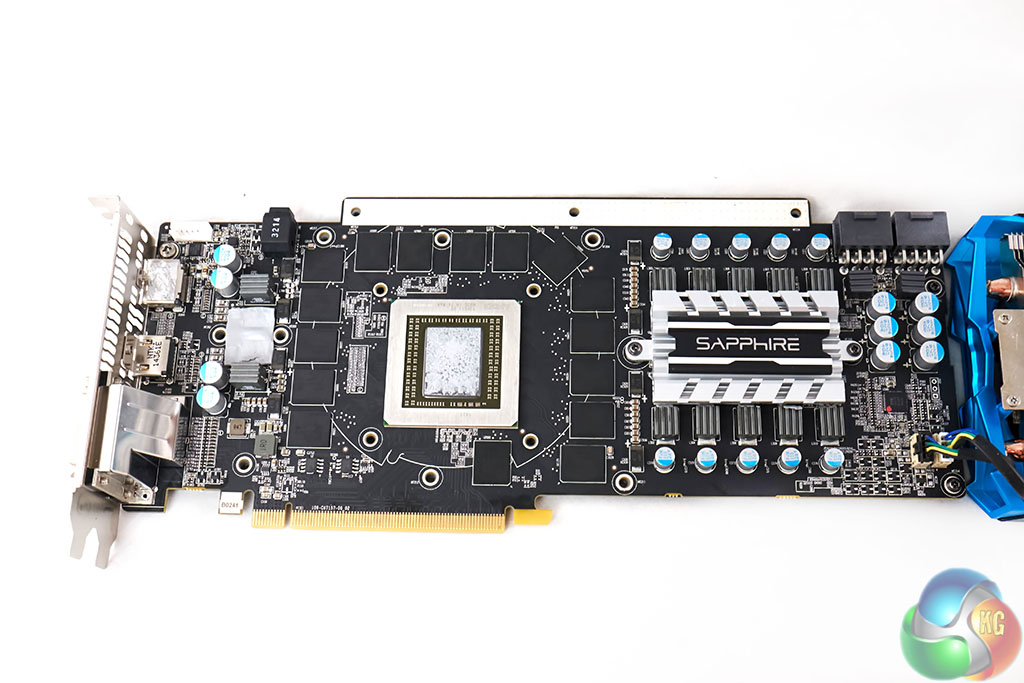
I still look at that motherboard and think it's pretty damn spiffy a design.
Someone please correct me on this if I'm wrong, but I think its a *mainly* technical limitations at the moment. They can only do a 4-high stack. And I'm going out on a limb here and guessing that since the largest single RAM size we have now is 1GB, that it means a 4GB limitation? We need 8 high stacks(or more) and/or larger single RAM sizes to get increases.Is there a technical limitation to HBM to that or just manufacturing availability?
Pimpbaa
Member
I still look at that motherboard and think it's pretty damn spiffy a design.
Especially compared to the xb1 motherboard. Dunno why the ps4 looks so much cleaner.
I can understand the disappointment at 4GB, but hopefully most of you weren't expecting much more for a brand new technology.
The biggest worry I have is that much higher BW is really valuable when you have more memory - 4GB will be nice for AA but it seems like the 4Gb version would be relatively unbalanced - too much bandwidth for the amount of ram.
The biggest worry I have is that much higher BW is really valuable when you have more memory - 4GB will be nice for AA but it seems like the 4Gb version would be relatively unbalanced - too much bandwidth for the amount of ram.
Ya I'm thinking it's the only available stack size from Hynix, not because of some architectural limit hopefully.Someone please correct me on this if I'm wrong, but I think its a *mainly* technical limitations at the moment. They can only do a 4-high stack. And I'm going out on a limb here and guessing that since the largest single RAM size we have now is 1GB, that it means a 4GB limitation? We need 8 high stacks(or more) and larger single RAM sizes to get increases.
If Hynix can volume the next stack, we can probably see 8GB cards.
Just read a bit more on it and it seems its not limited by RAM size, as they use 256MB slices to form each 1GB layer. So yes, stack size looks like the next thing to increase to get us to 8GB.
Man. 16nm 400-series with 8GB of super high bandwidth memory should be fucking monsters. At this point, I'm thinking I'm gonna stick with my 970 til then and skip this first round.
Man. 16nm 400-series with 8GB of super high bandwidth memory should be fucking monsters. At this point, I'm thinking I'm gonna stick with my 970 til then and skip this first round.
Just read a bit more on it and it seems its not limited by RAM size, as they use 256MB slices to form each 1GB layer. So yes, stack size looks like the next thing to increase to get us to 8GB.
Man. 16nm 400-series with 8GB of super high bandwidth memory should be fucking monsters. At this point, I'm thinking I'm gonna stick with my 970 til then and skip this first round.
And then VR-SLI, driving a 4k 2016 oculus Rift. Yum.
http://www.fudzilla.com/news/processors/36968-tmsc-to-invest-16-billion-in-advanced-chip-factory
Seems like 20nm GPU dream is dying/dead.
Seems like 20nm GPU dream is dying/dead.
Great time to be a PC gamer.And then VR-SLI, driving a 4k 2016 oculus Rift. Yum.
God damn the chip business is expensive.http://www.fudzilla.com/news/processors/36968-tmsc-to-invest-16-billion-in-advanced-chip-factory
Seems like 20nm GPU dream is dying/dead.
ashecitism
Member
There have been rumors/infos floating around for a while that both Nvidia and AMD will skip 20nm and go 16nm next year. That article doesn't come as a shocker. Though since AMD went to GloFo they'll go to 14nm?
maneil99
Member
Great time to be a PC gamer.
God damn the chip business is expensive.
Just give me the real maxwell
Why is 20nm difficult but 16 and even 10nm is possible? Is it the finFET bit? A change in process rather than just size?
But we are getting mobile chips in 20nm now so is that just a limitation of scale - you can't do really big power hungry chips at that size easily?
Your last sentence actually answers why it's so difficult, all those phone cpu and nand orders for 20nm chips is eating up all the capacity, which means no space for GPU orders.
Its not that the supply is being eaten up, its that the 20nm process, for whatever reason(that I couldn't tell you), isn't suited for desktop GPU architecture. I think it doesn't handle higher power or heat very reliably, making it too risky and inefficient to throw into mass GPU production. 14/16nm is supposedly more stable.Your last sentence actually answers why it's so difficult, all those phone cpu and nand orders for 20nm chips is eating up all the capacity, which means no space for GPU orders.
Its not that the supply is being eaten up, its that the 20nm process, for whatever reason(that I couldn't tell you), isn't suited for desktop GPU architecture. I think it doesn't handle higher power or heat very reliably, making it too risky and inefficient to throw into mass GPU production. 14/16nm is supposedly more stable.
Anandtech pointed out it's a situation of 3 options over 28nm pick 2:
30% faster
1.9x density
-25% less power draw
power and speed tend to be directly opposed though.
http://www.anandtech.com/show/8554/the-iphone-6-review/2
I'm not sure how that's different (historically) to dropping down to 28nm especially in power draw and speed being directly opposed options.
Anandtech also alludes that the trade offs are different when comparing Samsung's 20nm vs TSMC, which is sort of moot as I'm guessing Samsung's never really been interested in selling production to AMD/Nvidia when they need it for their SSD and own CPU's.
Also considering all the 20nm PowerVR GPU's being put in mobile devices what exactly is "problematic" with desktop GPU's at 20nm when it's fine with CPU's GPU's and SSD's in varying consumer products since 2014.
AMD also wants to give 20nm to Sony and Microsoft for their consoles (including the GPU obviously), why would 20nm become horrid only in desktop PC's GPU's? http://www.techpowerup.com/206857/amd-to-give-20-nm-optical-shrinks-to-console-socs-first.html
OminoMichelin
Member
Great time to be a PC gamer.
God damn the chip business is expensive.
Yea, I really want to see a paradigm shift soon-ish. Shame that most alternative technologies (graphene, nanotubes and so one) seem so far away.
Someone please correct me on this if I'm wrong, but I think its a *mainly* technical limitations at the moment. They can only do a 4-high stack. And I'm going out on a limb here and guessing that since the largest single RAM size we have now is 1GB, that it means a 4GB limitation? We need 8 high stacks(or more) and/or larger single RAM sizes to get increases.
Couldn't they just cram more chips on the card? Similar to the 16x512 MB in the 290X 8GB?
Anandtech pointed out it's a situation of 3 options over 28nm pick 2:
30% faster
1.9x density
-25% less power draw
power and speed tend to be directly opposed though.
http://www.anandtech.com/show/8554/the-iphone-6-review/2
I'm not sure how that's different (historically) to dropping down to 28nm especially in power draw and speed being directly opposed options.
Anandtech also alludes that the trade offs are different when comparing Samsung's 20nm vs TSMC, which is sort of moot as I'm guessing Samsung's never really been interested in selling production to AMD/Nvidia when they need it for their SSD and own CPU's.
Also considering all the 20nm PowerVR GPU's being put in mobile devices what exactly is "problematic" with desktop GPU's at 20nm when it's fine with CPU's GPU's and SSD's in varying consumer products since 2014.
AMD also wants to give 20nm to Sony and Microsoft for their consoles (including the GPU obviously), why would 20nm become horrid only in desktop PC's GPU's? http://www.techpowerup.com/206857/amd-to-give-20-nm-optical-shrinks-to-console-socs-first.html
The numbers you quote there are for 20nm LP (low power) devices. The benefits for High Power devices are just not there on TSMC's 20nm process (or GlobalFoundries' for that matter). TSMC's 20nm process does not use FinFET (which is going to be needed for it to be worthwhile for HP devices) and is named 20-SoC for a reason.
Also, you cannot point to NAND or other components as proof that 20nm works for the GPUs we're discussing. The products are too different. Intel are way ahead of everyone and they needed FinFET to get the benefits for their HP CPUs on their 22nm process and they're using FinFET again on their 14nm process.
Expect High Power GPUs to skip the 20nm processes available from TSMC and GlobalFoundries and instead move to 16nm with FinFET. It's more suitable for these High Power products.
These cards are using stacked memory now. Its entirely new technology and doesn't work like before. There wont be 8 or 16 memory modules scattered about as they are layered on top of each other now.Couldn't they just cram more chips on the card? Similar to the 16x512 MB in the 290X 8GB?
Expect High Power GPUs to skip the 20nm processes available from TSMC and GlobalFoundries and instead move to 16nm with FinFET. It's more suitable for these High Power products.
I'm adding a bit here, but I remember reading that 16FF is basically a 20nm process with FinFets. 16FF+ will supposedly actually be 16nm with FinFets (for TSMC). It just shows that a lot marketing fluff goes on with chip foundries too. The whole Xnm doesn't even say much anymore nowadays as all processes have different characteristics and sizes. At least, that's what I make out of it with my limited knowledge.
I wonder if there was any truth to the rumors saying that AMD was switching back to GF for their GPUs. Supposedly their 28nm HP (whatever it was called) is slightly better.
Objectively Bad Opinion
Member
These cards are using stacked memory now. Its entirely new technology and doesn't work like before. There wont be 8 or 16 memory modules scattered about as they are layered on top of each other now.
It will look like those mockups Nvidia showed for Volta/Pascal, except on a regular add-in board form factor.
Currently the 20nm process is planar instead of FinFET, so unlikely there will be confusion there I think.I'm adding a bit here, but I remember reading that 16FF is basically a 20nm process with FinFets. 16FF+ will supposedly actually be 16nm with FinFets (for TSMC). It just shows that a lot marketing fluff goes on with chip foundries too.
I'm adding a bit here, but I remember reading that 16FF is basically a 20nm process with FinFets. 16FF+ will supposedly actually be 16nm with FinFets (for TSMC). It just shows that a lot marketing fluff goes on with chip foundries too. The whole Xnm doesn't even say much anymore nowadays as all processes have different characteristics and sizes. At least, that's what I make out of it with my limited knowledge.
I wonder if there was any truth to the rumors saying that AMD was switching back to GF for their GPUs. Supposedly their 28nm HP (whatever it was called) is slightly better.
Yes, this is true about marketing. I think GlobalFoundries are even calling their next process 14nm + FinFET. As you say, there's a lot of complexity now and so relying on this simple nm moniker alone is not going to give you enough information.
Currently the 20nm process is planar instead of FinFET, so unlikely there will be confusion there I think.
Oh no, I meant there is 20nm planar (the one currently being used for low power devices), 16FF (which is still at 20nm size with FinFet but renamed to 16 instead) and 16FF+. I remember seeing a slide somewhere about it, but I can't seem to find it anymore. It doesn't really matter, I was just pointing out.
Its not that the supply is being eaten up, its that the 20nm process, for whatever reason(that I couldn't tell you), isn't suited for desktop GPU architecture. I think it doesn't handle higher power or heat very reliably, making it too risky and inefficient to throw into mass GPU production. 14/16nm is supposedly more stable.
That is 20nm on non intel is giving poor yields because it is a non finfet process. Intel managed to produce 22nm because it was already a finfet process (and I also suspect that Intel can eat some yield margins that others cannot).
The only available process node that is reliable is LPM like, which means only low power SoCs need apply.