Only thing they care about is that they have 8GB coherent memory with 176GB/s in PS4 and 8GB coherent memory with 68GB/s in Xbox One. The eSRAM is non-coherent (at least it looks like it on the slides). So, Xbox One offers a slow memory pool with coherency or a tiny but fast memory pool without coherency. PS4 has one big and very fast coherent pool. PS4's power will be much easier to utilize to the full.
If the eSRAM really is a scratchpad with its own address space, then the question of whether it is coherent or not is meaningless.
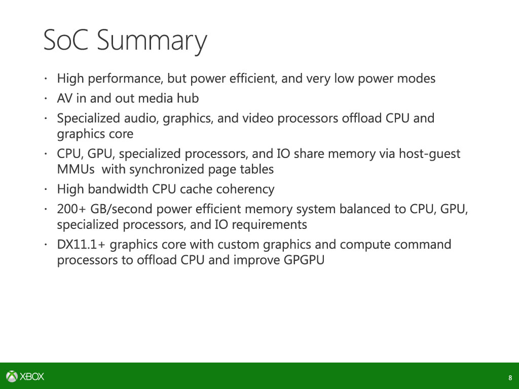
The hUMA and UMA concept is that they unify the addressing systems so the GPU and CPU can work on the same data at reduced cost and it's hardware managed so it has a reduced implementation cost. Wouldn't having a extra large cache like the eSRAM basically negate most of the benefits?
Based on the information available, it appears both CPU and GPU have a shared, coherent view of main memory, so that memory model has the same benefits you mentioned.
As far as the eSRAM goes, I don't think it has been stated by an official source, but let's go with the idea that it is a typical scratchpad memory, as has been claimed in this thread.
If so, the CPU and GPU still have a shared, coherent view of memory in the scratchpad (as an exclusive address space, the scratchpad cannot possibly be non-coherent). The challenge is actually the reverse: it is more difficult to have the CPU and GPU both use the scratchpad without sharing data. The address space of a scratchpad is not virtualized, so you need some way of partitioning - either spatially or temporally - to prevent one processor from clobbering another's data.
By the way, none of these systems are UMA. They are all NUMA, PS4 included.
Either the Move Engines have to shift data back and forth to enable GPGPU or the devs have to set aside an allotment of main memory and mark it CPU/GPU shared data.
This has been true of the GPUs internal scratchpad memory since the beginning, and presumably is still true with the GCN used here, with the exception that data sharing between cores is possible.