I doubt that complexity will go down with DDR4 at least not right from the start. Furthermore to achieve comparable speeds you need a bigger BUS which adds complexity aswell. Not sure but can't you just reserve eg. 256MB GDDR5 during standby and downclock it? That might not be as good as DDR4 but satisfy current laws. DDR4 will only be cheaper in the long run if the adaption rate is high enough - I am sure Sony will calculate if a eventual DDR4 refresh down the road will be worth sacrificing bandwith and trusted GDDR5 technology. After all who knows if in 2016 not GDDR7 will be the major GPU standard ;-)
Yes, DDR4 ultrawide IO would require a transposer but I expect it would be cheaper to use a transposer than the motherboard complexity and heat sink that GDDR5 would require. In any case if there is a second GPU it's likely that it will be on the same transposer the APU and memory will be on so a transposer is likely needed in any case.
Concerning the power issues I don't know enough except that yes DDR4 uses less voltage than GDDR5 but how this stacks up in real life I can't tell and I don't know how much power it would need.
GDDR5 would need a heat sink and can't be stacked more than 2 high while DDR4 can be stacked 8 high and with a wider interface. DDR4 ultra wide IO uses MUCH MUCH less power because it's designed to use less drive voltage and it can be clocked slower (in ultra wide IO configuration) yet still achieve the same bandwidth.
Power use is going to be a big issue in the near future, look at all the power saving features in AMD chipsets. Handhelds are leading the way with techniques to be more efficient and save battery life. These wide IO standards give DDRX memory 2Tb/sec bandwidth at maximum clock/power but at lower clock speeds, power efficiency at 200 mb/sec which is where we need to be to support the Sony CTO statements of 10X GPU and 300FPS video streams.
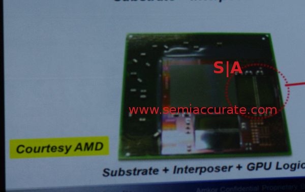
All the pictures and charts in my post above dealing with stacked memory except one are
AMD generated yet we are still discussing GDDR5 which can't be stacked. You and others are assuming OLD designs....you could be correct but I hope not.
There is no slide or drawing speculating GDDR5 for next generation game consoles but several for ultrawide IO DRAM which is assumed to be DDR4 but could be DDR3.
1)
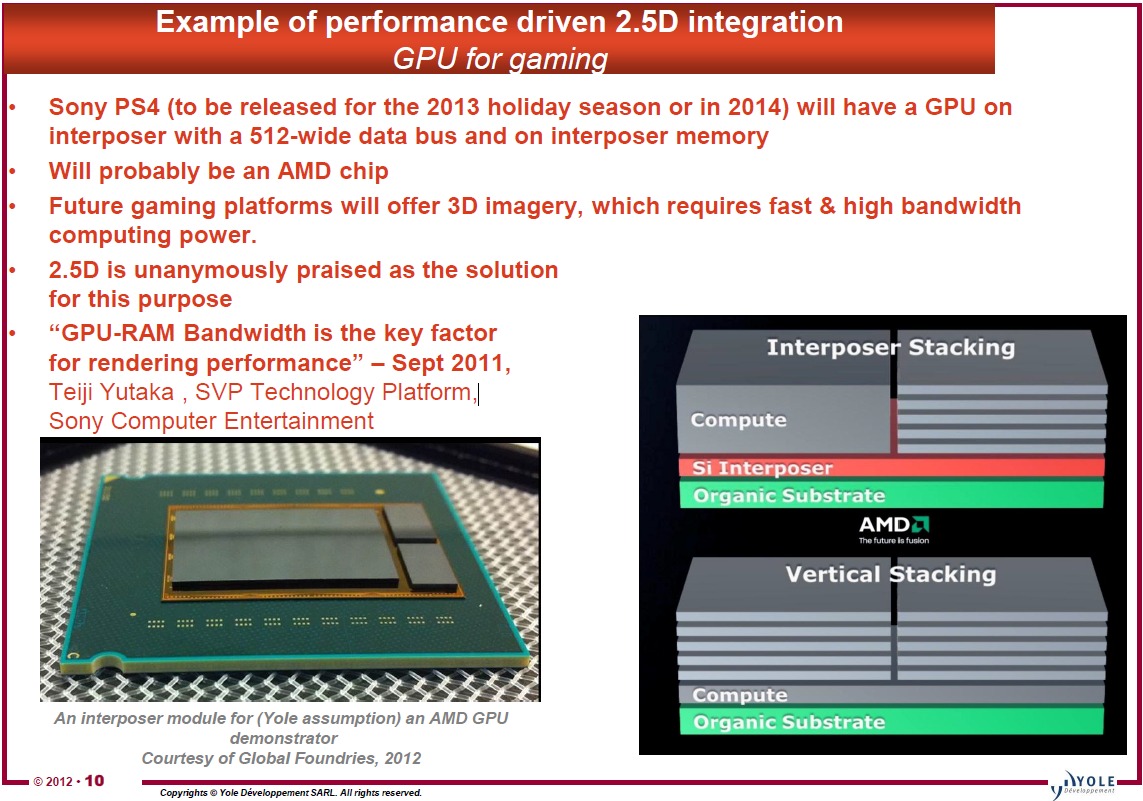
PS4 to have 2.5D stacked ultra wide IO memory
2)
Game consoles to have stacked ultra IO memory
Both of the above are informed speculation by the INDUSTRY, try to find anything for GDDR5 from the industry, plenty on NeoGAF and BY3D from supposed Leaks but nothing from the industry. Developer platforms are being used to project a PS4 design without thinking about the endgame requirements like mandated power rules for game consoles and always on server features. We have a fair idea of what the PS4 and Xbox 3 are going to support as well as target minimum specs from Sony Technology officers.
The following applies to the PS3 and Xbox 360 but next generation is assumed to be more powerful and consume more power so it needs even more power management to meet future mandated specs.
http://www.neogaf.com/forum/showpost.php?p=41486908&postcount=6 said:
Tier 3 standards Game Console Energy Star Requirements
Auto power off
Standby power .5W
Active navigation menu 35W
Active streaming Media 45W
The PS3 3000 chassis consumes
Standby .5W
Active Navigation Menu 61 watts
Playing game 72-79 watts
Xbox 360S Valhalla
Standby
67 watts at the dashboard
80 watts while gaming.
The last 4 PS3 refreshes had the following power savings: 20-10-5-4 The small numbers for the last few are because it's only been either RSX or Cell that had power savings not both at the same time. But do you see a trend, power savings is getting smaller with die size reductions it's not half or some ratio that's fixed. My impression is that just reducing from 45nm to 32nm is not going to reduce; Xbox for example, from 67 to 35 watts. The figures I used above are for the XMB menu where most of the power savings is in idle current. For full on game use the savings in die size reductions are (supposed to be) less (20-11-5-1). The last was PS3 3000 chassis where only the manufacturing technique for the Cell was changed.
Gong to 28nm is just about the same as 32nm so a move from 40nm to 28nm is not going to save 30 watts at the navigation menu (XMB) to comply with the current optional specs which I think will be mandated in little over a year. Certainly GDDR5 is going to exacerbate this while ultra wide IO DDR4 will use much less power than the PS3's memory.
Any refresh of Xbox 360 or PS4 from this point on and the PS4 and Xbox 720 will have to be designed to meet mandatory power requirements for game consoles. 20nm for PS3 by it'self, from the power savings trend above, is not going to meet the mandated standard either. It's going to take smart management of individual components (modern hardware) and ultrawide IO DDR4. So either the PS3 is dead next year or it's getting a total redesign to use modern hardware. The recent news of Sony selling the PS3 to China seems to indicate a longer life which implies a total redesign @ 20nm.
I've said this before and speculated that modern hardware would be used with the PS3 4K chassis and I was wrong, it didn't happen and power savings for the 4K chassis is only about 4 watts on my meter which is in the margin of error. The PS3 4K chassis and Xbox 360/S chassis can not be sold in California in a little over a year, what does this mean? They are to be discontinued soon after next generation is released or they are getting massive redesigns using modern hardware. If BC is provided in PS4 and Xbox 720 then a cut down version of newer console SoCs could work. It's possible that binned as defective PS4 SoCs with BC might work as PS3 SoCs.