• Hey, guest user. Hope you're enjoying NeoGAF! Have you considered registering for an account? Come join us and add your take to the daily discourse.

Next-Gen PS5 & XSX |OT| Console tEch threaD

Status
Not open for further replies.

SonGoku

Member
A) FLOP increase has slow down considerably
B) Prices of GPUs have gone dramatically upwards
C) Node shrinking has become harder and more expensive
You are just changing the argument now, but i dont mind
A) Not too much, but even taking into account 11TF (my prediction) is reasonable
B) Lack of competition
C) Yields improve and 6nm (refined 7nm) on the horizon
So no, we should not be expecting 11-13TF because there is a chip in PC out in 2w that is rated 225W with 9.75TF.
A bigger chip with lower voltage will net greater perf/watt
 

R600

Banned
I
Yes, but the graph is plotting costs taking into account yields on a brand new node, compared to the other nodes which are fully mature with high yields.. I wouldn't take that slide as fact going forward.
I seriously doubt that is what they are doing, this would be complete statistical failure which professional semiconductor firms dont do.
 

R600

Banned
You are just changing the argument now, but i dont mind
A) Not too much, but even taking into account 11TF (my prediction) is reasonable
B) Lack of competition
C) Yields improve and 6nm (refined 7nm) on the horizon

A bigger chip with lower voltage will net greater perf/watt
I am not changing argument. Every new gen is smaller jump then last, but this jump would be better then Gen 7 to Gen 8 compared to Gen 6 to Gen 7.

While you are at it, why not expect 48GB of RAM as we had 8GB last gen and 2x increase in 7 years is embarassing compared to last time? Or why not check raw perf of 2005 CPU and 8 Core Jag clocked at 1.6GHZ? I think Cell was actually more capable of the two, with 8 years on its back.

Bigger chip might get better perf/TDL sweetspot, but maybe going up 20mm² for same performance is less desirable then putting in better cooling? Perhaps console makers are not looking into die shrinking on next 2/3 nodes as it was the case in gen 7?

Your prediction is unreasonable because we HAVE actual Navi 10 chip that rates at 225W with 1.35TF and 8GB LESS then you are predicting for consoles. Not only that, Navi 10 is bigger chip then Pitcairn (212mm²) that ended up in PS4 with die size of 348mm² (without taking RT into account). For me, for anyone with simple math skills, this is completely unreasonable.
 
Last edited:

SonGoku

Member
I am not changing argument
If we get 11TF, let alone 13TF, that would be bigger jump then last gens
Every new gen is smaller jump then last.
Which is why im accounting 11TF not 14.4TF
but maybe going up 20mm² for same performance is less desirable then putting in better cooling?
Long term the bigger chip will be cheaper to produce than the power hungry one
Your prediction is unreasonable because we HAVE actual Navi 10 chip that rates at 225W with 1.35TF and 8GB LESS you are predicting for consoles
Because its pushing a higher voltage, hitting diminishing returns
Not only that, Navi 10 is bigger chip then Pitcairn (212mm²) that ended up in PS4 with die size of 348mm² (without taking RT into account).
Already posted die size calculations with RT HW included
 

R600

Banned
Which is why im accounting 11TF not 14.4TF

Long term the bigger chip will be cheaper to produce than the power hungry one

Because its pushing a higher voltage, hitting diminishing returns

Already posted die size calculations with RT HW included
And it would be. Last gen we had actually more potent CPUs then this gen, which is apsurd.

It remains to be seen what "power hungry" means, doesnt mean Navis hit same GCN voltage/clock cliff. If not, then certainly smaller chip with higher clocks (even at slight loss of perf/watt) will surely be less expensive.

Everyone talks about new nodes being more expensive, yet you fail to address it and wave it off as if its just yields issue.

This is from Mark Papermaster :

“Moore’s Law is slowing down, semiconductor nodes are more expensive, and we’re not getting the frequency lift we used to get,” he said in a talk during the launch, calling the 7-nm migration “a rough lift that added masks, more resistance, and parasitics.”

No, calculation does not tell us that. Its very shoddy done.

If such calculation works, how come PS4 SOC is 348mm² with smaller GPU (20CU pitcairn is 212mm² instead of 251mm² with 40CU Navi), 8 cord Jaguar and no RT cores? Certainly if Pitcairn is only 212mm² for 20CU we can fit another 20 in 348mm²?
 

SonGoku

Member
Last gen we had actually more potent CPUs then this gen, which is apsurd.
Last gen CPUs were trash at CPU tasks, so no not really
Everyone talks about new nodes being more expensive, yet you fail to address it and wave it off as if its just yields issue.
When comparing different die sizes on the same process node yields are the number one factor driving costs
Not talking of chip design which does get more expensive.
If such calculation works, how come PS4 SOC is 348mm² with smaller GPU
uhm because im working with a 380-390 mm2 die not 348mm2
and we’re not getting the frequency lift we used to get,
This is what i've been parroting, 7nm power reduction is poor. Its strength is on the density increase
 
Last edited:

FrostyJ93

Member
I hope the scarlett casing is dual tone like One S. White body with black base. Its been really popular with One S and the robot white version of One X. I feel like its kinda become iconic for xbox and would help differentiate scarlett from the likely single tone PS5.
 

vpance

Member
Its not only yields, there is clear pattern of each new node being more expensive one.


Apparently Sony got that memo as well since their chip die sizes are following this trend, backwards.

If true, then we better prepare ourselves for $500 8TF 😟🔫
 
Last edited:

R600

Banned
Last gen CPUs were trash at CPU tasks, so no not really
They weren that bad. Certainly, Cell was a good match to 8yr younger CPU (albeit mobile one)

When comparing different die sizes on the same process node yields are the number one factor driving costs
Not talking of chip design which does get more expensive.
Well 5minutes of googling tells you all costs have gone up with node shrinking. There is a reason why there are only really TSMC and Samsung left from 3rd party manufacturers. Costs are booming, and Sony regression in die sizes follows node shrinking tit for tat.

uhm because im working with a 380-390 mm2 die not 348mm2
But you are assuming best case scenario for Scarlett (which might be bigger chip then PS5s anyway). It can range anywhere from 338mm² to 400mm².

Reason why I am asking you about PS4 is because they only where able to fit Pitcairns 20CUs (212mm² GPU) inside PS4s 348mm² die, but you expect 50% increase from Navi10 40CUs (251mm² GPU) with RT hardware bolted for a good measure.

This is why this math is just completely off.
 

R600

Banned
If true, then we better prepare ourselves for $500 8TF.
This is true. This has been talked about for last 5 years. Each new node is more expensive then last one. From design to production, verification and yields, its getting worse and worse.

This is why GPU costs have gone up so much compared to 10yrs ago (well, along with Nvidia dominating).

But AMD showed normalized wafer cost have gone 100% from 28nm to 7nm, which is obviously huge.
 
Last edited:

SonGoku

Member
They weren that bad. Certainly, Cell was a good match to 8yr younger CPU (albeit mobile one)
Cell helped with GPU tasks, it was trash at traditional CPU tasks, Jaguar definitely has it beat on that
Well 5minutes of googling tells you all costs have gone up with node shrinking. There is a reason why there are only really TSMC and Samsung left from 3rd party manufacturers. Costs are booming, and Sony regression in die sizes follows node shrinking tit for tat.
You are misinterpreting the data. That affects chip design, those costs you mention are the same irrespective of size
What determines smaller dies is yields
TT9a_575px.png

But you are assuming best case scenario for Scarlett (which might be bigger chip then PS5s anyway). It can range anywhere from 338mm² to 400mm²
All estimates i read are 370mm2 upwards
I believe both consoles will be evenly matched which means similar size
Reason why I am asking you about PS4 is because they only where able to fit Pitcairns 20CUs (212mm² GPU) inside PS4s 348mm² die, but you expect 50% increase from Navi10 40CUs (251mm² GPU) with RT hardware bolted for a good measure.
CUs take less than 50% die space, its not a linear scale and they've got much smaller since 2012.
This is why this math is just completely off.
I posted the math for each component, feel free to tell me where is off
 
Last edited:

SonGoku

Member
If true, then we better prepare ourselves for $500 8TF.
But while EUV is expected to reduce the cost of manufacturing processors by cutting the number of masks required per design, it does nothing to reduce the cost of designing the chip in the first place — and chip design costs are rising so quickly, they could effectively kill long-term semiconductor scaling across the entire industry.
Its not related to die size
 
Last edited:

TLZ

Banned
Well 1 DCU is 2CUs... so yes it does the work of 2 CUs.
They just combined two CUs to use the same cache... the CUs are actually the same yet with 64 Shaders.
That is very interesting indeed. Isn't this a big thing? Instead of 1 occupying the cache, 2 can? Easily doubling the teraflops sharing the same cache? And efficiency of course.
 
Found this slide:

03_o.jpg
This probably explains why early (non-EUV) 7nm is so expensive:

07_o.jpg


Too many lithography steps, it seems EUV (far fewer steps) is a must to bring it back on track cost-wise.

The etching quality difference is humongous, even to the naked eye:

8.png


I'm pretty sure EUV etched circuits will need less voltage for the same performance and it will reduce leakage as well.
 

SonGoku

Member
This probably explains why early (non-EUV) 7nm is so expensive:

07_o.jpg


Too many lithography steps, it seems EUV (far fewer steps) is a must to bring it back on track cost-wise.

The etching quality difference is humongous, even to the naked eye:

8.png


I'm pretty sure EUV etched circuits will need less voltage for the same performance and it will reduce leakage as well.
Interesting
I see two equally likely scenarios
  1. Eat losses with Big 7nm die then shrink to 6nm on 2021 for cost reductions.
  2. Launch using 7nm EUV from the start
 
Last edited:
"Complex exposure processes push up costs

The cost jumps up with the 7nm process because it is more unreasonable in the process steps. 7 nm of TSMC uses the existing ArF excimer laser light source for exposure technology. ArF, which has a wavelength of 193 nm, enables patterning to 80 nm or less, with a minimum pitch of 76 nm, using immersion exposure technology that uses liquid refraction to increase resolution.

Conversely, immersion single patterning (LE) can only cut to 76 nm pitch. In the case of 7 nm of TSMC, the minimum metal pitch (wiring distance) is 40 nm, which can not be handled. Therefore, it is necessary to carry out finer processing using multi-patterning technology.

Specifically, “Self-Aligned Quadruple Patterning”, which is a very complicated process, is used to generate the fin of the narrowest transistor, and “SADP (Self- Use “Aligned Double Patterning” etc.

Such multi-patterning technology is complicated in process and requires the number of masks. In addition to the cost of the mask, as the number of masks increases, the factor of decreasing the yield increases. Also, process control such as overlay and CD (Critical Dimension) control becomes difficult. As a result, the total manufacturing cost is pushed up.

This is the problem with current advanced processes. However, even at the node named 7 nm, the situation changes when it comes to EUV (Extreme Ultraviolet) exposure. Since the number of masks is drastically reduced, the cost is lower in principle, the yield can be easily increased, and the process control can be facilitated.

TSMC adopts EUV with next-generation 7nm "7FF +", and Samsung has already prepared 7nm of EUV version. In the EUV 7 nm, since the EUV device itself is expensive, it is necessary to initially consider the cost of device depreciation. However, in the long run, the EUV generation is expected to have lower costs. That is, the EUV version 7 nm process migration reduces cost to some extent. The current ArF immersion 7 nm process is the most expensive process."


Source: https://pc.watch.impress.co.jp/docs/column/kaigai/1156455.html

ASML (a Dutch company) is the only one that produces cutting-edge photolithography equipment:


To put it in layman's terms, it's like buying an expensive "printer" that will print high-res copies more easily, so in the long run each copy should cost less, despite the initial investment. :)

TL;DR: non-EUV 7nm is a mistake.
 

LordOfChaos

Member
Early Zen 2 review may have broken NDA here. But ST performance is all but at the heels of the best, and this is with 6 cores, the 8 core model should be up there in MT too. Clock speeds will be tamped down for a console, but for the same wattage level, we really wouldn't be losing much compared to what Chipzilla could offer.

 
Last edited:
the Zen in the consoles is the x570 right? which would be even better than the one in the leak? If the console cpus are at that level....then thats pretty damn exciting.
 

ethomaz

Banned
That is very interesting indeed. Isn't this a big thing? Instead of 1 occupying the cache, 2 can? Easily doubling the teraflops sharing the same cache? And efficiency of course.
There isn’t doubling the teraflops.
The shared cache I believe just means less silicon used... smaller CUs.
 
Last edited:
was here in 2012. Know what folks expected? 2.5-3TF machines. Why? Because EPIC had hard on on "2TF is minimum for next gen, we are urging Sony/MS to listen".

What happened? We got 1.2TF Xbox and 1.8TF PS4. Both well below expected, Xbox embarassingly so (back then 4TF was highest rated GPU)
Crytek had asked for 8GB of RAM since 2011:


Since you've been here since 2012, you'll probably remember how many people were low-balling at 2GB of RAM (4x vs 7th gen seemed huge back then) and 4GB was considered "optimistic".

Regarding Teraflops, we got laptop chips (Jaguar + 7970M for PS4, don't remember the XB1 GPU equivalent). That's a fact. 7th gen incurred huge losses for both companies (5 billion $$$ for Sony alone), not to mention MS losing at least 1 billion $$$ due to RROD. They didn't want to risk it, at least not during an economic recession (luckily those days are behind us). And let's not forget the doom & gloom climate regarding "dying" consoles vs the glorious PCs.

Lots of people ate crow with how 8th gen played out eventually. ;)

Try to think what would have happened if MS had went big from the get-go and actually practiced the Scorpio philosophy (Hovis method aka tailored undervolting per chip, vapor chamber cooling, huge gaming-focused die, GDDR5, no eSRAM/TVTVTV/DDR3) at 28nm (since 16nm FinFET wasn't available).

3TF (half of Scorpio Engine at 16nm) would have been totally realistic and maybe the generation/resolution warz would have played out differently. We will never know (maybe this branch of history materialized in a parallel universe).

All in all, it's probably not very wise trying to predict 2020 consoles with 2013 data. Times have changed. That's also why you don't see pie in the sky/unrealistic predictions like 128GB of RAM (yet another 16x increase).
 

kegkilla

Banned
Crytek had asked for 8GB of RAM since 2011:


Since you've been here since 2012, you'll probably remember how many people were low-balling at 2GB of RAM (4x vs 7th gen seemed huge back then) and 4GB was considered "optimistic".

Regarding Teraflops, we got laptop chips (Jaguar + 7970M for PS4, don't remember the XB1 GPU equivalent). That's a fact. 7th gen incurred huge losses for both companies (5 billion $$$ for Sony alone), not to mention MS losing at least 1 billion $$$ due to RROD. They didn't want to risk it, at least not during an economic recession (luckily those days are behind us). And let's not forget the doom & gloom climate regarding "dying" consoles vs the glorious PCs.

Lots of people ate crow with how 8th gen played out eventually. ;)

Try to think what would have happened if MS had went big from the get-go and actually practiced the Scorpio philosophy (Hovis method aka tailored undervolting per chip, vapor chamber cooling, huge gaming-focused die, GDDR5, no eSRAM/TVTVTV/DDR3) at 28nm (since 16nm FinFET wasn't available).

3TF (half of Scorpio Engine at 16nm) would have been totally realistic and maybe the generation/resolution warz would have played out differently. We will never know (maybe this branch of history materialized in a parallel universe).

All in all, it's probably not very wise trying to predict 2020 consoles with 2013 data. Times have changed. That's also why you don't see pie in the sky/unrealistic predictions like 128GB of RAM (yet another 16x increase).
Pretty sure we only got 8gb because memory prices took a big dive in the months leading up to the start of production.
 
Just look at PS4Pro with 320mm² die on 16nm node. It was smaller die, but system cost more then PS4 with bigger die because cost per mm² went up with each smaller node.
Source?

PS4 Pro has a lower BoM cost (around $321, IIRC) compared to OG PS4. The fact that it has half the amount of DRAM chips drops the cost quite a bit. OG PS4 shipped with 16 DRAM chips.

If anything, consoles have a trend to increase the DRAM budget, not decrease it (XBOX 360 had only 4 GDDR3 chips at 128-bit, same for PS3 RSX).

OG PS4 and XB1 increased the DRAM bus to 256-bit and the number of DRAM chips (both for GDDR5 and DDR3) to 16.

Scorpio increased the bus to 384-bit. I don't think it's unrealistic to expect 24GB 384-bit for $499 (MSRP) consoles. 512-bit would be too much (heat-wise), so I don't expect it.

Sony didnt even put in UHD because they wouldnt be able to sell it for $400.
They did this because: 1) movie streaming has taken over the market, 2) BDXL discs for PS4 games wouldn't make sense (it would break BC with OG consoles).

PS5 will have BDXL 100GB discs for next-gen games, first and foremost. Supporting physical UHD movies as well will be an added bonus.

Notice how XBOX is trying to paint a digital-only narrative (with Game Pass) and how contradictory is to tout physical UHD movie discs at the same time... does it make sense marketing-wise?

It's the very definition of a confusing message.

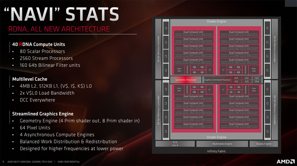
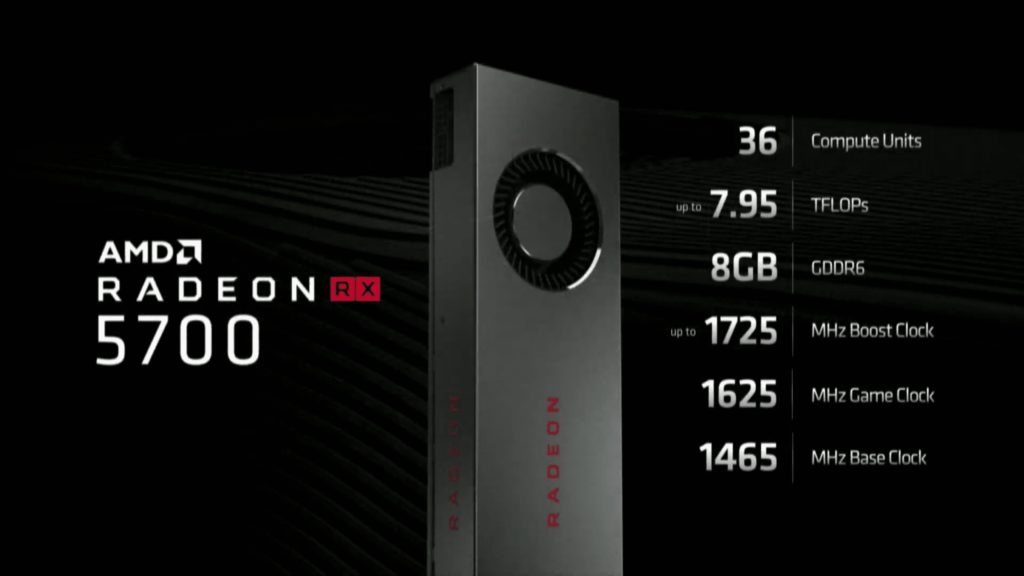
So how do we get chip with Zen2, ~ Navi 5700, Ray Tracing, 16GB of GDDR6, UHD and 1TB of SSD for $400? We dont. And we wont.
Nobody in their right mind expects $399 consoles this time around. Personally, I don't even expect a $499 BoM cost. These consoles will have to be sold at a loss, that's a given.

I've clarified my position, since I don't want to be accused of "unrealistic expectations" (offering high-end hardware for $399 and making a profit at the same time a la 2013).

Pretty sure we only got 8gb because memory prices took a big dive in the months leading up to the start of production.
Who's to say that GDDR6 chips won't take a similar dive? Samsung has already announced 2GB chips with 60% lower consumption (newer lithography/less costs).

I don't think we need 32GB (unless they go with a 2TB HDD + NAND cache), 24GB seems the best compromise for an SSD-only system and it will provide a big fat bus for the GPU.

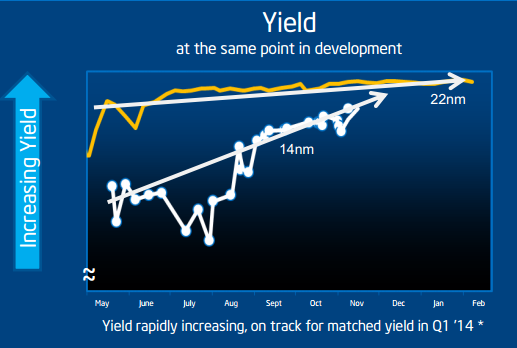
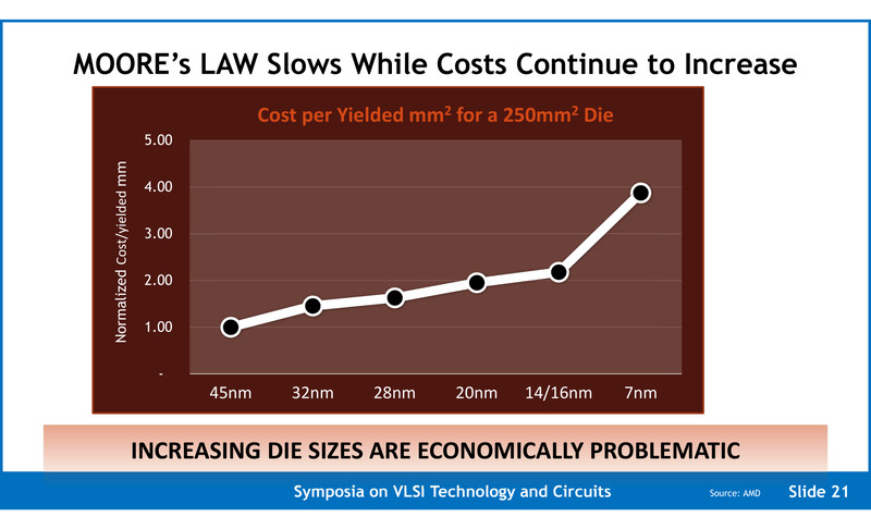
I really don't think that is about yields. Yields always start poor(ish) and then improve. That article is clearly describing a new phenomenon (part of the end of Moore's Law).
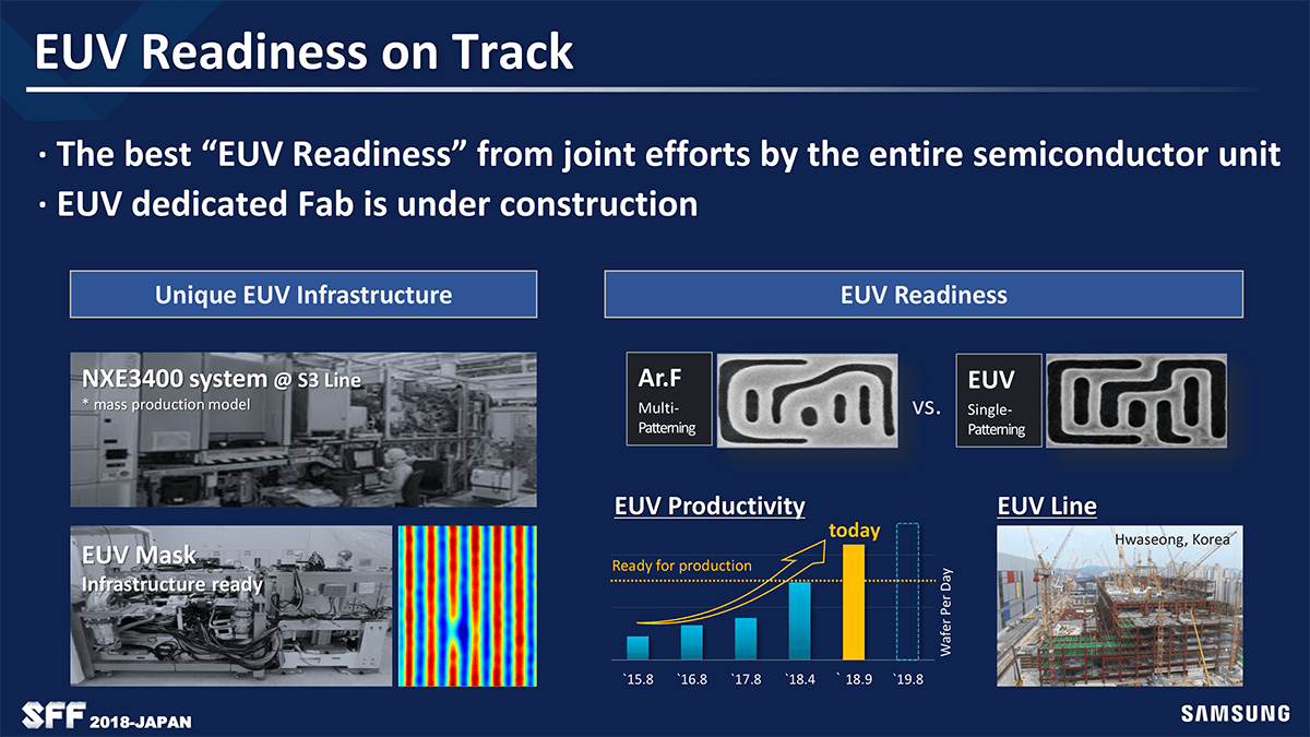
EUV will accelerate Moore's Law once again and the silicon will be alive and kicking for a long time:

Screenshot_2019-05-09-5nm-Pesquisa-Google.png


I don't think people realize how important EUV is for the entire tech industry.

2nm will be probably ready for the PS6 (last gen of physical consoles, then it's all about the cloud and 3D die stacking).


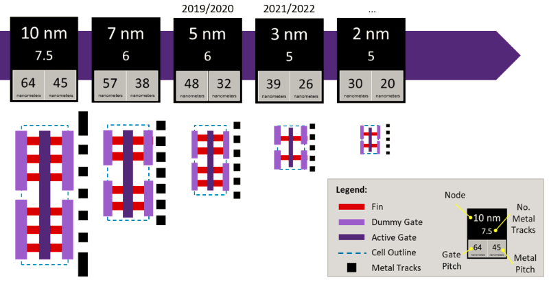
I'm not arguing anything. The article I posted is saying, leaving aside yields, that a 250mm^2 chip costs twice as much as the previous node. This puts huge pressure on the console makers to limit as much as possible the size of their SoCs

At least that is my running logic here.
It will be a huge mistake to limit consoles with a 10-year lifecycle (2020-2030), only because of 1st gen 7nm poor yields with multi-patterning.

They either have to subsidize huge 400mm2 dies (expect 200W+ consoles) or just wait for TSMC's 2nd gen 7nm with EUV (that's the refined 6nm/N6 process from what I understand).

If you refer to the Pro, they had a goal in mind and they met it. The Pro is likely never udergoing a shrink so it makes sense to make the chip as small as possible. Thats not the case with PS5
Both PS4 Pro and XB1X will likely be EOL by late 2020.

They're consoles aimed at enthusiasts and PS5/SNEK will make them irrelevant.

PS4/XB1 Super Slim will still be relevant for casuals, so a 7nm die shrink (tape-out costs around ~250 million) makes financial sense.

And now look how entire graphics sector has moved from 2005 to 2013 in terms of FLOPS (0.2 to ~4) and from 2013 to 2020 (4 to ~ 14) and you will notice that :

A) FLOP increase has slow down considerably
B) Prices of GPUs have gone dramatically upwards
C) Node shrinking has become harder and more expensive
A) Moore's Law hasn't slowed down when it comes to GPGPUs. You have to also take into account INT8/FP16 increases, which will be quite useful for next-gen AI. Rasterization isn't the only thing consoles are meant to perform.


B) Because of mining and Nvidia being a tad bit greedy:


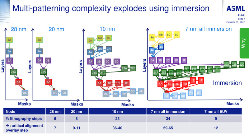
C) EUV will replace multi-patterning and Moore's Law will keep progressing just fine.

Multi-patterning is just not viable for sub-10nm nodes.

Or why not check raw perf of 2005 CPU and 8 Core Jag clocked at 1.6GHZ? I think Cell was actually more capable of the two, with 8 years on its back.
It wasn't:


We got a 30-watt octa-core CPU at 28nm (Jaguar at 1.6 GHz) and we're also getting a 30-watt octa-core CPU at 7nm (Zen 2 at 3.2 GHz).

Not many people realize this, but die and TDP budget is the same in both cases. The lion's share will still be consumed by the GPU, as always.

ps: I'm old enough to remember the "death" of transistor scaling since the 80s at least. Back in 2000 I remember engineers saying that 30nm is the lowest we can expect and yet, we got 28nm consoles in 2013.

This is true. This has been talked about for last 5 years. Each new node is more expensive then last one. From design to production, verification and yields, its getting worse and worse.

This is why GPU costs have gone up so much compared to 10yrs ago (well, along with Nvidia dominating).

But AMD showed normalized wafer cost have gone 100% from 28nm to 7nm, which is obviously huge.
That's why exotic chips like Cell have been abandoned and that's why we might also see a Sony/MS hardware collaboration in the future.

Why pay AMD twice for doing R&D? They can share the costs and increase economies of scale even further, more so if they think Google Stadia is against their interests.

They clearly think that it's pointless to invest on 2 separate cloud infrastructures (multi-billion dollar ventures) and that's why they collaborate on Azure.

What was unthinkable back in 2013 is totally realistic these days.
 

SonGoku

Member
2nm will be probably ready for the PS6 (last gen of physical consoles, then it's all about the cloud and 3D die stacking).
I dont think physical console hw will ever disappear, traditional clear cut gens maybe.
Cloud gaming uses a fixed spec, might as well profit both ways cloud + physical. Not to mention as the fixed spec goes higher the cost of cloud servers gets exponentially higher.
and what about latency? are they going to have server farms in each small town?
PS4 Pro has a lower BoM cost (around $321, IIRC) compared to OG PS4. The fact that it has half the amount of DRAM chips drops the cost quite a bit. OG PS4 shipped with 16 DRAM chips.
He later clarified he meant soc cost 🤷‍♂️
It will be a huge mistake to limit consoles with a 10-year lifecycle (2020-2030), only because of 1st gen 7nm poor yields with multi-patterning.
Precisely
They either have to subsidize huge 400mm2 dies (expect 200W+ consoles) or just wait for TSMC's 2nd gen 7nm with EUV (that's the refined 6nm/N6 process from what I understand).
7nm EUV and 6nm are different but both are 7nm with EUV layers.
  • 7nm EUV offers power reductions and slightly greater density than 6nm 20% vs 15-18%
  • 6nm only offers increased density (no power reductions) but has the advantage of being design compatible with 7nm finfet meaning chip designs can be shrunk with minimal investment for quick cost reductions
The options are:
  1. Launch from the start on 7nm EUV 330 mm2 chips (equal to 400 mm2 7nm chips) - best performance
  2. Launch on 7nm, eat losses on big chip until it can be shrunk to 6nm
A) Moore's Law hasn't slowed down when it comes to GPGPUs. You have to also take into account INT8/FP16 increases, which will be quite useful for next-gen AI. Rasterization isn't the only thing consoles are meant to perform.
dont forget integer instructions can aid rasterization too (up to 36%)
 
Last edited:
I dont think physical console hw will ever disapear, traditional clear cut gens maybe.
Physical consoles and media will go the way of vinyl records sometime in 2030-2040.

Will they exist? Maybe, but it will be an expensive and niche product for collectors, just like audiophiles spending exorbitant amounts of money on vinyl records + equipment.

Cloud gaming uses a fixed spec, might as well profit both ways cloud + physical. Not to mention as the fixed spec goes higher the cost of cloud servers gets exponentially higher.
2nm will probably be the end of the road for traditional silicon, 1nm might not even work due to quantum tunneling phenomena.

What's next? You either stack lots of low-power silicon dies in a 3D manner (think of the HBM equivalent for processing chips) and use industrial-grade cooling or graphene chips or quantum computing...

and what about latency? are they going to have server farms in each small town?
I imagine they will have servers in every country.

Tech is improving, that was back in 2012 with Kepler GPUs:

gridlag2.png


dont forget integer instructions can aid rasterization too (up to 36%)
And foveated rendering/variable rate shaders.

The discussion is all about FP32 performance and comparing FP32 numbers in different generations, but once again, we will have huge architectural improvements (fixed-function T&L -> pixel/vertex shaders -> unified shaders -> compute shaders -> mixed-accuracy compute shaders).
 

SonGoku

Member
Physical consoles and media will go the way of vinyl records sometime in 2030-2040.

Will they exist? Maybe, but it will be an expensive and niche product for collectors
The reason why this doesn't make sense to me is that, you'll need an electronic device regardless and in 2040 technology will be far enough were you can have all the hw required on a tiny box, built into your TV and maybe even on your phone.
It will be cheaper to use/produce local hw.
2nm will probably be the end of the road for traditional silicon, 1nm might not even work due to quantum tunneling phenomena.

What's next? You either stack lots of low-power silicon dies in a 3D manner (think of the HBM equivalent for processing chips) and use industrial-grade cooling or graphene chips or quantum computing...
And you cant use post silicon technology on local hw why exactly?
Tech is improving, that was back in 2012 with Kepler GPUs:
Physical distance will always be a limitation.
 
Last edited:
The reason why this doesn't make sense to me is that, you'll need an electronic device regardless and in 2040 technology will be far enough were you can have all the hw required on a tiny box, built into your TV and maybe even on your phone.

It will be cheaper to use/produce local hw.

And you cant use post silicon technology on local hw why exactly?
If die shrinks stop happening sometime in the future, the only way to keep increasing the processing power with traditional silicon will be to use more chips in a 3D stacking manner, which will increase cost, TDP and cooling requirements.

Energy consumption in datacenters might not even be an issue in 2040, assuming we will have tackled cold fusion by then.

But having noisy and expensive boxes at home will certainly be a problem...

I don't think you can have an affordable home console if you will be forced to stack for example 10-20 GPU chiplets and their accompanying HBM for each one.

IBM is doing some research on exotic cooling methods: https://phys.org/news/2010-03-years-3d-chip-stacking-law.html

Graphene promises THz speeds (it would be king for ST applications), but we haven't seen any implementations yet and quantum computing has a long way to go in terms of increasing qubits, let alone cooling requirements and who knows if governments would allow every citizen to have a quantum computer and be able to trivially break almost any encryption that we use in the market.

Physical distance will always be a limitation.
Yeah, that's why it needs a dense network globally and FTTH connections (<1ms first-hop ping), not to mention that they would have to abolish bandwidth caps (5G promises to deliver that).
 
Last edited:

SonGoku

Member
If die shrinks stop happening sometime in the future, the only way to keep increasing the processing power with traditional silicon will be to use more chips in a 3D stacking manner, which will increase cost, TDP and cooling requirements.
I dont know Rick, i think even 3D stacking will be a paradigm shift that'll lower costs and heat (HBM takes less space, its faster and more power efficient), and what about all the post silicon tech/materials
Quantum computing is the future anyways and in that future you'll have all the hw required to run games on your watch probably :messenger_tears_of_joy:

Whatever future cloud gaming has, it'll be short lived. Its costs are too high in the long term and new technologies will make it obsolete.
Yeah, that's why it needs a dense network globally and FTTH connections (<1ms first-hop ping), not to mention that they would have to abolish bandwidth caps (5G promises to deliver that).
So server farms in every small town?
 
Last edited:

ethomaz

Banned
Well shouldn't smaller CUs mean we can fit more in there, thus higher TFs at similar clock speeds?
Yes but the estimates are based in Navi CU size already.

Plus with RT hardware they will probably become bigger than actual Navi CUs.
 
Last edited:
  • Like
Reactions: TLZ

sinnergy

Member
These reveals will not be about TF, instead the will be about game technology and what’s possible to tell a story with outstanding visuals. And maybe about ray-tracing how good it is to ground your game in reality. Mark my words.
 
I dont know Rick, i think even 3D stacking will be a paradigm shift that'll lower costs and heat, and what about all the post silicon tech/materials
Quantum computing is the future anyways and in that future you'll have all the hw required to run games on your watch probably :messenger_tears_of_joy:
I edited my previous post. I don't think quantum chips will be small enough to fit in a watch, cooling requirements are insane for just a few qubits, but maybe we're in the ENIAC stage of the quantum computing era.

Whatever future cloud gaming has, it'll be short lived. Its costs are too high in the long term and new technologies will make it obsolete.
Cloud gaming is all about control and reducing costs for companies.

100 million PS4s serve 100 million customers. Do they work all the time? Clearly not, so it's not "efficient" (notice all the ecology/green computing/CO2 discussions these days).

100 million cloud-based consoles will likely serve 500 million customers (1:5 oversubscription ratio).

See the difference? They can serve a lot more people with far fewer machines, so it's cheaper for them.

Their projections say that they will need to serve 2-5 billion gamers in the future. Massive investments are needed and you can only manufacture 2-3 million home consoles per month, so do the math.

To give you an analogy, cloud gaming in virtualized machines is the equivalent of public transportation for gaming. Home console ownership is the equivalent of owning a car.

Which one is more efficient for the masses (billions of gamers)? Sharing infrastructures is always more efficient, at the expense of ownership.

So server farms in every small town?
It depends on the country.

Iceland for example will just need a few servers in the capital, it's a small island of 300K people. No need to have servers in every village, the whole island is connected with optical fibers (<1ms) since the 80s. One frame is 16-33ms.

USA on the other hand is a big country with huge geographical distances, you'll need servers in West Coast (Cali), in East Coast (NYC) etc.
 
Last edited:
Why are people basing off their speculation on off the shelf navi cards? I am sure cerny and the guys are cooking new means of getting past the shitty limits of the navi. Navi right seems like a shitty fucking card overall. Very expensive and doesnt make good use of the potential of the 7nm.

Why the fuck would sony use this shit on their next gen console when they have better tech coming up. Seems like a wasted opportunity. 10-11 tf is all i ask for for longivity plz.
 
So if we're looking at Navi dual compute units (2 CUs must be disabled at a time) then it makes sense to alter the number of shader engines too to increase yield?

Something like:
  • 64 CU die
  • 4 shader engines
  • 1 dual CU disabled per shader engine to increase yield - tolerate 1 fault per shader engine
  • 64 - (4x2) = 56 CUs active

just to clarify: it's not that likely to get more than one defect per die if defect density is moderate. if you get two or more defects per die it's not very likely that they affect just the CUs. till now AMD disabled 1 CU per shader engine to keep load symmetry intact (same performance potential per SE).


which brings us to Navi. it seems like something has chganged:

2acaceff-ff7a-4d53-91ee-2cd71d23fd7e.PNG


if you have to disable one dual CU per SE* there shouldn't be a rx 5700 (with 36 CUs instead of 40 CUs of the 5700 XT) but just a 32 CU card. so maybe you now can disable half a dual CU or you mustn't disable symmetrically anymore.


*a bit of caution: the definition of a shader engine might have shifted with navi also.
 

sinnergy

Member
Why are people basing off their speculation on off the shelf navi cards? I am sure cerny and the guys are cooking new means of getting past the shitty limits of the navi. Navi right seems like a shitty fucking card overall. Very expensive and doesnt make good use of the potential of the 7nm.

Why the fuck would sony use this shit on their next gen console when they have better tech coming up. Seems like a wasted opportunity. 10-11 tf is all i ask for for longivity plz.
Because there is no other supplier that offers adjustable socs this way.. that’s why..
 

SonGoku

Member
100 million cloud-based consoles will likely serve 500 million customers (1:5 oversubscription ratio).
In 50 years the tech will be so advanced smartphones will be powerful enough. Gaming will be decentralized so you'll probably game on any device you already own. Newer devices higher presents and framerates.
Their projections say that they will need to serve 2-5 billion gamers in the future. Massive investments are needed and you can only manufacture 2-3 million home consoles per month, so do the math.
Ok so traditional consoles will be gone and instead it will be seamless where you can game on your computer, phone, tablet, console type media box.

If the costs for local hw skyrocket the same will happen to cloud hw
USA on the other hand is a big country with huge geographical distances, you'll need servers in West Coast (Cali), in East Coast (NYC) etc.
To beat the physical limitation that's not enough, how would you even play 8k+ VR games
I edited my previous post. I don't think quantum chips will be small enough to fit in a watch
Yeah but eventually they will and then there's the other post silicon materials that yourself mentioned will make cloud computing obsolete
Cloud gaming has a future but it ain't the future.
if you have to disable one dual CU per SE* there shouldn't be a rx 5700 (with 36 CUs instead of 40 CUs of the 5700 XT) but just a 32 CU card
5700 is a small chip with only 2SEs that's why,
Bigger chips will use 4SE
 
Last edited:

R600

Banned
Gonzalo overall 3DMark score :


Ryzen7 2700 with RTX2070 score :

~20-24K in 3DMark11
~20K in Firestrike.

Ryzen 2700 with Vega56 score :

~20-25K in 3DMark11
~19K in FireStrike

I expect Gonzalo to be around 8.5TF. Perhaps 8.3TF with 1.8GHZ and 36CU is exact number ;)
 
Last edited:

R600

Banned
3DMark :
PS4 Pro - Rough score 5000
Gonzalo - score 20000 up


5000 i think it's not possible for base PS4.
Yea not sure, might be older bench.

Best to compare these scores to overall scores of Zen 2700 and 2070/Vega56 in 3DMark 11 and Firstrike. That should be ballpark, and from what I can see, it should be slightly better then Navi 5700 (that one scored only 3% shy of 2070)
 

CrustyBritches

Gold Member
3DMark :
PS4 Pro - Rough score 5000
Gonzalo - score 20000 up


5000 i think it's not possible for base PS4.
Tweet that came from...
apisak_tweet.jpg


Seems like Firestrike by the range he's describing. Not getting the graphics score, only the combined result. AMD does really well in this benchmark and that's right in the wheelhouse of the Vega 56 with Ryzen 2700X CPU. Will wait for more details.
 
Status
Not open for further replies.
Top Bottom