• Hey, guest user. Hope you're enjoying NeoGAF! Have you considered registering for an account? Come join us and add your take to the daily discourse.

Next-Gen PS5 & XSX |OT| Console tEch threaD

Status
Not open for further replies.

SlimySnake

Flashless at the Golden Globes
Vega @ 1800MHz with 12.9Tf to emulate 1.8GHz Navi ~8-9TF with RT fits like a glow.

Sorry, just cant take 13TF Navi leaks seriously. Its far, far too big and power hungry for console. I understand these kind if leaks have started before we knew what Navi actually brings.
right. that makes sense to me too. it also fits the Andrew Reiner leak where he said the devs told him ps5 had more flops. its entirely possible that the devkits were using vega 56 at 1.8ghz.

RX 5700XT is way too power hungry for anything over 9-10 tflops in a console. lets hope its just a shit half baked design from AMD just to get it out. the die has a lot of empty space and releasing a 250mm2 card for $449 doesnt make much sense. its possible they just released it to have something out this year.
 

xool

Member
I meant how do you type the tiny square 2

On windows you can get ² by typing ALT(hold) and 0178 on the numeric pad (not top row) .. remember to leave NumLock on ..

That's an interesting one (maybe legit)

Vega @ 1800MHz with 12.9Tf to emulate 1.8GHz Navi ~8-9TF with RT fits like a glow.

Sorry, just cant take 13TF Navi leaks seriously. Its far, far too big and power hungry for console. I understand these kind if leaks have started before we knew what Navi actually brings.

Either fake leakers are just copypasting, or there's something in those 12.8/12.9TF leaks - keeps coming up in the better looking leaks.

I agree we're now looking at a smaller number on Navi, equivalent in 'graphics quality' to the 13TF Vega..

...maybe Penello was right all along with his 8TF PS5 after all..
 
Last edited:

SonGoku

Member
On windows you can get ² by typing ALT(hold) and 0178 on the numeric pad (not top row) .. remember to leave NumLock on ..
on laptop so no numpad
Ms office it is! lol
...maybe Penello was right all along with his 8TF PS5 after all..
Panello was lowballin PS5 with 8TF while hyping 12TF xbox.

I dont pay much attention to leaks anyways, just look at whats doable on 7nm
380-390 mm2 APU should net anywhere in between 11-12TF with decent cooling
 

THE:MILKMAN

Member
I think.......

1, The Reiner Tweets are referring to target (retail) specs in the written documentation not to current dev kits specs.

2, Next consoles will fall into the 8-9.5TF bracket and perform equal to Vega 64/1080.

ETA: Clarification
 
Last edited:

R600

Banned
right. that makes sense to me too. it also fits the Andrew Reiner leak where he said the devs told him ps5 had more flops. its entirely possible that the devkits were using vega 56 at 1.8ghz.

RX 5700XT is way too power hungry for anything over 9-10 tflops in a console. lets hope its just a shit half baked design from AMD just to get it out. the die has a lot of empty space and releasing a 250mm2 card for $449 doesnt make much sense. its possible they just released it to have something out this year.
I think, from AMD side, they have good engineers that will be looking to design as small chip as possible because in the end, this is how they make their bread. So, smaller the chip, bigger the profit margins. I just think they went to Nvidia side with their philosophy and that is bigger CUs, less TF per mm² but considarably more perf per mm²/watt.

I am personally of the opinion that ANY dev kit that went out before May/June had to be Vega. It has historical precedent as well, since dev kits for PS4 came in April 2012 containing all PC parts. Only by late 2012 did actual SOC dev kits started to get out.

It was far too early for Navi/Zen2 chip with 300mm² to be tapped out by beginning of a year.
 
Vega @ 1800MHz with 12.9Tf to emulate 1.8GHz Navi ~8-9TF with RT fits like a glow.

Sorry, just cant take 13TF Navi leaks seriously. Its far, far too big and power hungry for console. I understand these kind if leaks have started before we knew what Navi actually brings.

But the TF isn't the important thing at a dev summit. The number of CUs are. Because that gives the developers an indication of what resources they'll have to churn through their tasks.

It seems unlikely (if the dev leak is true) that the number of CUs would be reduced for this reason just to hit the same TF.

The GCN vs Navi perf difference (25%) also lines up with the dev rumours of PS5 dev kits outperforming Anaconda dev kits by 20-30%.

For the perf gap to be noticeable we're not talking about single digit percentages. A 25% perf gap fits the bill.
 

SonGoku

Member
I think, from AMD side, they have good engineers that will be looking to design as small chip as possible because in the end, this is how they make their bread. So, smaller the chip, bigger the profit margins. I just think they went to Nvidia side with their philosophy and that is bigger CUs, less TF per mm² but considarably more perf per mm²/watt.
AMD will have bigger chips next year to compete at the high end
Yields are not good enough yet, which is likely why nvidia is holding out their 7nm cards

7nm node biggest advantage is density increase not power reduction. To get more perf/watt a bigger chip is needed
 

SonGoku

Member
But the TF isn't the important thing at a dev summit. The number of CUs are. Because that gives the developers an indication of what resources they'll have to churn through their tasks.
Not to mention 12.9TF of GCN equals 10.3TF (56CU @1440MHz) of RDNA going by AMDs 1.25 IPC
So if you wanna speculate/theorize the 12.9TF being from Vega Dev kits. 8-9tf is not even close to the mark
 
Last edited:

THE:MILKMAN

Member
Apparently another metric that has to be taken into account is cost. According to AMD a 250mm^2 chip is twice the cost per mm^2 over 14/16nm.
 

THE:MILKMAN

Member

Found this slide:

03_o.jpg
 

TLZ

Banned
Just to add a bit more...

AMD changed the CU layout with Navi (RDNA) and now you 2 CUs sharing the same cache so it is called Dual CU.

ef847f93-58ce-4c25-a7c7-41708ff434e0.PNG

3af2863e-d5a3-40d5-8757-252ae540215b.PNG
Interesting. Does that mean that 1 RDNA Dual CU does double the work of a Vega CU?

"SCEA 2019 Report e1 " Are we supposed to believe that someone copy pasted the text of an official SCEA document?


Keep pressing F5 on 4chan ?


What happens when internet access to porn is blocked I guess. People find another outlet.

Is Subere a name I'm supposed to recognize ?
1. I don't know?
2. I don't visit Chans.
3. I don't watch porn.
4. I don't know?
 

R600

Banned
But the TF isn't the important thing at a dev summit. The number of CUs are. Because that gives the developers an indication of what resources they'll have to churn through their tasks.

It seems unlikely (if the dev leak is true) that the number of CUs would be reduced for this reason just to hit the same TF.

The GCN vs Navi perf difference (25%) also lines up with the dev rumours of PS5 dev kits outperforming Anaconda dev kits by 20-30%.

For the perf gap to be noticeable we're not talking about single digit percentages. A 25% perf gap fits the bill.
1. We have to distinguish if guy leaking this is dev
2. After that we have to see if 56 @ 1.8GHz - 13TF chip is referring to final spec or actual dev kits that went out with PC hardware (this would be analogue to PS4 dev kit roadmap where in June 2012 first PC based dev kits went out - see here http://vgleaks.com/orbis-devkits-roadmaptypes/)
3. Sony and MS gave target specs to devs back in 2012, but not official documentation. But with Pro and X, this happened much later. For X, dev kits were sent less then a year console went out.
4. You have to ask yourself validity of a leak that says 13TF Navi @ 1.8GHz can be expected in console, because EVERYTHING we know about Navi tells us we shouldnt expect anything close.
5. Why 1.8GHz? In April, 1.8GHz Gonzalo was leaked. Its ID decoded tells us its console SOC, connected to codename Ariel found amongst Sony's chips in PCI ID base.

It is QS sample (from ES1 in Jan) and has base Zen2 CPU clocked at 1.6GHz
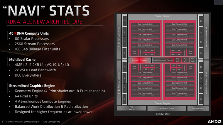
base (hmhm why 1.6GHz?) and 3.2GHz boost. Additionaly, it contsins Navi LITE GPU clocked at 1.8TF. Navi Lite? 36CUs @ 1.8GHz - 8.3TF, even that would barely make it into console IMO.

So 36CU Navi and Zen2 would not make it terribly big chip on 7nm, but along with PCB leak from Reddit which mentions 256 bit bus and 316mm² size it would make complete sense to be Sonys SOC.

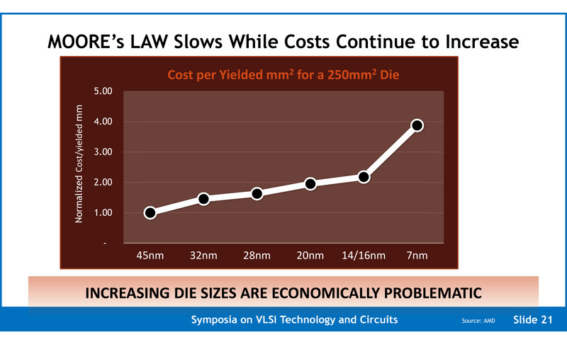
Sony has, btw, been on "roll" of sizing down their chips since PS2, which was 510mm² chip. Then came PS3 with 470mm², PS4 with 348mm² and in the end Pro with 320mm².

So as nodes get smaller and smaller, and prices for mm² get higher, Sony puts smaller die sizes in their consoles, likely duo to increased costs.

So, for me, nothing bar Gonzalo and Reddit PCB, technically speaking, makes any sense. If Sony had 13TF GPU in PS5 you would be hearing about it the minute they went to Wired and releaved PS5. Instead you have Cerny talking about immersion, 3D sound, SSD, CPU and RT. Nothing about mythical GPU (and rest assured, that Navi 13TF would be biblical. Probably matching 2080TI.
 

R600

Banned
Not to mention 12.9TF of GCN equals 10.3TF (56CU @1440MHz) of RDNA going by AMDs 1.25 IPC
So if you wanna speculate/theorize the 12.9TF being from Vega Dev kits. 8-9tf is not even close to the mark
According to AMD, Navi 9.75TF outperforms Vega56 with 10.5TF by ~31% on avg (from 25 to 40%). You are also leaving out RT hardware that will have to be emulated, so no, it fits very well actually
 

THE:MILKMAN

Member
where is it from? hard to interpret without context


R600

Banned
Thanks. This is my entire point, and this is why Navi Lite @ 1.8GHZ from Gonzalo leak makes sense. Because costs per mm² are getting higher and higher, and Sony ditched UHD from PS4Pro to make it 399$ even though die itself was smaller then PS4s.

So, on even more expensive process, with 2xRAM (more expensive one at that) and 1TB SSD, we should expect 400mm² chips? Nope.
 
Last edited:

Darius87

Member
PS2 CPU 240mm² + GPU 279mm² = 519
PS3 CPU 235mm² + GPU 258mm² = 493
PS4 APU = 348mm²
PS5 = 315mm² ?
as you can see 519 > 493 > 348 > 315 seems inline yours 380-390 seems off.

Xbox CPU 90mm² + GPU 128mm² = 218
Xbox 360 CPU 176mm² + GPU 182mm² = 358
Xbox one APU 363
Scarlet = 380-390mm²?
odd thing but for xbox actually increases 218 < 358 < 363 < my prediction 385 yours 380-390 seems inline.

Me poking fun/taking a shot at something doesn't need an audience
it does because i don't know that i don't get a joke? or you're terrible joker?

Except PS4/XB real leaks were spec leaks
more then a year before launch?
 

SonGoku

Member
I think this just tell us what we already know: 7nm yields are poor which is why AMD release small navi chips first. As yields increase costs go down
That slide is from 2017 btw
Because costs per mm² are getting higher and higher,
Yet Scarlett is 385 mm2
 
If Sony had 13TF GPU in PS5 you would be hearing about it the minute they went to Wired and releaved PS5.

Not necessarily.

MS/insiders have played the power/performance leader angle from way back when.

What is more valuable from a marketing perspective?
  1. Immediately announce killer specs that halts the opposition's current marketing strategy, allowing them to regroup and refocus their efforts elsewhere in time for release.
  2. Let the opposition continue digging their own hole with "performance leader" and then crush those numbers much closer to release.

Option 1 gives the opponent time to regroup and focus on another USP.
Option 2 deals a killing blow if the opponent's USP is performance.

Sony have been quiet, haven't they?
 
Last edited:

Ovech-King

Gold Member
Sony should be the one calling their console Anaconda .. lol. They wait in the shadows , leaving Microsoft doing their conference, even showing their Samsung chips part number ... The Japanese snek can do whatever he want to adjust its final specs... The "Anaconda" is waiting to strike (imagine those sentences spoken with the planet earth narrator voice :messenger_tears_of_joy: )
 

R600

Banned
Not necessarily.

MS/insiders have played the power/performance leader play from way back when.

What is more valuable from a marketing perspective?
  1. Immediately announce killer specs that halts the opposition's current marketing strategy, allowing them to regroup and refocus their efforts elsewhere in time for release.
  2. Let the opposition continue digging their own hole with "performance leader" and then crush those numbers much closer to release.

Option 1 gives the opponent time to regroup and focus on another USP.
Option 2 deals a killing blow if the opponent's USP is performance.

Sony have been quiet, haven't they?
I want you to completely remove PR speak and random leakers that know everything from number of CUs and clockspeeds to launch titles, and concentrate on 2 things.

1. 100% legit, known technical leak - Gonzalo.

1.1 Gonzalo is a console SOC
1.2 Gonzalo is connected to Ariel codename, found in PCI ID base under Sonys chips.
1.3 Has base Zen2 clocks of 1.6GHZ and boost of 3.2GHZ
1.4 Was QS sample in April
1.5 Has Navi 10 LITE chip on board - clocked at 1.8GHZ (was 1GHZ in January - ES1)
1.6 Ties up very well with another leak (or fantastic fake) - Reddit PS5 Dev Kit PCB leak from OQA (outgoing quality assurance

2. Navi 10 arch and technical properties such as TDP and die size


After you do so, come back to me and tell me how in the hell can anyone with 1 gram of brain think 13TF Navi with RT hardware, Zen2 and 24GB of RAM (880 GB/s at that) fit in console box. Ill wait.
 

SonGoku

Member
as you can see 519 > 493 > 348 > 315 seems inline yours 380-390 seems off.
PlayStation and Xbox took similar approaches this gen, trying to set a pattern under different circumstances never works.
Unlike past node transitions, 7nm has more density increase improvements than power reductions. To exploit the nodes strength you need a big chip
it does because i don't know that i don't get a joke? or you're terrible joker?
PS5 315mm2 vs XB 390 mm2 is as ridiculous a claim as 7nm EUV PS5 vs 7nm XB
Thats the joke, couldn't care less whether you find it funny or not, not here to entertain you :)
more then a year before launch?
I think so, not sure though
 
Last edited:

R600

Banned
Mind you Scarlett chip at min is 338mm². Its no where near conclusive to say its 380-400mm². It can EASILY be smaller then Scorpio, very thin margins if you are trying to get die size from that video.

And if its on smaller size with wider bus, then die sizes could be much much closer as far as actual CUs and cores go.
 
Last edited:
1. We have to distinguish if guy leaking this is dev
2. After that we have to see if 56 @ 1.8GHz - 13TF chip is referring to final spec or actual dev kits that went out with PC hardware (this would be analogue to PS4 dev kit roadmap where in June 2012 first PC based dev kits went out - see here http://vgleaks.com/orbis-devkits-roadmaptypes/)
3. Sony and MS gave target specs to devs back in 2012, but not official documentation. But with Pro and X, this happened much later. For X, dev kits were sent less then a year console went out.
4. You have to ask yourself validity of a leak that says 13TF Navi @ 1.8GHz can be expected in console, because EVERYTHING we know about Navi tells us we shouldnt expect anything close.
5. Why 1.8GHz? In April, 1.8GHz Gonzalo was leaked. Its ID decoded tells us its console SOC, connected to codename Ariel found amongst Sony's chips in PCI ID base.

Just to jump back to earlier points...
  1. We have to assume the person leaking this is a developer. If it is a fake leak, the real info will be stronger. You don't fake leak your actual values if you want to mislead the competition.
  2. Final spec. Developers need to know what the release target is, not the dev environment. This influences everything from concept, design through to implementation, release and beyond.
  3. No idea about this, I can't comment.
  4. We're looking at early Navi so far. A first iteration to get stuff out to market asap to recoup costs. Incrementally sell from the low end upwards, possibly becoming the flagship gaming cards if big navi et al perform as expected.
  5. Because if not a developer, it is a fake leak. Dropped intentionally to mislead with a lower target. The leak didn't get much traction, then images of the dev summit were attached to add credibility. Ask yourself, who takes random ass photos at a dev summit?
At worst, these are actual specs leaked by a dev. If it's a dev leaking, where are all the other dev leaks?

At best the croissant leak is a fake and the real specs are higher still.
 
Last edited:

SonGoku

Member
Mind you Scarlett chip at min is 338mm². Its no where near conclusive to say its 380-400mm². It can EASILY be smaller then Scorpio, very thin margins if you are trying to get die size from that video.

And if its on smaller size with wider bus, then die sizes could be much much closer as far as actual CUs and cores go.
Calculations point towards 380-390
Logic points towards 380-390
The slide posted here is from 2017, thats 3 years from launch. As yields go up, costs go down. With 6nm available soon after launch, quick costs reductions are possible
. If Sony had 13TF GPU in PS5 you would be hearing about it the minute they went to Wired and releaved PS5
Announcing hard numbers subject to change is a PR nightmare waiting to happen, let alone before a formal reveal
 

R600

Banned
For 13TF to be true you have to jump through dozens of hoops we have 0 evidence will ever happen.

To understand we are well below 10TF is to listen to Cerny or Phil talk about next gen consoles.

"Immerssion...CPU simulations...3D sound...propriatary SSD for amazing loading...hardware RT"

Not one line about this biblical GPUs you guys are expecting. I was here in 2012. Know what folks expected? 2.5-3TF machines. Why? Because EPIC had hard on on "2TF is minimum for next gen, we are urging Sony/MS to listen".

What happened? We got 1.2TF Xbox and 1.8TF PS4. Both well below expected, Xbox embarassingly so (back then 4TF was highest rated GPU)
 
Last edited:

SlimySnake

Flashless at the Golden Globes
Thanks. This is my entire point, and this is why Navi Lite @ 1.8GHZ from Gonzalo leak makes sense. Because costs per mm² are getting higher and higher, and Sony ditched UHD from PS4Pro to make it 399$ even though die itself was smaller then PS4s.

So, on even more expensive process, with 2xRAM (more expensive one at that) and 1TB SSD, we should expect 400mm² chips? Nope.
Arent you expecting a $499 console though? Navi Lite makes sense to me for a $399 console. But i think with SSD and ray tracing, its pretty clear they will be going for a premium price.

The PS4 APU cost them $100 in a console that had a BOM of $381. If the BOM for the PS5 is $481, they can easily afford to have an APU 50% more expensive this time around and have an additional $50 to spend towards vapor chamber cooling, and any extra costs for SSDs and UHD over the standard HDD and Bluray drives they had back in 2013.
 

R600

Banned
Arent you expecting a $499 console though? Navi Lite makes sense to me for a $399 console. But i think with SSD and ray tracing, its pretty clear they will be going for a premium price.

The PS4 APU cost them $100 in a console that had a BOM of $381. If the BOM for the PS5 is $481, they can easily afford to have an APU 50% more expensive this time around and have an additional $50 to spend towards vapor chamber cooling, and any extra costs for SSDs and UHD over the standard HDD and Bluray drives they had back in 2013.
I am firmly expecting $500. Just look at PS4Pro with 320mm² die on 16nm node. It was smaller die, but system cost more then PS4 with bigger die because cost per mm² went up with each smaller node.

Sony didnt even put in UHD because they wouldnt be able to sell it for $400.

So how do we get chip with Zen2, ~ Navi 5700, Ray Tracing, 16GB of GDDR6, UHD and 1TB of SSD for $400? We dont. And we wont.
 

SonGoku

Member
For 13TF to be true you have to jump through dozens of hoops we have 0 evidence will ever happen.
Same applies to 8-9TF estimates
For the record im not pushing the 13TF narrative, im sitting at 11TF
listen to Cerny or Phil talk about next gen consoles.
From Wired:
A true generational shift tends to include a few foundational adjustments. A console’s CPU and GPU become more powerful, able to deliver previously unattainable graphical fidelity and visual effects
 

IceManCat

Member
Not to mention 12.9TF of GCN equals 10.3TF (56CU @1440MHz) of RDNA going by AMDs 1.25 IPC
So if you wanna speculate/theorize the 12.9TF being from Vega Dev kits. 8-9tf is not even close to the mark


I thought it is 1.47 we are back to 1,25 again?
 
  • Like
Reactions: TLZ

THE:MILKMAN

Member
I think this just tell us what we already know: 7nm yields are poor which is why AMD release small navi chips first. As yields increase costs go down
That slide is from 2017 btw

Yet Scarlett is 385 mm2

I really don't think that is about yields. Yields always start poor(ish) and then improve. That article is clearly describing a new phenomenon (part of the end of Moore's Law).

This quote clearly takes account of yields:

Comparing the cost with yield taken into consideration, it can be seen that the 7 nm node swells to nearly twice the cost for the 16/14 nm process node.
 

R600

Banned
Same applies to 8-9TF estimates
For the record im not pushing the 13TF narrative, im sitting at 11TF

From Wired:
And this doesnt happen with 8-9TF Navi + RT? Because it absolutely does. If we get 11TF, let alone 13TF, that would be bigger jump then last gens, and as graphics tech goes forward, each new step is smaller and smaller and more expensive on top of that.

We are also having problem of mid gen refreshes that happened ~2yrs ago and we are looking for 5-6x jumps compared to them, and not to base consoles which should be the real metric.
 
After you do so, come back to me and tell me how in the hell can anyone with 1 gram of brain think 13TF Navi with RT hardware, Zen2 and 24GB of RAM (880 GB/s at that) fit in console box. Ill wait.

Maybe the real secret sauce is just a bigger power supply and better cooling with a hefty launch subsidy? ;)

Not all companies are going to have the same resources, approach and limitations.

Different constraints can breed unique solutions to the same problem.
 

SonGoku

Member
I really don't think that is about yields. Yields always start poor(ish) and then improve. That article is clearly describing a new phenomenon (part of the end of Moore's Law).

This quote clearly takes account of yields:
The graph is literally: Cost per yielded mm2
Yield is 100% the main culprit behind cost
 

R600

Banned
Using official AMD estimates

PlayStation 4: ($381 BoM / $399)
PlayStation 4 Pro: ($318 BoM / $399)
Sorry, should have specified as SOC. I think additional memory in PS4 skewed this one, as GDDR5 in those amounts where very expensive back then.

I am interested in SOC difference between the two, as OG PS4 has 10% bigger die size.
 

SlimySnake

Flashless at the Golden Globes
I am firmly expecting $500. Just look at PS4Pro with 320mm² die on 16nm node. It was smaller die, but system cost more then PS4 with bigger die because cost per mm² went up with each smaller node.

Sony didnt even put in UHD because they wouldnt be able to sell it for $400.

So how do we get chip with Zen2, ~ Navi 5700, Ray Tracing, 16GB of GDDR6, UHD and 1TB of SSD for $400? We dont. And we wont.
it cost the same though. the console was likely sold for profit.

i think MS showed you could have a 350mm2 16nm die for $499 and im pretty sure they sold it for a profit too.

I really dont think looking at the PS4/x1 gen is a good barometer to see what we will get next gen. Sony went with standard cooling and a $381 BOM. It's looking very likely they will go for $499 this gen and with MS keeping them on their toes will likely take a bigger loss than they did last gen.

Sony was using a 20 CU HD 7870 GPU with 2 disabled CUs clocked at only 800 Mhz. The full 20 CU desktop version was clocked at 1000 Mhz and 2.5 tflops. Sony couldve included vapor chamber cooling for a $10-20 extra over standard fan cooling and increased the clockspeeds to 1000mhz to get a console well over 2 tflops without increasing the APU size. So even back then, they could have had a powerful console if they were willing to take a bigger loss.

This time around they have an extra $100 to play with.
 

SonGoku

Member
And this doesnt happen with 8-9TF Navi + RT? Because it absolutely does.
Regardless of it happening or not your thesis as to why 10TF+ is not happening is wrong which is why i posted the quote
Cerny interview doesnt support your thesis.
If we get 11TF, let alone 13TF, that would be bigger jump then last gens
Looking at peak floating point perfomance alone this gen jump was 8x
11TF vs 1.8TF is a 6x jump
 

R600

Banned
The graph is literally: Cost per yielded mm2
Yield is 100% the main culprit behind cost
Its not only yields, there is clear pattern of each new node being more expensive one.


Apparently Sony got that memo as well since their chip die sizes are following this trend, backwards.
 

THE:MILKMAN

Member
so what are you arguing then? :unsure:

I'm not arguing anything. The article I posted is saying, leaving aside yields, that a 250mm^2 chip costs twice as much as the previous node. This puts huge pressure on the console makers to limit as much as possible the size of their SoCs

At least that is my running logic here.
 

SonGoku

Member
Its not only yields, there is clear pattern of each new node being more expensive one.
For designing a chip yes but when talking about cost per mm2, yields are the number one factor
Apparently Sony got that memo as well since their chip die sizes are following this trend, backwards.
If you refer to the Pro, they had a goal in mind and they met it. The Pro is likely never udergoing a shrink so it makes sense to make the chip as small as possible. Thats not the case with PS5
 

R600

Banned
Looking at peak floating point perfomance alone this gen jump was 8x
11TF vs 1.8TF is a 6x jump
And now look how entire graphics sector has moved from 2005 to 2013 in terms of FLOPS (0.2 to ~4) and from 2013 to 2020 (4 to ~ 14) and you will notice that :

A) FLOP increase has slow down considerably
B) Prices of GPUs have gone dramatically upwards
C) Node shrinking has become harder and more expensive

So no, we should not be expecting 11-13TF because there is a chip in PC out in 2w that is rated 225W with 9.75TF. A TDP rating that consoles have NEVER matched in closed box, so why start now when everything is more expensive and complex?
 

ethomaz

Banned
Interesting. Does that mean that 1 RDNA Dual CU does double the work of a Vega CU?
Well 1 DCU is 2CUs... so yes it does the work of 2 CUs.
They just combined two CUs to use the same cache... the CUs are actually the same yet with 64 Shaders.
 
Status
Not open for further replies.
Top Bottom