Nhranaghacon
Banned
This is going to provide such a huge step up from current hardware it can not be understated.
And then the article goes on to do just that, the correct amount of stepping up this would ensure is 15-20x more complexity than anything available - particularly when ML is utilized to help the process along.
We are talking about, at 3nm - laying silicon at a level far below what the human eye can possibly see. Essentially moving around atom's to create molecular fabric waferchips.
 www.pcgamer.com
And then the article goes on to do just that, the correct amount of stepping up this would ensure is 15-20x more complexity than anything available - particularly when ML is utilized to help the process along.
We are talking about, at 3nm - laying silicon at a level far below what the human eye can possibly see. Essentially moving around atom's to create molecular fabric waferchips.
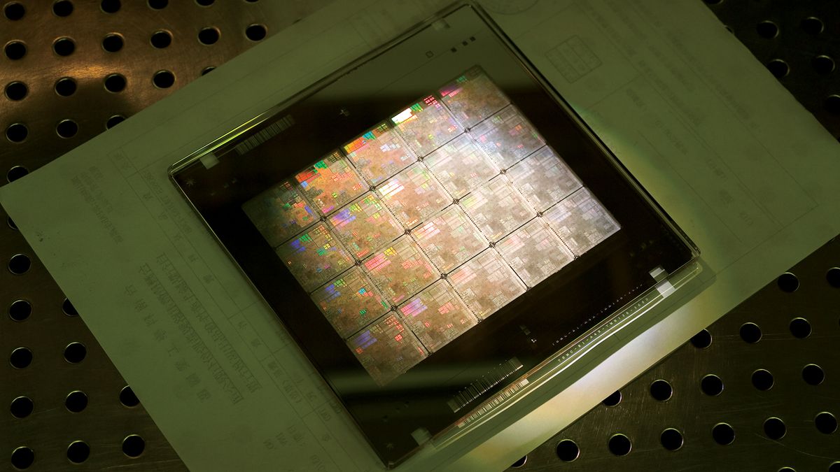
TSMC confirms 3nm tech for 2022, could enable epic 80 billion transistor GPUs
But probably a bit later than 2022...
Monster chip foundry TSMC has confirmed its 3nm production node is on track for full mass production in the second half of 2022, according to Chinese tech site ItHome (in Chinese). TSMC reckons its 3nm node will pack in somewhere north of 250 million transistors per square millimetre of silicon, making it at least two and half times more dense than Intel’s latest 10nm node. In theory, TSMC’s 3nm tech could enable a GPU three times more complex than AMD’s new Radeon RX 6000 Series chips.