

• Hey Guest. Check out your NeoGAF Wrapped 2025 results here!

How do they design the inside of computer chips?

Status
Not open for further replies.

nkarafo

Member
This is a site with some amazing high-res pictures of the insides of various older computer chips:

http://www.visual6502.org/

Just look at the 68000 CPU (the one used in Genesis/MegaDrive and many more 16bit systems)

http://www.visual6502.org/images/pages/Motorola_68000.html

In the big pics, you can clearly see each individual transistor. Keep in mind that these pictures can reach 10.000 x 10.000 resolution or more and 200+ MB, so don't do this in your old smartphone or netbook or something... i suggest looking at the lower res 20MB pictures, they work well too.

http://www.visual6502.org/images/68000/Motorola_68000_die_20x_1c_noMetal_6500w.jpg


Looking at the 68000 picture i see a very complex design, like a huge metropolis of some sort, with wiring and more than 60k individual transistors. I assume that they didn't just throw the transistors in there randomly. So each one of them was put there by someone, right? All these paths and patterns are thought out and "handcrafted" correct? If so, how many man hours would a team of people need to design something like this?

But my real question is this: Let alone the 68000 processor. This is ancient tech. What about modern processors? These have BILLIONS yes, Billions of transistors inside them. Again, i assume that they didn't throw them in the chip at random. They have to be put in some kind of order right?

Now i'm not very good at math but i think that even if you try to count to 1 billion, it will take you about 30 years (assuming you count 1 each second). Now imagine trying to place 1 billion transistors in a design. One by one. I assume it would take you several lives, more than 100 actually. Obviously, you need people to help you. But even if you had 100 men painstakingly placing the transistors 1 by 1 in a design, it would still take hundreds of years.

So how does that work. I can't warp my mind around this, someone has to design all these patterns in microscopic levels so that it can work in some mysterious way. It looks completely magic or at least alien to me.
 
My question isn't how a transistor works but how do they pack billions of them, in a thought out pattern since each one has to be in the correct place and not somewhere random. It's not a few thousands of them. It's billions of them. How can someone even draw a design with 1+ billion points on it. It's physically impossible, unless there is an automated system that helps them without being randomly generated.
 
My question isn't how a transistor works but how do they pack billions of them, in a thought out pattern since each one has to be in the correct place and not somewhere random.

Engineers use software to do that. They don't actually place billions of transistors by hand ;) Then they simulate the CPU with big server farms. If everything works correct they design the masks etc.


Also there are hundreds of people who work on the chip design. So some of them only work on the cache while other do the actual CPU cores and so on.
 
Most chips are designed in sections, each section connects to another. For example on something like a GPU you have a section dealing with shaders then you have another section dealing with video output then another to access memory etc. It takes years of design work to create a new chip design and that's why most "new chips" aren't that new but they are refinements and improvements over previous chips. Entirely new architecture is hugely expensive to create and sometimes comes out less than perfect (AMD's phenom 1 is a perfect example of messing things up the first time but then improving on it massively the second time with the phenom 2).
All design is now done on computer and the chips can be simulated in just how the work as real silicon. This negates serious design flaws. Think of it like a jigsaw puzzle. You have lots of separate pieces and then then put them together and see if it's correct.
 
Engineers use software to do that. They don't actually place billions of transistors by hand ;) Then they simulate the CPU with big server farms. If everything works without correct etc. they design the masks etc.

I want a bespoke handmade CPU.
 
I'd like to know how we got from the early CPUs to where we are today (dyes on silicon, lasers, molten copper). It seems like such a huge step. Couldn't find any documentaries on that transition.
 
Engineers use software to do that. They don't actually place billions of transistors by hand ;) Then they simulate the CPU with big server farms. If everything works without correct etc. they design the masks etc.
That software also designs the patterns right? Because it's not about placing the transistors in the chip, its also about someone drawing the actual design.

I mean, even the 68000 needs a huge resolution picture to see the transistors, imagine a modern GPU chip that has several billion transistors, it would need a drawing space as big as a continent or something, let alone actually drawing on it a design with wiring, paths, etc.
 
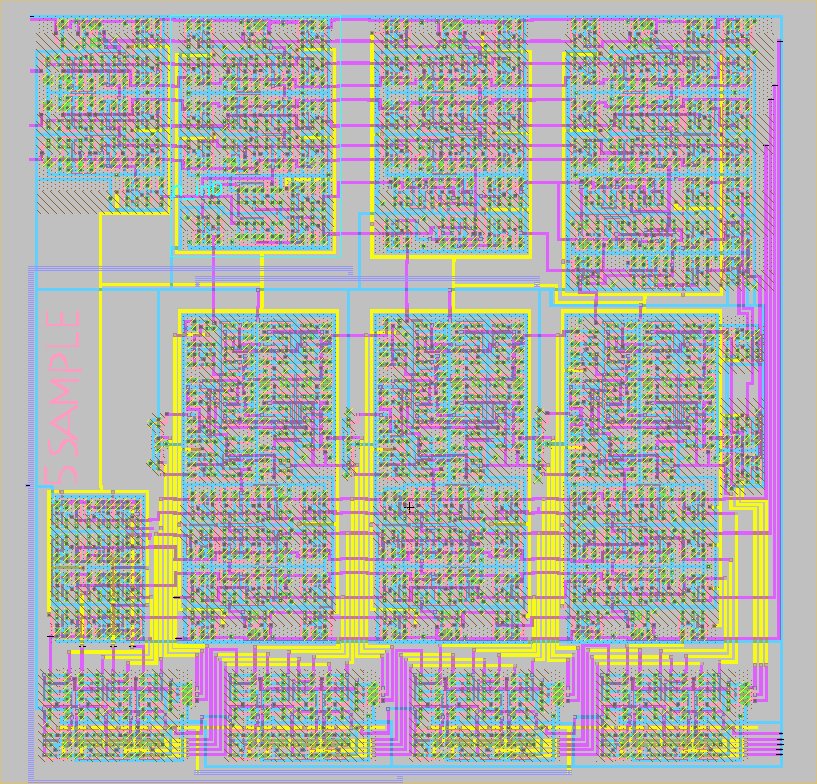
They use automated placement and routing software that handles it. I've done it in college. Even got it fabricated on some ancient process. It ran at some low MHz. But some smaller performance critical blocks are still hand optimized. You draw transistors substrates and gates and metal wire layers etc in the layout editor just like an architect draws buildings in autocad.
 
I'd like to know how we got from the early CPUs to where we are today (dyes on silicon, lasers, molten copper). It seems like such a huge step. Couldn't find any documentaries on that transition.
51dSmWMygBL._SY344_BO1,204,203,200_.jpg
 
To me your question is not very clear. There are of course different levels of abstractions, and depending on the project you can choose the most appropriate to work with. The scale of the project and its requirements also have an influence on the tool used. Sometimes you use cad programs, sometimes you sinthesize the components by passing the requirements of the component itself (what it is supposed to do, namely the truth table) to "compilers" like espresso. Sometime you draw the entire project by hand, starting from the logic gates (like the great Italian Physicist Federico Faggin did for the amazing Z80), sometimes you let software do the optimizations. In the past it was usual to draw maps (the so called Karnaugh maps) the size of a table to manually minimize through an algorithm the number of logic elements, and thus transistors, needed for your project. Nowadays it's a whole different story.
 
That software also designs the patterns right? Because it's not about placing the transistors in the chip, its also about someone drawing the actual design.

Yeah the software calculates the best conductor tracks etc.

Something like this, but a million times bigger:
UG_median_filter.jpg


The enginners just "tell the software" how they want it to have.

And by "just tell the software" I mean hundreds of people with master degrees over the span of 4 or 5 years.
 
We design the RTL in a language called Verilog, which is all the logic but not where everything is placed, and then the physical guys lay it out and figure out where everything goes. Some things in the actual design are put in to help the physical guys jobs easier, but most of everything we do is logic/timing/power.
 
To me your question is not very clear.
Well, basically it comes down to this.

a Chip works in a specific way. That means an intelligence actually designed it. All those paths the wiring and the transistor placement could not be randomly generated. Someone has to draw and inspect the design. This sounds doable in older chips that had thousand of transistors to draw but impossible after you reach astronomical numbers like hundreds of millions or billions.

So yeah, automated software and computers help in this obviously. But it's still amazing how a design like these pictures in the OP can exist in a tiny space but being hundreds of thousands of times more dense and still work as it should... i mean what if i was to take one, just one transistor and put it in a different place. Would that ruin the whole design?


Yeah the software calculates the best conductor tracks etc.

Something like this, but a million times bigger:
UG_median_filter.jpg


The enginners just "tell the software" how they want it to have.

And by "just tell the software" I mean hundreds of people with master degrees over the span of 4 or 5 years.
Thanks, i think it starts to make a tiny bit of sense :P
 
Well, basically it comes down to this.

a Chip works in a specific way. That means an intelligence actually designed it. All those paths the wiring and the transistor placement could not be randomly generated. Someone has to draw and inspect the design. This sounds doable in older chips that had thousand of transistors to draw but impossible after you reach astronomical numbers like hundreds of millions or billions.

So yeah, automated software and computers help in this obviously. But it's still amazing how a design like these pictures in the OP can exist in a tiny space but being hundreds of thousands of times more dense and still work as it should... i mean what if i was to take one, just one transistor and put it in a different place. Would that ruin the whole design?


Thanks, i think it starts to make a tiny bit of sense :P

Yes, having a transistor in the wrong place would ruin the whole design. There are tons of bugs in hardware and often they are caused by situations that put the hardware in a very strange state that it can't recover from that wasn't seen during the design and testing phases. There are practically an infinite amount of state a cpu can have and seeing them all is impossible during this design phase.
 
We design the RTL in a language called Verilog, which is all the logic but not where everything is placed, and then the physical guys lay it out and figure out where everything goes. Some things in the actual design are put in to help the physical guys jobs easier, but most of everything we do is logic/timing/power.

fucking Verilog. So much wasted time because of a wire was wO instead of w0, or other similarly stupidly small mistakes. God damn it;l.sakjn;lsakjf;alskjhf;sadklhjf;sadlkj
 
A lot of things are standard libraries too, like logic or arithmetic units. The hard part these days is placement, gate sizes, busses, etc.

Edit: I've done FPGA work as well as stuff on Spectre.
 
fucking Verilog. So much wasted time because of a wire was wO instead of w0, or other similarly stupidly small mistakes. God damn it;l.sakjn;lsakjf;alskjhf;sadklhjf;sadlkj

As someone who does this stuff professionally, we do not like when a wire is called "wO". That tells me nothing about what the signal does and why its there. I dont like having to guess functionality :P
 
Well, basically it comes down to this.

a Chip works in a specific way. That means an intelligence actually designed it. All those paths the wiring and the transistor placement could not be randomly generated. Someone has to draw and inspect the design. This sounds doable in older chips that had thousand of transistors to draw but impossible after you reach astronomical numbers like hundreds of millions or billions.

So yeah, automated software and computers help in this obviously. But it's still amazing how a design like these pictures in the OP can exist in a tiny space but being hundreds of thousands of times more dense and still work as it should... i mean what if i was to take one, just one transistor and put it in a different place. Would that ruin the whole design?

Well, firstly keep in mind that there is a lot of repetition inside a chip. We all used to hearing about 8-bit, 16-bit, 32-bit etc. Doing, for example, a 32-bit adder is as simpe as stucking together eight 4-bit adder. The moment you design a 4-bit adder you also have a 32-bit adder for free. The design of digital electronics is very incremental. This is true on various levels. On a higher level it's important to note that elements of an architecture could be recycled in the next one. It's equally well known that modern CPUs are hindered by legacy x86 instructions hardware decoding. In addition to that you have, for example, cache of various levels, which take the larger portion of the chip. So it's not true that evereything has to been designed from scratch.

Regarding the transistor question, I believe that these chips are designed to be fault tolerant to a certain degree, but this is not a topic I'm familiar with.
 
a Chip works in a specific way. That means an intelligence actually designed it. All those paths the wiring and the transistor placement could not be randomly generated.

That's not necessarily true btw. One could theoretically (or maybe this actually happens) be designed by an evolutionary algorithm. Which is guided randomness, ie GEN 1 is randomly generated according to a set of simple rules, the ones that work the best are used as the progenitors of GEN 2 etc
 
Yes, having a transistor in the wrong place would ruin the whole design. There are tons of bugs in hardware and often they are caused by situations that put the hardware in a very strange state that it can't recover from that wasn't seen during the design and testing phases. There are practically an infinite amount of state a cpu can have and seeing them all is impossible during this design phase.
This is fascinating.

And even more fascinating is how i find old systems (like pentium 4) in the garbage or recycle bins. That chip you throw away has an impossible complex part inside it. One that you can't even make out with the strongest microscopes. This invisible to the naked eye thing, that thing is incredibly complex and incredibly small (down to atomic level even) yet it exists in the physical world. And it works somehow. And you throw it away like it's nothing.

Mass production of incredible technology is fascinating.
 
This is fascinating.

And even more fascinating is how i find old systems (like pentium 4) in the garbage or recycle bins. That chip you throw away has an impossible complex part inside it. One that you can't even make out with the strongest microscopes. This invisible to the naked eye thing, that thing is incredibly complex and incredibly small (down to atomic level even) yet it exists in the physical world. And it works somehow. And you throw it away like it's nothing.

Mass production of incredible technology is fascinating.

The pentium 4 is in the garbage bin because it's branch misprediction penalty for having such a deep pipe was high, among several other assumptions that were made about its technology that didn't pan out. They essentially threw away it's arch and went onto something else.
 
I took a course on this in 4th year of undergrad, called VLSI Systems, over 10 years ago. The lab assignments involved doing hand-drawn layouts of each individual element of a 4-bit CPU in a layout program. After you create each basic element and run timing simulations on it to make sure it works properly, you move on to larger elements that group together multiple units of the smaller building blocks. So you start by drawing a transistor (similar to drawing pixel by pixel in Photoshop), then you build all of the different logic gates you need like NAND and NOR gates or whatever, by laying out multiple transistors in a precise arrangement (e.g. copy/paste the transistor you drew).

There are rules to how close particular metal layers can be positioned next to other layers as electrical signals in one material can impact other materials that are too close, or arranged in certain ways. After you make your logic gates, you can then start making different data/processing units by combining arrangements of the logic gates. Spend enough time doing this and you ultimately can make a whole CPU. As there are space limitations and performance goals, you may determine that your layout is not optimal, and you may need to tweak various elements by either repositioning transistors, or tweaking the gate or transistor layout. In some cases, you might end up customizing particular transistors or gates to fit where you need them, so that each transistor in the CPU might not end up looking precisely identical. It's actually pretty fun. There's kind of an art to it.

If you were building a modern CPU, you wouldn't do all of this by yourself. A 4-bit CPU took me a long time. A modern 64-bit CPU is not a one person job. There would probably be a team of people working on each individual processing unit, and another team of people working purely on designing the most compact, fastest transistors and logic gates possible. Another group would probably be testing the whole thing once it's all linked together.
 
As has been already said. This complexity is divided in several layers of abstraction. Transistor level design is more the realm of materials scientists and physicists I think while the functional design of the behaviour of these circuits is done by engineers via using hardware description languages (HDL) similar to programming languages but for hardware. This is usually done at the Register transfer level (RTL) utilising several programming constructs as found in other high level languages but still dealing with a much lower level of abstraction. The synthesis from this 'code' to logic gates is automated via software which optimises the circuit according to various parameters (timing, number of gates etc). Before creating a circuit an architecture is described for the processor (which also occurs at different levels) but most obvious I can think off is defining the instruction set, the set of operations which the processor should be able to perform. Outside of this then issues of pipelining, scheduling etc arise which is sometimes said to be the micro architecture (I think). This is obviously a simplification of the actual process but gives a rough idea.
 
As has been already said. This is complexity is divided in several layers of abstraction. Transistor level design is more the realm of materials scientists and physicists I think while the functional design of the behaviour of these circuits is done by engineers via using hardware description languages (HDL) similar to programming languages but for hardware. This is usually done at the Register transfer level (RTL) utilising several programming constructs as found in other high level languages but still dealing with a much lower level of abstraction. The synthesis from this 'code' to logic gates is automated via software which optimises the circuit according to various parameters (timing, number of gates etc). Before creating a circuit an architecture is described for the processor (which also occurs at different levels) but most obvious I can think off is defining the instruction set, the set of operations which the processor should be able to perform. Outside of this then issues of pipelining, scheduling etc arise which is sometimes said to be the micro architecture (I think). This is obviously a simplification of the actual process but gives a rough idea.

This is a good simplification. I think people don't know how complicated and how many people are required to make the CPU in their phones. There's a reason they cost upwards of 700 dollars.
 
As someone who does this stuff professionally, we do not like when a wire is called "wO". That tells me nothing about what the signal does and why its there. I dont like having to guess functionality :P

yeah yeah, this was only like designing carryskip adders for 32 bits or something for a school project, or at biggest designing a Floating Point Unit. I imagine there's a lot better design patterns out there than me doing it at midnight improvising whilst downing a pot of coffee.
 
yeah yeah, this was only like designing carryskip adders for 32 bits or something for a school project, or at biggest designing a Floating Point Unit. I imagine there's a lot better design patterns out there than me doing it at midnight improvising whilst downing a pot of coffee.

I know it was, I was just giving you some undue grief ;)
 
I've just started doing layouts for basic logic gates. Here are a couple I've made:

Inverter schematic:

e6njEEK.png


Inverter layout:

81xpXHw.png


3-input NAND schematic:
bLHorUp.png


3-input NAND layout (with transistor folding):
00HGwj8.png


The schematics are the easy part to make. They just define how the gates will function. The layouts are where you actually define where the individual materials (metal, polysilicon, contacts, diffusion, etc...) will reside. There are all sorts of rules as far as what can go where in these layouts (called "standard cell" rules), and the software checks that you're observing these rules correctly. The rules basically ensure that you can then take these gates and integrate them into a much larger circuit easily.
 
OP, at today sizes, you use VHDL or Verilog to program the logic and then you fight with Cadence Virtuoso to accept it.

fucking Verilog. So much wasted time because of a wire was wO instead of w0, or other similarly stupidly small mistakes. God damn it;l.sakjn;lsakjf;alskjhf;sadklhjf;sadlkj

I prefer VHDL

I don't like either lol

Looks like the game froze. Someone blow into the NES cartridge.

LOL

I've just started doing layouts for basic logic gates. Here are a couple I've made:

Inverter schematic:

e6njEEK.png


Inverter layout:

81xpXHw.png


3-input NAND schematic:
bLHorUp.png


3-input NAND layout (with transistor folding):
00HGwj8.png


The schematics are the easy part to make. They just define how the gates will function. The layouts are where you actually define where the individual materials (metal, polysilicon, contacts, diffusion, etc...) will reside. There are all sorts of rules as far as what can go where in these layouts (called "standard cell" rules), and the software checks that you're observing these rules correctly. The rules basically ensure that you can then take these gates and integrate them into a much larger circuit easily.
Awww, Cadence pictures.

I remember one of the projects at school was designing and simulating sub threshold CMOS logic. Fun.

BTW, you're wasting space and the taps are too big.
 
What I find amazing about the manufacture of ICs is that we've moved to such a small lithography process that the components are mere atoms in length and width.
 
What I find amazing about the manufacture of ICs is that we've moved to such a small lithography process that the components are mere atoms in length and width.
That's not the most impressive thing. The fact that the thing works at all with the linear models we use to design it is really impressive.

It is an art. And noise analysis almost seems pseudo science due to the approximations, yet it works!
 
Aside from the well taps, how could I save space? We're only allowed to use vertical polys. I literally just started so I don't know this stuff.
There is way more than I would be able to cover.

Go to your college library and check out "CMOS VLSI Design: A Circuits and Systems Perspective" by Weste and Harris.

Either the 4th or 3rd edition works, whichever they have.

Amazon link for reference http://www.amazon.com/dp/0321547748/?tag=neogaf0e-20

Not only the book explains it very well, inside the covers there are layouts so you can see how optimized stuff looks like for NANDs, NORs, Flops, MUX, Full Adder and others. At least the 4th edition has them.

That's the book I used for both the undergraduate and graduate digital CMOS design class. For analog there is another book by Razavi but I don't remember the name at the moment.
 
There is way more than I would be able to cover.

Go to your college library and check out "CMOS VLSI Design: A Circuits and Systems Perspective" by Weste and Harris.

Either the 4th or 3rd edition works, whichever they have.

Amazon link for reference http://www.amazon.com/dp/0321547748/?tag=neogaf0e-20

Not only the book explains it very well, inside the covers there are layouts so you can see how optimized stuff looks like for NANDs, NORs, Flops, MUX, Full Adder and others. At least the 4th edition has them.

I've got that book. The problem is they don't go very deep into transistor folding, so with the NAND3 I sort of had to make it up as I went.
 
I've got that book. The problem is they don't go very deep into transistor folding, so with the NAND3 I sort of had to make it up as I went.
I'll check my notes and let you know if I have anything else. It has been while.
 
0. Product managers consult with customers and engineering to decide what the goals of the new chip are going to be: lower power, support Feature X, etc.

1. A simulator is created in a high-level programming language like C++ that models the functionality and performance of a current processor. Microarchitects modify the architecture they are simulating, trying out different ideas to improve performance, power, etc. This becomes the basis for the logic design.

2. RTL designers translate the functionality of architecture into a logic description using a hardware description language (like VHDL or Verilog) that is understood by automated circuit-design tools, evaluating performance and power consumption along the way. This becomes the basis for the physical design.

2a. Depending on performance or power constraints, parts of the design may be hand-optimized by engineers designing at a transistor level.

3. Physical designers modify the output of the automated logic design tools, adjusting placement or wire routing as necessary to make sure they do not violate any constraints on electrical properties of the technology they are using and ensuring that sensitive components like clock trees or phase-locked loops are working properly.

4. The design is sent to a foundry to be fabricated. It comes back and inevitably does not work.

5. Test engineers determine why it isn't working. It gets kicked back up the stack as far as necessary to make a fix.

6. Steps 4-5 repeat until an acceptable yield rate is achieved.

I think that covers the major points, but there is a lot more testing that goes on at every phase than what I described.
 
Status
Not open for further replies.
Top Bottom