• Hey Guest. Check out your NeoGAF Wrapped 2025 results here!

How do they design the inside of computer chips?

Status
Not open for further replies.
From what I can remember from my FPGA course, NAND all the things! Let's take the FPGA as the chip example, it stands for "field programmable gate array". It is basically like a sandbox of logic chips whose connections is determined by some program that is compiled. The chips at a very basic level are probably all NAND gates. If you're not familiar with logic theory if you pass inputs through a particular gate, you get some output. These gates have different behaviors. An AND gate for example outputs true if all inputs are true, false otherwise. Similarly an OR gate outputs true if any of its inputs are true, false otherwise. NAND gates produce the opposite output of an AND gate. NANDs are also very special in that they can be combined with other NANDs to produce any other logic gate. A NOT gate for example negates the input (input=true, output=false). A NOT gate behavior can be created by taking the single input and passing it as both inputs to a NAND gate (in1=true, in2=true, in1 AND in2 = true, therefore in1 NAND in2 = false, try this with in1/in2=false). Going even deeper, a NAND logic can be created from electronic components called transistors. Basically think of a transistor as a water valve: water from a source comes into the valve, there's an output, and the valve itself which controls the flow. Same concept in electronics, you have a voltage source on one end, a voltage output on the other, and a voltage input, where if triggered, allows flow from the source to the output. I forget the exact circuit but a NAND gate is created by some combination of these transistors. And that's how you get the circuitry inside these chips.

Of course, this information is probably dated and chip design has most likely changed over the years but this is how I've always understood it.
 
From what I can remember from my FPGA course, NAND all the things! Let's take the FPGA as the chip example, it stands for "field programmable gate array". It is basically like a sandbox of logic chips whose connections is determined by some program that is compiled. The chips at a very basic level are probably all NAND gates. If you're not familiar with logic theory if you pass inputs through a particular gate, you get some output. These gates have different behaviors. An AND gate for example outputs true if all inputs are true, false otherwise. Similarly an OR gate outputs true if any of its inputs are true, false otherwise. NAND gates produce the opposite output of an AND gate. NANDs are also very special in that they can be combined with other NANDs to produce any other logic gate. A NOT gate for example negates the input (input=true, output=false). A NOT gate behavior can be created by taking the single input and passing it as both inputs to a NAND gate (in1=true, in2=true, in1 AND in2 = true, therefore in1 NAND in2 = false, try this with in1/in2=false). Going even deeper, a NAND logic can be created from electronic components called transistors. Basically think of a transistor as a water valve: water from a source comes into the valve, there's an output, and the valve itself which controls the flow. Same concept in electronics, you have a voltage source on one end, a voltage output on the other, and a voltage input, where if triggered, allows flow from the source to the output. I forget the exact circuit but a NAND gate is created by some combination of these transistors. And that's how you get the circuitry inside these chips.

Of course, this information is probably dated and chip design has most likely changed over the years but this is how I've always understood it.

That's correct as far as field-programmable stuff goes, but most digital logic today isn't field-programmable. It would be a huge waste.
 
That's correct as far as field-programmable stuff goes, but most digital logic today isn't field-programmable.

Right, chips only need the circuitry that they're designed for (ie, not programmable) but I was simply using it as an example. Additionally they need not have to be as complex as an FPGA (why use multiple NANDs to create an AND gate when you can just use a single AND?).
 
Maybe it's because we never covered VLSI but I found analog design with transistors far more intriguing than digital transistor design. Then there's signal processing and especially RF design which are pretty challenging and fun too.
 
Maybe it's because we never covered VLSI but I found analog design with transistors far more intriguing than digital transistor design. Then there's signal processing and especially RF design which are pretty challenging and fun too.

Much more difficult too. I'm taking an analog class and a digital class side-by-side, and that analog class can go fuck off and die.

Analog is much more specialized. We only really need analog these days for analog-to-digital converters and for amplifying small signals, but those needs will never really go away.
 
I've got that book. The problem is they don't go very deep into transistor folding, so with the NAND3 I sort of had to make it up as I went.
Ok, So I checked a bit more.

1. You aren't supposed to use Metal 1 in both directions. Use it vertically and then use Metal 2 for horizontal, unless your really need to use M1.

2. To much Metal 2 in cross patterns. Why? They make the circuit look busy.

3. Use the poly only up to what's you need it. No need to extend it up to the top of if there isn't a well for it. It just adds capacitance. The M1 tap takes care of what you are trying to do.

4. There is too much wasted space on top of the PMOS. Cut that until the minimum the DRC will let you. More metal = more parasitic capacitance.

Check figures 4.17 and 4.18 and study the shared and merged contact diffusion. That's the base for folding since it helps to reduce the physical width.

Much more difficult too. I'm taking an analog class and a digital class side-by-side, and that analog class can go fuck off and die.

Analog is much more specialized. We only really need analog these days for analog-to-digital converters and for amplifying small signals, but those needs will never really go away.
Check subthreshold digital logic and you'll see why you need analog design.
 
Much more difficult too. I'm taking an analog class and a digital class side-by-side, and that analog class can go fuck off and die.

Analog is much more specialized. We only really need analog these days for analog-to-digital converters and for amplifying small signals, but those needs will never really go away.

I did the same in college and bode plots in particular can DIAF. I appreciated analog design much more when we actually started building shit. I hated learning Fourier/Laplace transforms and series translations and all that but when it came down to trying to figure out how to extract an information signal from a carrier signal it all started making more sense. GPS signals are a perfect example of the need for analog to digital converters.
 
I took a VLSI (Very Large Scale Integration) course in college. I seem to recall getting an A in it but sadly my very final project didn't work perfectly -- it got complicated near the end and we were nowhere near microchips.

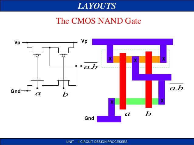
It was neat though. You start out by drawing semiconductor layers with multicolored lines in software, like people have been talking about. For example, take a very simple logic gate, an inverter from some slides on Google (software might look more complicated than this, but it should be a reasonable representation):

vlsi-stick-daigram-jcvqzzw.jpg


The left is the circuit diagram, and the right is the semiconductor layout. If x == 0, the top transistor activates, connecting 1 to the output. If x == 1, the bottom transistor activates, connecting 0 to the output. In both cases the input is inverted, so it's a working inverter.

Now, you see the input and output lines on the big colored line drawing? Imagine you have another gate that shares the same V_DD and Gnd lines, and you want to connect them together. Here's a NAND gate:

vlsi-stick-daigram-jcchk3d.jpg


You could feed that blue/purple output line from the NAND gate into the inverter above, making a more complicated drawing that's all connected together. In my class, we were given assignments throughout the semester where we would build more and more complicated circuits, connecting them together. Eventually, maybe you've built a 1-bit memory cell. Maybe you can store each thing you build as some sort of "building block" so you don't have to redesign it each time.

What if you want to make a full 32-bit (or 64-bit) memory cell at the end of the semester? Well, instead of designing it by hand, you can pull a bunch of the 1-bit blocks you already designed and link them together. Eventually you ended up with a massive complicated-looking block that you designed every part of, which was really cool...except for mine not perfectly working because I didn't get it all properly figured out in time. :P
 
Maybe it's because we never covered VLSI but I found analog design with transistors far more intriguing than digital transistor design. Then there's signal processing and especially RF design which are pretty challenging and fun too.
One of my professors used to say: "Analog designs only have two elements: Current mirrors and differential pairs. And one is a special case of the other."

If you dominate them, you'll do fine.
 
Ok, So I checked a bit more.

1. You aren't supposed to use Metal 1 in both directions. Use it vertically and then use Metal 2 for horizontal, unless your really need to use M1.

2. To much Metal 2 in cross patterns. Why? They make the circuit look busy.

3. Use the poly only up to what's you need it. No need to extend it up to the top of if there isn't a well for it. It just adds capacitance. The M1 tap takes care of what you are trying to do.

4. There is too much wasted space on top of the PMOS. Cut that until the minimum the DRC will let you. More metal = more parasitic capacitance.

Check figures 4.17 and 4.18 and study the shared and merged contact diffusion. That's the base for folding since it helps to reduce the physical width.


Check subthreshold digital logic and you'll see why you need analog design.

Thanks for the response. I think a lot of this is stuff that the professor dictated in order to make it easier to grade:

1. we were told to only use metal 1

2) the metal 2 horizontal strips are actually just there to dictate where I can place the inputs and outputs. Metal 2 gets deleted before submission

3) we're told to space poly 0.05 um from the PR boundary in the vertical direction

4) Our P implant region height is also set (PIMP)

So yeah, within the (possibly arbitrary) rules they set, I'm not sure what else I could do. Thanks though!
 
Man, getting flashbacks to my VLSI class and the ridiculous number of hours that went into the final project (a MIPS processor)
 
That's not an optical microscope though, which is what he probably meant.
Oh yes, thank you.

What's the best optical microscope then? I mean how far could it go.


I think the most complex CPU i have ever seen zoomed in with an optical microscope is the PS1 CPU. The picture was so big, it had to be broken in smaller parts. Anything above that is too low res to make out the transistors. But that was a couple of years ago. Dunno if we have detailed die pics of more powerful chips now.
 
They still are in a way. They run much much faster than computer simulations (and are obviously way slower than real silicon)
The crazy thing is how the programmable logic market tries to cater to people designing large chips. But the FPGA itself needs to be much larger than the part it's simulating, and to be reasonably fast it needs to be on the newest possible process nodes. Hence you get things like Altera's Stratix series, where individual chips can be comparable in cost to a new car.

That'll put the fear of ESD into an electrical engineer (maybe)!
 
Thanks for the response. I think a lot of this is stuff that the professor dictated in order to make it easier to grade:

1. we were told to only use metal 1

2) the metal 2 horizontal strips are actually just there to dictate where I can place the inputs and outputs. Metal 2 gets deleted before submission

3) we're told to space poly 0.05 um from the PR boundary in the vertical direction

4) Our P implant region height is also set (PIMP)

So yeah, within the (possibly arbitrary) rules they set, I'm not sure what else I could do. Thanks though!

Oh. My professor actually gave us bonus points for making the most efficient layout we could lol.

I think it's more of training wheels until you're ready.

The crazy thing is how the programmable logic market tries to cater to people designing large chips. But the FPGA itself needs to be much larger than the part it's simulating, and to be reasonably fast it needs to be on the newest possible process nodes. Hence you get things like Altera's Stratix series, where individual chips can be comparable in cost to a new car.

That'll put the fear of ESD into an electrical engineer (maybe)!
I remember drooling at the big FPGAs for the research projects. I loved checking Digilent to see what was new.
 

...What is Bjork on about? That poet's description and distrust of pixels/discrete elements sounds a lot like Prince's attitude towards digital music (something to the effect of all those 1s and 0s can't be good for your brain).

The crazy thing is how the programmable logic market tries to cater to people designing large chips. But the FPGA itself needs to be much larger than the part it's simulating, and to be reasonably fast it needs to be on the newest possible process nodes. Hence you get things like Altera's Stratix series, where individual chips can be comparable in cost to a new car.

That'll put the fear of ESD into an electrical engineer (maybe)!
I remember being told that some companies hire emulators because their purchase cost is in the millions. What type of hardware are emulators made from?
 
Oh yes, thank you.

What's the best optical microscope then? I mean how far could it go.


I think the most complex CPU i have ever seen zoomed in with an optical microscope is the PS1 CPU. The picture was so big, it had to be broken in smaller parts. Anything above that is too low res to make out the transistors. But that was a couple of years ago. Dunno if we have detailed die pics of more powerful chips now.

Chipworks has some die shots. Check the Wii U thread about the die shots to see what they can do. You'll have to search for it, sorry.

But the problem is that optical is limited by the light spectrum. I remember it wasn't useful for anything 400µm or smaller tech.
 
This is a good simplification. I think people don't know how complicated and how many people are required to make the CPU in their phones. There's a reason they cost upwards of 700 dollars.
The CPUs themselves cost less than 30 though :P

The prices aren't public, but I think 30 is in the ballpark for aa fairly high end SoC.
Chipworks has some die shots. Check the Wii U thread about the die shots to see what they can do. You'll have to search for it, sorry.

But the problem is that optical is limited by the light spectrum. I remember it wasn't useful for anything 400µm or smaller tech.
Nanometres. Visible light's wave length is 400-700nm so it's impossibly to see stuff smaller than that. This is also an issue for chip making because they use light to "print" them.
 
The CPUs themselves cost less than 30 though :P

The prices aren't public, but I think 30 is in the ballpark for aa fairly high end SoC.

Nanometres. Visible light's wave length is 400-700nm so it's impossibly to see stuff smaller than that. This is also an issue for chip making because they use light to "print" them.

Yes, I misspoke. I meant to say the entire phone, not just CPU.
 
Oh yes, thank you.

What's the best optical microscope then? I mean how far could it go.

Well, there are some physical limits on how well you can resolve things using light of a given wavelength. This is due to diffraction and generally speaking the limit is on the order of the wavelength. Since light has a wavelength of a few hundred nanometers this is about how well traditional microscopes can resolve objects. Now, there are some clever ways of using non-propagating (evanescent) light, which does not diffract, to image things about a hundred times smaller than that.
 
Jeez, this thread has been quite the flashback. I'm a computer engineer, but I had to take some electrical engineering classes.
Same here. I had to take a microelectronics class too where we learned about semiconductor doping and manufacturing. I wanted to do computer engineering and embedded systems so I was happy once I got past semiconductors/VLSI/VHDL and basically never had to mess with them again. :P
 
My question isn't how a transistor works but how do they pack billions of them, in a thought out pattern since each one has to be in the correct place and not somewhere random. It's not a few thousands of them. It's billions of them. How can someone even draw a design with 1+ billion points on it. It's physically impossible, unless there is an automated system that helps them without being randomly generated.

there are eda tools which can design the gate level placements of digital circuits. Digital logic gates are built using transistors.
 
My question isn't how a transistor works but how do they pack billions of them, in a thought out pattern since each one has to be in the correct place and not somewhere random. It's not a few thousands of them. It's billions of them. How can someone even draw a design with 1+ billion points on it. It's physically impossible, unless there is an automated system that helps them without being randomly generated.

You break up the design into smaller, self-contained units. So one guy might design a multiplexer and another will design an adder. And they'll both follow the same rules ("standard cell") to ensure that these pieces can fit together smoothly.

As far as actually printing these circuits, it's a highly-involved process that requires dozens of layers of different materials. It basically involves putting down layers of materials on top of another, and sometimes employing "masks" (think masking tape) so that the material will only cover certain parts of the previous layer.
 
That software also designs the patterns right? Because it's not about placing the transistors in the chip, its also about someone drawing the actual design.

I mean, even the 68000 needs a huge resolution picture to see the transistors, imagine a modern GPU chip that has several billion transistors, it would need a drawing space as big as a continent or let alone actually drawing on it a design with wiring, paths, etc.

It depends on the chip. For example a memory chip is pretty uniform.
For a CPU on the other hand, you break it down into several units, you define the interfaces between those units and then individuals can work on creating those units independently. Once that's done, you use software to optimize the layouts. You don't have to design every transistor, It's like using macros in programmation.
 
So turns out this may be my first job after graduation. I'm excited!

I thought I'd ask here, what are some good references on ASIC design and testing, RTL coding and GPU architecture (GPUs in particular as I don't know much about them outside of their SIMD structure)?
 
Much more difficult too. I'm taking an analog class and a digital class side-by-side, and that analog class can go fuck off and die.

Analog is much more specialized. We only really need analog these days for analog-to-digital converters and for amplifying small signals, but those needs will never really go away.

Don't forget things like high speed paths.

I've been working with debugging stuff with lab people at work and maaan, debugging issues related to analog stuff is a paaain compared to solely digital issues.
 
So turns out this may be my first job after graduation. I'm excited!

I thought I'd ask here, what are some good references on ASIC design and testing, RTL coding and GPU architecture (GPUs in particular as I don't know much about them outside of their SIMD structure)?
Congrats man.
I wanted too but could never get into it after graduation :(
For the first two there isn't much, but I'll look around. As for the GPUs, I've never seen much info about them. But, check out http://miaowgpu.org/ which is an open source GPU based on the AMD southern islands ISA.
 
So turns out this may be my first job after graduation. I'm excited!

I thought I'd ask here, what are some good references on ASIC design and testing, RTL coding and GPU architecture (GPUs in particular as I don't know much about them outside of their SIMD structure)?

There are no really great references for GPU architecture, because the companies do not publish microarchitectural details so a lot of the public information is reverse engineering and speculation. Your best bet is probably GPGPU-sim / GPUWattch and the related publications. I know that some of the authors were Nvidia and AMD interns so it is probably not too far off the mark.

In my experience, the RTL books out there are pretty weak too. I used to teach the Verilog course when I was a grad student, tried a few books, and didn't like any of them. The field (both academia and industry) is really lacking in terms of teaching design patterns and methodology compared to software, IMO.
 
Congrats man.
I wanted too but could never get into it after graduation :(
For the first two there isn't much, but I'll look around. As for the GPUs, I've never seen much info about them. But, check out http://miaowgpu.org/ which is an open source GPU based on the AMD southern islands ISA.

Thank you! I'll definitely check out the link.

If you don't mind me asking, what did you end up doing instead?

There are no really great references for GPU architecture, because the companies do not publish microarchitectural details so a lot of the public information is reverse engineering and speculation. Your best bet is probably GPGPU-sim / GPUWattch and the related publications. I know that some of the authors were Nvidia and AMD interns so it is probably not too far off the mark.

In my experience, the RTL books out there are pretty weak too. I used to teach the Verilog course when I was a grad student, tried a few books, and didn't like any of them. The field (both academia and industry) is really lacking in terms of teaching design patterns and methodology compared to software, IMO.

Yes from the little searching I've done so far GPU details have been difficult to find. Will check out the those projects too. Thanks.

On RTL, I've come across these so far:
RTL Hardware Design Using VHDL: Coding for Efficiency, Portability, and Scalability
Reuse Methodology Manual for System-on-a-Chip Designs
Advanced Chip Design, Practical Examples in Verilog
Hdl Chip Design

Any thoughts on them if you have encountered them before?
 
Thank you! I'll definitely check out the link.

If you don't mind me asking, what did you end up doing instead?

Yes from the little searching I've done so far GPU details have been difficult to find. Will check out the those projects too. Thanks.

On RTL, I've come across these so far:
RTL Hardware Design Using VHDL: Coding for Efficiency, Portability, and Scalability
Reuse Methodology Manual for System-on-a-Chip Designs
Advanced Chip Design, Practical Examples in Verilog
Hdl Chip Design

Any thoughts on them if you have encountered them before?

I moved to where I am at the moment and went back to school for Controls and Instrumentation. Working as an intern at a engineering consulting company while I finish that second degree.

I used to write VHDL a bit using The Designer's Guide to VHDL, Third Edition (Systems on Silicon) by Peter J. Ashenden http://www.amazon.com/dp/0120887851/?tag=neogaf0e-20

It was for FPGA, but it had some interesting examples. But when I tried to get Cadence to accept some VHDL code I wrote for a grad VLSI course, oh man... -.-
 
Status
Not open for further replies.
Top Bottom