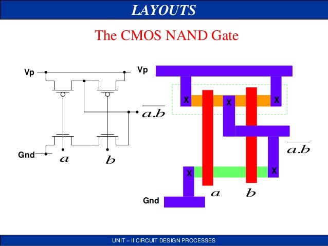
From what I can remember from my FPGA course, NAND all the things! Let's take the FPGA as the chip example, it stands for "field programmable gate array". It is basically like a sandbox of logic chips whose connections is determined by some program that is compiled. The chips at a very basic level are probably all NAND gates. If you're not familiar with logic theory if you pass inputs through a particular gate, you get some output. These gates have different behaviors. An AND gate for example outputs true if all inputs are true, false otherwise. Similarly an OR gate outputs true if any of its inputs are true, false otherwise. NAND gates produce the opposite output of an AND gate. NANDs are also very special in that they can be combined with other NANDs to produce any other logic gate. A NOT gate for example negates the input (input=true, output=false). A NOT gate behavior can be created by taking the single input and passing it as both inputs to a NAND gate (in1=true, in2=true, in1 AND in2 = true, therefore in1 NAND in2 = false, try this with in1/in2=false). Going even deeper, a NAND logic can be created from electronic components called transistors. Basically think of a transistor as a water valve: water from a source comes into the valve, there's an output, and the valve itself which controls the flow. Same concept in electronics, you have a voltage source on one end, a voltage output on the other, and a voltage input, where if triggered, allows flow from the source to the output. I forget the exact circuit but a NAND gate is created by some combination of these transistors. And that's how you get the circuitry inside these chips.
Of course, this information is probably dated and chip design has most likely changed over the years but this is how I've always understood it.
Of course, this information is probably dated and chip design has most likely changed over the years but this is how I've always understood it.