If you think 2 % change in MAX clock when it sees taxing code for an instant is same proportionately as 560 max to 336 max then thats your call.
I have been spending some time trying to understand the memory architecture of the XSX and its comparison to the PS5. I thought I understood it last week but now there are quite a few things that are quite mysterious to me.
Let me go over what I do understand and work my way from there. Anyone with a better understanding please jump in and clarify where necessary.
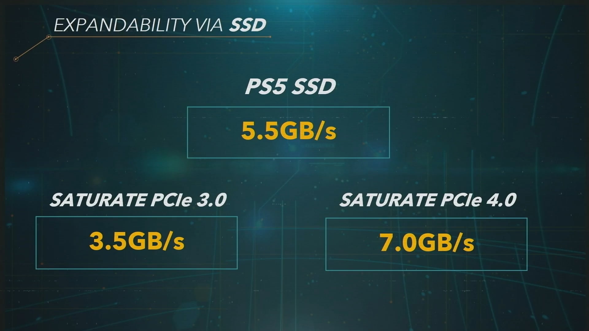
Each VRAM1 lane on both the XSX or PS5 is 56GB/s.
The PS5 has 8 lanes for a total of 8*56 = 448 GB/s of shared bandwidth. Each lane has two 16 bit channels = 8 * (2*16)= 256 bit bus.
Xsx has 10 lanes with 56 GB/s each for 560 GB/s total. Each of those lanes also have 2 16 bit channels. 10*32=320 bit bus.
Each consumer of RAM on each device can consume a whole channel's bandwidth (aka 56GB/s)
So if the PS5 CPU accesses 4 lanes of memory, the CPU will consume 224GBs and 8/16 GB for the GPU. In the PS5 each channel is ostensibly connected to a 2GB ram chips which both CPU and GPU can fully consume or not.
In XSX, the memory is logically split into 6lanes with 2GB chips and 4 lanes with 1 GB chips..
The GPU can see the 4 lanes with the 1 GB chips all the time as well as the lower 1 GB chips in the 6 lanes with 2GB. = 10 GB.
The CPU has been given priority over the top 1GB of the 6 lanes with 2GB chips =6B.
If the CPU chooses to consume all 6 lanes * 56Gb/s = 336 GB and 6GB of slow ram and maybe 6GB of fast ram? This is unknown.
Or would the CPU and GPU share the lane bandwidth and each use 28Gbs and interleave their access? So that the CPU is accessing 6*28GB/s for 168GB/s while the GPU is running at 168+224=392GB per Second to get 10GB.
If not, The GPU is left with 224GB to consume over the four remaining 1GB lanes. (= to what would happen in a split PS5 scenario.) But only 4 GB!
The total bandwidth is still 336+224 =560GB/s.
Conversely if the GPU consumed all lanes it would get 10GB of VRAM storage at 560GB/s. But what happens to the top 1GB of each of the 2GB lanes? Are they dormant and unused?
If the CPU consumed 1/6 would it consume the full 2 Gb of RAM, and the GPU would get 9GB of VRAM at 9*56=504GB/s and the CPU 56GB/s and so on. Or would it consume only the top 1GB while blocking the GPU from accessing the bottom 1GB chip?
Consumption is always equal to total buswidth and speed available.
Now do I like that design? Not really. Because I don't understand as of yet what happens with the "leftover" RAM of one or the other device consumes a full VRAM lane.
Hope I didn't confuse things even more.
 I think retailers here in the UK are just trying to ship as many as possible. You can get the One X for £250 which is a bargain considering the PS4 Pro is holding it's value at £350
/cdn.vox-cdn.com/uploads/chorus_asset/file/19811686/storage.jpg)