
http://www.chipworks.com/en/technical-competitive-analysis/resources/blog/inside-the-xbox-one/
Compared to the PS4 (left), you can see the where the resources were dedicated;
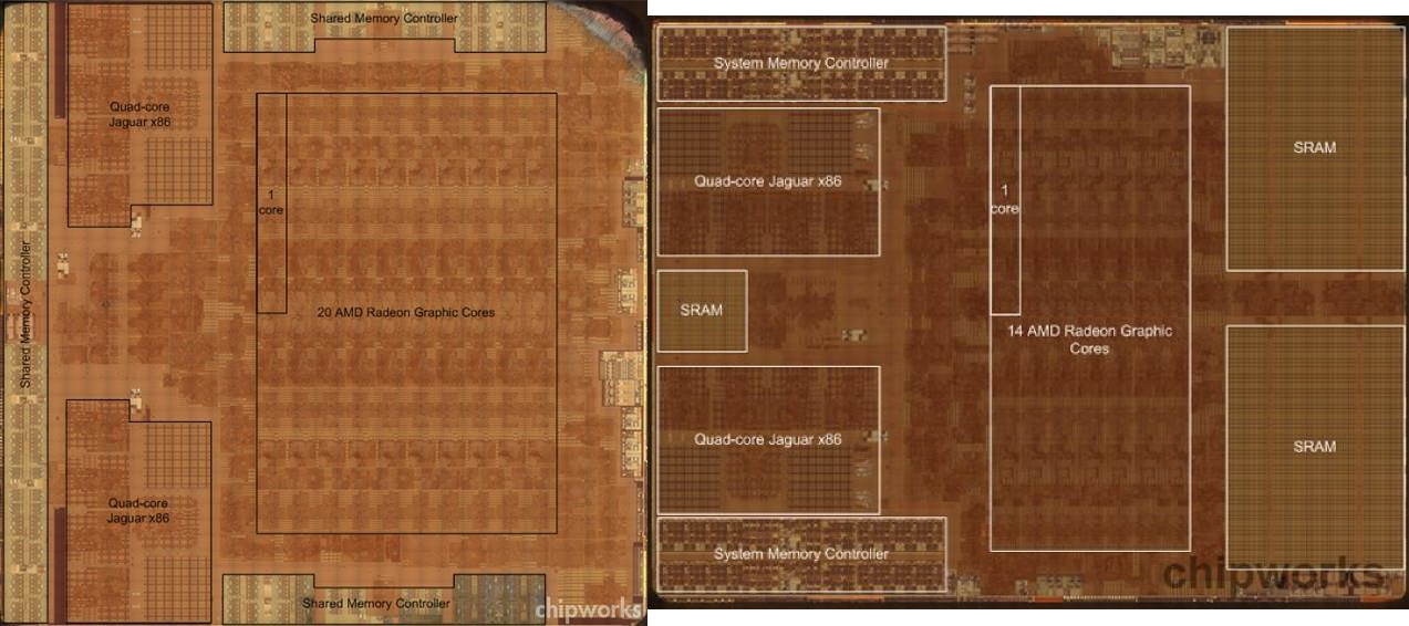
Expected but still insane how much real estate ESRAM takes up.
Expected but still insane how much real estate ESRAM takes up.

Max 4CU more.Can I take a system with the die size of the Xbox but dedicated to GPU - looks like you could squeeze 28CUs on there, then the GDDR5 of the PS4?
It's the CPU cache, no?It's interesting that the SRAM is divided 3 ways like that, that doesn't make sense.
The small block SRAM is for the secret sauce dGPU?LOL
It was confirmed to be present in the external power brick.Has anyone spotted the dGPU yet?
It's the CPU cache, no?
No, CPU caches are inside the Jaguar outlines. That is something else, looks to be 2-3MB extra SRAM there for something. Maybe SHAPE but that's an excessive amount of SRAM for an audio chip.It's the CPU cache, no?
No, CPU caches are inside the Jaguar outlines. That is something else, looks to be 2-3MB extra SRAM there for something. Maybe SHAPE but that's an excessive amount of SRAM for an audio chip.
It's the CPU cache, no?
Wait, didn't the PS4 have 18 graphic cores? The picture says 20.
Maybe I'm misremembering, but I'm pretty sure it was rumored to have 18 cores.
I'd guess that's the SHAPE + Kinect processing block, along with its own embedded SRAM.The Wii U GPU also has some random extra blobs of embedded memory thrown in there. Maybe they both just use it as a quick access scratchpad.
2 disabled for redundancy.Wait, didn't the PS4 have 18 graphic cores? The picture says 20.
Maybe I'm misremembering, but I'm pretty sure it was rumored to have 18 cores.
misterX's herd is in full on meltdown mode trying to figure out how to explain these pictures...
that's exactly the logic the misterxmedia morons are using. funny they haven't caught on to being lied to for the last 2 years by their "insiders"
Is the xbone's die size bigger than the ps4's die size?
Wait, didn't the PS4 have 18 graphic cores? The picture says 20.
Maybe I'm misremembering, but I'm pretty sure it was rumored to have 18 cores.
I was wondering why no one had made this thread yet, also I haven't seen a thread about the Kinect tear down.
Edit:
Extra SRAM between the CPU is new
~5% bigger.Is the xbone's die size bigger than the ps4's die size?
Wait, didn't the PS4 have 18 graphic cores? The picture says 20.
Maybe I'm misremembering, but I'm pretty sure it was rumored to have 18 cores.
18 compute units functioning, 2 disabled to improve yields (if two go bad, they can disable those ones instead of toss the chip)
The two huge ESRAM squares are 16MB each. There is no way that little island is 15MB, it's 2-3 MB tops.it's not, they said at the hotchips event I believe that there was an additional 15mb of esram for the cpu.
Wait, didn't the PS4 have 18 graphic cores? The picture says 20.
Maybe I'm misremembering, but I'm pretty sure it was rumored to have 18 cores.
They don't have "insiders". It's just the same guy talking to himself.
it's not, they said at the hotchips event I believe that there was an additional 15mb of esram for the cpu.
I've been eagerly awaiting that comment section in his latest post to update to show what kind of asinine discussion they come with for this.
no, what they said was there there was a total of 47MB of onboard storage...they didn't say anything about what it was or what kind...it's not, they said at the hotchips event I believe that there was an additional 15mb of esram for the cpu.
Dat huge SRAM. Was this purely a measure to compensate for the DDR3? Why didn't they just go the GDDR5 route?
Dat huge SRAM. Was this purely a measure to compensate for the DDR3? Why didn't they just go the GDDR5 route?
it's not, they said at the hotchips event I believe that there was an additional 15mb of esram for the cpu.
