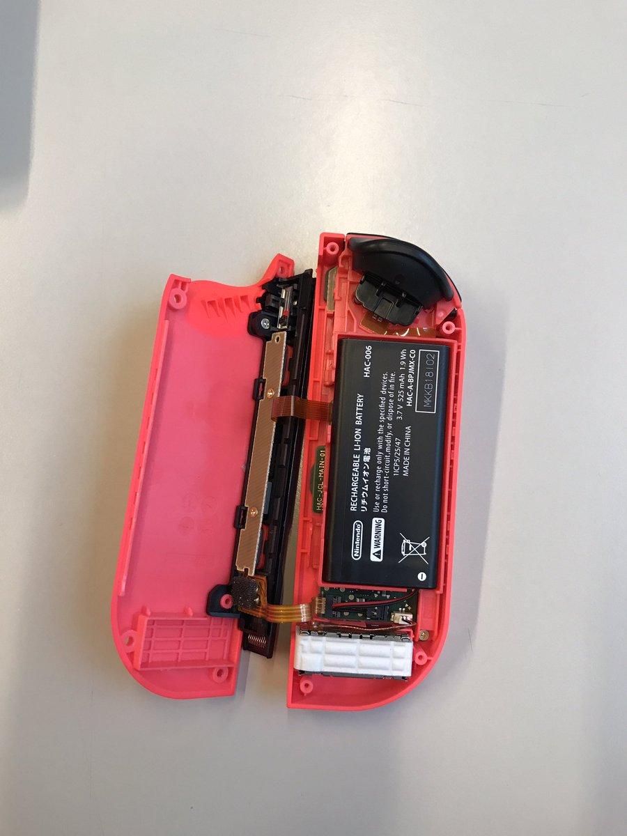
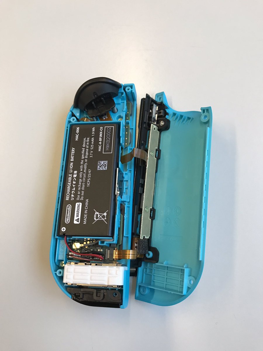
Someone finally opened up a Joycon for those interested:
https://twitter.com/linkees/status/836579448518557698
The batteries seems to be once again very easy to replace which is a good thing.
I guess a teardown of the retail switch will follow soon.
Someone finally opened up a Joycon for those interested:
https://twitter.com/linkees/status/836579448518557698
Far less than the TX1, or any other (full clocked, the Switch clocks were obviously chosen to never throttle) high performance mobile ARM chip out there.
That's the 6S, can't find the 7 but it got even better on throttling.
Yeah results seem really solid for a device of that size, but still not good enough for a proper console. Anyway, i doubt the iPhone outperforms the Switch GPU wise, the CPU is obviously much better..
Someone finally opened up a Joycon for those interested:
https://twitter.com/linkees/status/836579448518557698
Yeah results seem really solid for a device of that size, but still not good enough for a proper console. Anyway, i doubt the iPhone outperforms the Switch GPU wise, the CPU is obviously much better.
So the short of it would be the A10 rolls even the Shield TVs CPU at full clocks, the Switch has little chance there. The Shield TV enjoys enough thermal overhead to still be beating the iPhone 7 on the GPU side, but at docked clocks the Switch would be close-ish, while undocked obviously it's around half of its full performance.
It's crazy that Apple just decided to get serious about building ARM cores and started consistently rolling everyone year over year, I guess that happens when you buy PA Semi and Intrinsity and actually keep the talent and manage it well. I think an Apple TV that kept up to date with iPhone chips and maybe with a heatsink and active cooling would be one beast of a microconsole, with more storage.
If Apple thought they could be wildly profitable making game consoles, they certainly could, but I think the margins are too low for them.
In terms of performance, I think you're seriously underselling how much of a difference there is between making games for iOS/Android on general purpose devices vs. a custom kit dedicated to gaming with lots of Nvidia, Nintendo, and middleware support.
can anyone tell me how it compares to other mobile SoC like Apple's A10 or Snapdragon 821?
Don't know if this has been mentioned yet but Nintendo's Japanese support site says the Switch supports UHS-I Class 1 cards (just like those licensed HORI cards).
"Q: What microSD cards could be used with the Switch?
A: Nintendo Switch can support microSD/microSDHC/microSDXC memory cards.
It also supports the UHS-I standard as well as UHS Speed Class 1."
--------------
On other news, the SD Association has just introduced the UHS-III standard which still utilizes the same layout as UHS-II cards.

You need to clarify what you mean by v10 and v30. UHS-I is SD v3.01, UHS-II is SD v4.0 and UHS-III is SD v6.0.So UHS-1 V10 would be the max supported, and not UHS-1 V30?
You need to clarify what you mean by v10 and v30. UHS-I is SD v3.01, UHS-II is SD v4.0 and UHS-III is SD v6.0.
https://en.wikipedia.org/wiki/Secure_Digital#Ultra_High_Speed_.28UHS.29_bus
You need to clarify what you mean by v10 and v30. UHS-I is SD v3.01, UHS-II is SD v4.0 and UHS-III is SD v6.0.
https://en.wikipedia.org/wiki/Secure_Digital#Ultra_High_Speed_.28UHS.29_bus
I'd guess they're probably actually talking about the U1 and U3 speed classes.

The SD consortium is an example of how _not_ to make speed rating systems for the consumer. That's why most vendors adhere to providing the UHS class (I, II, III) which tells the bus capability of the card, and the top read speed (e.g. 45MB/s).Ah yeah, sorry, I was referring to this picture:
So U1/U3, which apparently is the same speed as V10/V30.
It's weird since some cards have different symbols yet the same speed (like the circled 10 being apparently the same as U1).

Can someone here explain to me why the gaming media (such as Gamespot etc.) seem to report on roughly 1 TF for the Switch when much lower numbers are being used in here?
I am trying to calm some people down who expect Xbone-like power levels but all the sources I can find online are pointing at those 1 TF...
There was a report from some website that said it was 1 TFLOPS, but that was in half-precision numbers, whereas it is normal to give the FLOPS in full precision numbers, which is 512 GFLOPS. Beyond that, the report didn't take into account that this system has a lower clock speed than the stock Tegra X1, which decreases the FLOPS count to 393 GFLOPS when docked and 197 GFLOPS when undocked. The report that all those news sites are running was plain wrong, and showing an annoying lack of basic understanding of what they were reporting.Okay I am not a techie but I've been trying to follow this post.
Can someone here explain to me why the gaming media (such as Gamespot etc.) seem to report on roughly 1 TF for the Switch when much lower numbers are being used in here?
I am trying to calm some people down who expect Xbone-like power levels but all the sources I can find online are pointing at those 1 TF...
Is that reddish brown stuff the thermal paste? What the fuck.
Thanks for posting this, it's nice to have a higher resolution image. Comparing it to the images in the OP, it seems the prior photos were of a unit with a non-final battery, but everything else seems to be the same (from what I can see).
The bottom right portion of the unit in this image
looks substantially different than in the above one. Although this other image from the OP:
looks the same. It seems like a component was removed from that area in the first image, any ideas what it was?
There's a metal panel between the Switch's innards that you see there and the rear of the case. The thermal paste is there to provide a thermal connection to this panel to allow the system to passively dissipate heat more effectively when the fan is off.
Game card slot, no?
Someone finally opened up a Joycon for those interested:
https://twitter.com/linkees/status/836579448518557698
Most likely its just fp16 numbers for X1(while fp32 is 500GFLOPs) nvidia specs and at full clock speeds. According to eurogamer leaked specs from dec(and they seem pretty sure about it even now) the final dev clockspeeds were downclocked. GPU by like 25% and CPU clockspeeds are cut in half, due to conserving battery life and throttling from heat.Okay I am not a techie but I've been trying to follow this post.
Can someone here explain to me why the gaming media (such as Gamespot etc.) seem to report on roughly 1 TF for the Switch when much lower numbers are being used in here?
I am trying to calm some people down who expect Xbone-like power levels but all the sources I can find online are pointing at those 1 TF...
The bottom right portion of the unit in this image
looks substantially different than in the above one. Although this other image from the OP:
looks the same. It seems like a component was removed from that area in the first image, any ideas what it was?
Edit:
So here's something interesting: the left and right joy-cons have different antenna configurations:
Following recent reports of the left joy-con not having quite as good wireless connectivity as the right one, it's interesting to see that they do have physically different antenna configurations. On the image of the right joy-con we can see the antenna connection on the PCB, and a wire running to a metal plate, which it's soldered to. This metal plate is likely acting as the antenna (and may wrap around out of view of this photo).
On the left joy-con, though, we don't see the antenna connector, the wire or the metal plate. The joy-con definitely has an antenna (it physically has to to transmit wireless signals), but it's not visible in this photo, and it's different to the antenna Nintendo is using in the right joy-con. That's not necessarily to say that it's worse, but it's not the same.
It's interesting to consider why Nintendo didn't just use the same antenna configuration between both units. It's possible that the extra data transferred by the right joy-con while using the infra-red camera on the bottom required a higher quality connection with Switch, so they upgraded it to a beefier antenna while leaving the left joy-con one as-is.
As Graphics Horse says, there's a daughter board for the game card slot (and headphone jack) which was removed in the first photo (presumably to get photos of it, as they posted a separate photo of the daughter board on its own).
Here's something interesting I noticed on the new photo, though. There's a small low-profile connector on the motherboard which isn't connected to anything:
This is also unconnected in all the other photos we've seen, and none of the components we've seen would interface with it. It's also in a position where there really wouldn't be much space for anything to sit if it were connected.
One theory that did occur to me is that it's an alternative for the eMMC connector. That is, it's designed for a small board which sits above the wifi/bluetooth module, just as the eMMC board does, but which needs a different interface. This could be embedded UFS (or even in theory BGA NVMe), and it would help explain why the eMMC module is on its own board in the first place.
Edit:
So here's something interesting: the left and right joy-cons have different antenna configurations:
Following recent reports of the left joy-con not having quite as good wireless connectivity as the right one, it's interesting to see that they do have physically different antenna configurations. On the image of the right joy-con we can see the antenna connection on the PCB, and a wire running to a metal plate, which it's soldered to. This metal plate is likely acting as the antenna (and may wrap around out of view of this photo).
On the left joy-con, though, we don't see the antenna connector, the wire or the metal plate. The joy-con definitely has an antenna (it physically has to to transmit wireless signals), but it's not visible in this photo, and it's different to the antenna Nintendo is using in the right joy-con. That's not necessarily to say that it's worse, but it's not the same.
It's interesting to consider why Nintendo didn't just use the same antenna configuration between both units. It's possible that the extra data transferred by the right joy-con while using the infra-red camera on the bottom required a higher quality connection with Switch, so they upgraded it to a beefier antenna while leaving the left joy-con one as-is.
http://www.eurogamer.net/articles/digitalfoundry-2017-nintendo-switch-reviewFor perspective, while docked the Switch demands 7.5 watts on the main menu, and 16 watts at peak during games.
Digital Foundry
http://www.eurogamer.net/articles/digitalfoundry-2017-nintendo-switch-review
How does these power draw numbers line up with expectations/speculation about the Switch's hardware?
I've never seen anyone in these threads suggest wattage that high, even for docked mode on Maxwell architecture. With Eurogamer clocks, and their assumption that very little changes were made to the Tegra chip, shouldn't we be seeing much lower numbers? Does this hint at potentially higher clocks on retail devices, some other changes/additions to the SoC, or heck, maybe even some poor design choices here and there in the system? What say you guys?
As Graphics Horse says, there's a daughter board for the game card slot (and headphone jack) which was removed in the first photo (presumably to get photos of it, as they posted a separate photo of the daughter board on its own).
Here's something interesting I noticed on the new photo, though. There's a small low-profile connector on the motherboard which isn't connected to anything:
This is also unconnected in all the other photos we've seen, and none of the components we've seen would interface with it. It's also in a position where there really wouldn't be much space for anything to sit if it were connected.
One theory that did occur to me is that it's an alternative for the eMMC connector. That is, it's designed for a small board which sits above the wifi/bluetooth module, just as the eMMC board does, but which needs a different interface. This could be embedded UFS (or even in theory BGA NVMe), and it would help explain why the eMMC module is on its own board in the first place.
Edit:
So here's something interesting: the left and right joy-cons have different antenna configurations:
Following recent reports of the left joy-con not having quite as good wireless connectivity as the right one, it's interesting to see that they do have physically different antenna configurations. On the image of the right joy-con we can see the antenna connection on the PCB, and a wire running to a metal plate, which it's soldered to. This metal plate is likely acting as the antenna (and may wrap around out of view of this photo).
On the left joy-con, though, we don't see the antenna connector, the wire or the metal plate. The joy-con definitely has an antenna (it physically has to to transmit wireless signals), but it's not visible in this photo, and it's different to the antenna Nintendo is using in the right joy-con. That's not necessarily to say that it's worse, but it's not the same.
It's interesting to consider why Nintendo didn't just use the same antenna configuration between both units. It's possible that the extra data transferred by the right joy-con while using the infra-red camera on the bottom required a higher quality connection with Switch, so they upgraded it to a beefier antenna while leaving the left joy-con one as-is.
Confirmation the joycon issue is hardware related and can't be fixed with a fw update then.
Well, the Left and Right Joy-Cons are different. You can read amiibo on the right Cons but not the Left Cons. But I'm not sure how that'd change anything. The right also has that IR pointer on the bottom on it.
Confirmation the joycon issue is hardware related and can't be fixed with a fw update then.
-snip-
We are close to real answers, at least we aren't getting shell shocked from our speculation as Eurogamer's clocks were definitely real and gave us the minimum spec that has already been improved on with the performance boost Eurogamer detailed. I'm glad we will be able to stop speculating on hardware soon, this is by far my favorite hardware design from Nintendo and they did a great job with performance. Battery life does seem to be a possible problem, so it will be confusing if Switch is indeed 20nm because they could have avoided this problem with a shift to 16nm. I get my switch in about 40 hours (when I'll actually pick it up) I won't be opening it up, but I'll help dig into whatever information comes in here, as long as I'm not busy playing Zelda that is.
Indeed... my theory is that the left joycon actually communicates with the right through a different protocol, not Bluetooth. I guess we could test that by removing the right joycon from range and see if the left still connects... the left needs much less bandwidth since it's just standard inputs. Also the configurations of joycon supported would exceed the max 7 (plus host) the Bluetooth has.Following recent reports of the left joy-con not having quite as good wireless connectivity as the right one, it's interesting to see that they do have physically different antenna configurations. On the image of the right joy-con we can see the antenna connection on the PCB, and a wire running to a metal plate, which it's soldered to. This metal plate is likely acting as the antenna (and may wrap around out of view of this photo).
On the left joy-con, though, we don't see the antenna connector, the wire or the metal plate. The joy-con definitely has an antenna (it physically has to to transmit wireless signals), but it's not visible in this photo, and it's different to the antenna Nintendo is using in the right joy-con. That's not necessarily to say that it's worse, but it's not the same.
It's interesting to consider why Nintendo didn't just use the same antenna configuration between both units. It's possible that the extra data transferred by the right joy-con while using the infra-red camera on the bottom required a higher quality connection with Switch, so they upgraded it to a beefier antenna while leaving the left joy-con one as-is.
There was a report from some website that said it was 1 TFLOPS, but that was in half-precision numbers, whereas it is normal to give the FLOPS in full precision numbers, which is 512 GFLOPS. Beyond that, the report didn't take into account that this system has a lower clock speed than the stock Tegra X1, which decreases the FLOPS count to 393 GFLOPS when docked and 197 GFLOPS when undocked. The report that all those news sites are running was plain wrong, and showing an annoying lack of basic understanding of what they were reporting.
Edit:whelp someone already said half precision(meaning fp16).
Such a strange choice to have one with and one, seemingly, without an extra antenna. Possibly that these two are still two different batches for some reason (as in a newer left joy-con potentially also having an antenna)? Anyone else happened to have opened the joy-con?
Indeed... my theory is that the left joycon actually communicates with the right through a different protocol, not Bluetooth. I guess we could test that by removing the right joycon from range and see if the left still connects... the left needs much less bandwidth since it's just standard inputs. Also the configurations of joycon supported would exceed the max 7 (plus host) the Bluetooth has.
Well well. Is the Switch the second console this generation to run FreeBSD?
Lol I actually decided not to answer that idiot after I saw someone already started discussing with him!Thanks a lot guys! I'll admit that I started a commenting war with a user on Amazon.de that just loves to spread false information, such as the power of the Switch being almost on par with Xbox One. Sadly a lot of the German gaming media seems to have referenced that VentureBeat/Gamespot report from December, reporting it basically as facts.
Great, this should end the clocks talk pretty quickly. Chipworks will do the rest with the node.Marcan has already one and it seems that the OS is based on FreeBSD.
https://twitter.com/marcan42/status/837481011508195329
Great, this should end the clocks talk pretty quickly. Chipworks will do the rest with the node.
Great, this should end the clocks talk pretty quickly. Chipworks will do the rest with the node.
So how long do we expect before someone breaks it down with scans? How long does it usually take a site like chipworks?
Dont really have to do that, as I hid my right away and left behind my back 5 meters was operational.That's a really interesting theory, I hadn't thought of that. If you wanted to be absolutely sure you could detach the battery in the right joycon before testing (it looks easily detachable from the photo).