Yeah I figured it shouldn't be too CPU intensive, it's just something that does take a bit of the CPU away from the main game. And that's a very interesting thought about the revamped physics engine... I wonder how much input Nvidia had with the HD rumble. I would have thought Immersion's licensed software would have most of that work done. Maybe Nvidia just helped merge that with their own NVN API.
I would imagine that what Nvidia could contribute would be simple integration with the game's physics system (so what you feel is calculated based on the physical properties of the objects in game, for example if your sword hits a particular object PhysX could use the speed of the collision and the material properties of both objects to calculate the appropriate signal to be sent to the linear actuators).
I guess I would just say that it seems unlikely given what we know, but I guess possible, that the 1.78GHz CPU speed is solely for emulation. It still likely wouldn't explain how you can get 4 A57s to 1.78GHz and a 20nm 2SM Maxwell GPU to 921MHz continuously for 8 days when a Shield TV can't do that without throttling and has a much larger volume, and thus much better heat dissipation.
Add to that the fact that no one from any of the Switch events have felt air coming out of the vents even when docked playing Zelda, and it looks quite possible that they have built this on a 16nm node.
We don't strictly know how many CPU cores were being used during the tests. If they were using Nvidia's Vulkan fish demo, then that's not something designed to stress CPUs, and depending on how the test was configured, it's possible that they were only using a single core.
Even if it's docked-only, I find it pretty unlikely that they'd make clocks available for VC but not native games. The only thing where they've really done something like that before is relaxing the NX bit enforcement so VC stuff could use JIT compilers, and that is was likely more for security than anything else.
It's strange, but this is also a very different device than anything Nintendo's developed before, and balancing portable and docked modes may force them to make very different decisions on things like this than they would have made previously. For example, I have no doubt that they could clock the CPU higher in docked mode than portable without much issue, but they seem to have made the decision to limit them to the same CPU clock to simplify development across the two performance targets.
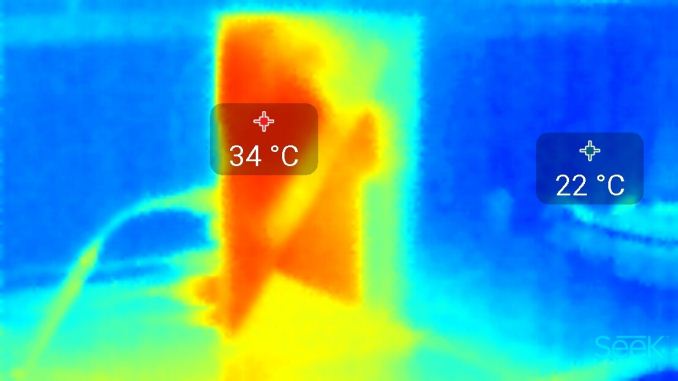
So someone on Reddit managed to bring a heat vision camera in while trying out the Switch and got a bunch of photos of the device playing different games:
www.imgur.com/gallery/egT5E
Note at least at one point the person believes the fan was indeed running actively in portable mode.
That's pretty interesting, particularly that you can see the heat being transferred through the joycon rail on the right hand side of the system (which shouldn't be that surprising in retrospect, as it's metal, so will conduct heat much better than the plastic & glass used for the rest of the casing).
Depends on what CPU and what process is being used. If we assume 3 hours is the battery life at the original 1ghz CPU speed and its 16nm A72 then upping to 1.7Ghz should drop that by about half an hour or even less.
Yeah, it should be about half an hour based on my calculations. It would seem strange to not just allow those clocks in the first place, though, if they were fine with that battery life. If they're concerned with, for example, getting western third-party ports, then increasing the CPU clocks a year or two down the line isn't going to do them much good on that front.
If we assume four CPU cores with one for the OS and three for games. Then 3x A57 at 1Ghz would be about half the performance of 6x Jaguar at 1.6Ghz (PS4 CPU). While 3x A72 at 1.7Ghz would be about the same as 6x Jaguar at 1.6Ghz.
There is the possibility that the Switch CPU has extra cores just for the OS (A53 most likely). That would change things a bit, obviously giving a extra 33% CPU performance for games (4 cores instead of 3 for games).
As far as WiiU goes, that's much harder to say for certain as we have no direct comparison. Though its safe to say A57 at 1Ghz would certainly be faster core for core.
I'd be quite surprised if there weren't a couple of A53 or A35 cores being used for the OS. They're small, they sip power, and they're surprisingly capable, particularly when it comes to crypto. Devoting an A57 or A72 to the OS would seem like a waste of die space and power draw in comparison. They would need to move to a HMP model (compared to TX1's clustered switching), but Nvidia have shipped Parker with (presumably) their own HMP interconnect, or Nintendo could have just used one of ARM's CCI interconnects to do the job.
Thanks for posting this. I'm going to do a separate post digging into the details in a bit (this post is long enough as it is).
Doesn't this:
basically mean there is no way to connect the normal Switch to a base with this SoC due to the lack of bandwidth in USB 3.0?
EDIT: Ah, or this future "SCD" dock might have a different type of connector? I guess that could work then.
They don't need a different connector. USB-C is a physical interface that was specifically designed to be able to handle arbitrary communication protocols via the alternate mode specification. Obviously we have things like DisplayPort alt mode (which Switch uses while docked) and Thunderbolt, but manufacturers can also design their own proprietary alt modes in pretty much whatever manner they want, without having to publish them or be certified by USB-IF or anything like that.
There are basically two options for communicating with a dock containing a GPU or some other computational hardware. The first is to simply use the USB protocol, and despite the leakers claims, there's no reason to believe they would be limited to USB 3.0 speeds. We know that the system uses DisplayPort alt mode, which operates by interleaving a 5Gb/s USB signal with a 5Gb/s DisplayPort signal. This means that the system is limited to 5Gb/s
while also outputting video, but it also means that it's capable of signalling at 10Gb/s, meaning full USB 3.1 speeds are entirely possible if the system isn't outputting a video signal as well (which it wouldn't be for a performance enhancing dock).
The other option is that they define their own alt mode. USB, Thunderbolt, DisplayPort, etc., are all protocols intended for use over cables, perhaps over a distance of 5 metres or more, and require far tighter tolerances on signalling at a given frequency to accommodate signal degradation and interference over those lengths. Short-range protocols (where wire length is measured in centimetres, rather than metres) can hit far higher speeds at much lower cost, and if they wanted to they could co-opt one of these over the USB-C connection as an alt mode. As a simple example, then could run 2 PCIe 3 lanes giving 2GB/s of bandwidth both ways, or an asymmetric M-PHY (4 lanes up, 1 lane down) giving up to 2.3GB/s of data from Switch to dock. If they really wanted to push it, they could even get 5GB/s out of a dual-lane NVLink 1 connection, and as ridiculous as that sounds, it would almost certainly be a lot cheaper and simpler to implement than Thunderbolt. Given that it's purely an interface for use between their own products, they could even adopt a variation of any of these, increasing clock speed or moving to an asymmetric or half-duplex transmission system (which would increase usable bandwidth at a given clock speed over a symmetric full-duplex protocol, given Nintendo's use case is likely to be far from symmetric).
I think we're also overestimating the amount of bandwidth required for a something like this. The GTX 980 achieves
about 75% of its max performance at 1080p while on a PCIe v1 x4 link, which is only
1GB/s of bandwidth. Some games are an even lower performance differential than this, but in all cases we're talking about Windows games running on DX11. A game built in Vulkan for Switch and decently optimised around the bandwidth available could likely get by on quite a bit less.
")