• Hey, guest user. Hope you're enjoying NeoGAF! Have you considered registering for an account? Come join us and add your take to the daily discourse.

The Curious Case of the Switch Foxconn Leak (Now a hardware fanfiction thread)

KingSnake

The Birthday Skeleton
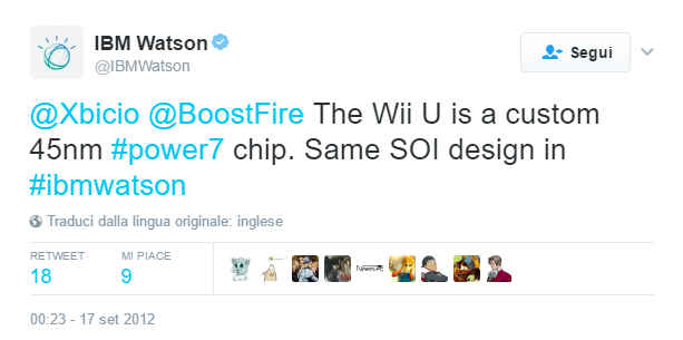
It's still an official social media account of a company that's pretty much related with the whole thing. Until they pull it out I don't see any reason to doubt it.

Anonymous Foxconn leaks are real news but real social media accounts are fake. Interesting world we live in.
 

Rodin

Member
It's still an official social media account of a company that's pretty much related with the whole thing. Until they pull it out I don't see any reason to doubt it.

Anonymous Foxconn leaks are real news but real social media accounts are fake. Interesting world we live in.

2hqxi07wuujw.jpg


immaginel0qzw.png
 

Rodin

Member
How long before those were deleted? So I know how long I need to watch the ARM page?

The second one is still up, they corrected themselves in another one though. Not sure about the first one, found it on the internet.

The ARM post will likely be deleted, but it will just mean that Nintendo got pissed at them lol.

EDIT: btw, i'm not saying that it certainly doesn't use A57. Just that this particular post isn't necessarily as reliable as you're suggesting.

EDIT2: aaaand gone lol
 

z0m3le

Banned
So thinking about the cooling solution and the fan reportedly active while portable. The Foxconn leak states that the switch is indeed 16nm, if both of these reports are true, Eurogamer's clock doesn't make sense, 1ghz A57 would draw less than a watt on 16nm (55% power reduction) the gpu would also be very light at 16nm,the entire SoC would use about a watt, which with the cooling described in the leak would never let the chip get warm enough to need a fan.

I was 60/40 on these clocks before, but I find the eurogamer clocks must have been changed, because this device would need to draw around 4 to 5 watts to give us anything like those thermal pictures.

We can just look at the X1 and tell that this device should be much cooler at 16nm with half the cpu and gpu clocks.
 

Noitshado

Member
Would it be possible for them to do like a boost mode like the PS4 Pro? Like say the DF spec is the target spec for developers but retail units will run at 20-30% higher clockspeeds to act as a buffer for performance spikes. Im running on the assumption Nintendo develops with 20-30% less than maximum potential of hardware with good optimizations and clever art design to keep such solid performance in their games. So if they mandate all devs target a lower than retail spec, games system wide would have solid performance. If they design it like that right out of the gate and provide good documentation and tools to avoid weird programming and design conflicts, would it be viable either at launch or later through updates?
 

z0m3le

Banned
Would it be possible for them to do like a boost mode like the PS4 Pro? Like say the DF spec is the target spec for developers but retail units will run at 20-30% higher clockspeeds to act as a buffer for performance spikes. Im running on the assumption Nintendo develops with 20-30% less than maximum potential of hardware with good optimizations and clever art design to keep such solid performance in their games. So if they mandate all devs target a lower than retail spec, games system wide would have solid performance. If they design it like that right out of the gate and provide good documentation and tools to avoid weird programming and design conflicts, would it be viable either at launch or later through updates?

Wouldn't make sense given battery life imo, also nothing about the Foxconn leaks suggest this, the SCD could however be used in this way, but I expect developers to be able to use whatever is there.
 

Noitshado

Member
Wouldn't make sense given battery life imo, also nothing about the Foxconn leaks suggest this, the SCD could however be used in this way, but I expect developers to be able to use whatever is there.

Hmm I see. Battery life is definitely a problem. But possible that the given battery life estimates were in regards to the boosted clocks? Unless the wattage vs battery capacity lines up with 1Ghz. Foxconn rumor states 1.78ghz so between that and DF clocks I was thinking it was suggestive and could explain the difference in speeds. I also think it be a software related setting so the leaker wouldn't be able to know? The SCD if it exists I would think they'd make as a more substantial upgrade than just a buffer. But yeah seems unlikely Nintendo would limit devs in such a manner. Still, feels possible they would at least add a boost mode to a Switch Pro somewhere down the line and would put in the foundation starting out. Thx for scratching my brain itch lol.
 

Donnie

Member
So thinking about the cooling solution and the fan reportedly active while portable. The Foxconn leak states that the switch is indeed 16nm, if both of these reports are true, Eurogamer's clock doesn't make sense, 1ghz A57 would draw less than a watt on 16nm (55% power reduction) the gpu would also be very light at 16nm,the entire SoC would use about a watt, which with the cooling described in the leak would never let the chip get warm enough to need a fan.

Power consumption tells the same story. The device uses somewhere between 5w and 6w under full load (based on the lowest battery life estimate quoted by Nintendo). Like you say at 16nm and the frequencies described by Eurogamer we'd be looking at about 1w for the SoC. Really it should be using no more than 2-3w for the entire device. I don't even see where 5-6w would be going at 20nm with those Eurogamer clocks.
 
So thinking about the cooling solution and the fan reportedly active while portable. The Foxconn leak states that the switch is indeed 16nm, if both of these reports are true, Eurogamer's clock doesn't make sense, 1ghz A57 would draw less than a watt on 16nm (55% power reduction) the gpu would also be very light at 16nm,the entire SoC would use about a watt, which with the cooling described in the leak would never let the chip get warm enough to need a fan.

I was 60/40 on these clocks before, but I find the eurogamer clocks must have been changed, because this device would need to draw around 4 to 5 watts to give us anything like those thermal pictures.

We can just look at the X1 and tell that this device should be much cooler at 16nm with half the cpu and gpu clocks.

Well, two things: first, the thermals and cooling could make sense if it was 20nm with the Eurogamer clocks, right?

And second, how would the leaker actually know for sure if it's 16nm? All he can seemingly tell for sure about the physical configuration of the SoC is the size and that it's from Taiwan... I really doubt that he could tell through testing that it is 16nm, especially if his readout isn't telling him what CPU cores are being used. So I'd still take a healthy grain of salt with these specs.
 

z0m3le

Banned
Well, two things: first, the thermals and cooling could make sense if it was 20nm with the Eurogamer clocks, right?

And second, how would the leaker actually know for sure if it's 16nm? All he can seemingly tell for sure about the physical configuration of the SoC is the size and that it's from Taiwan... I really doubt that he could tell through testing that it is 16nm, especially if his readout isn't telling him what CPU cores are being used. So I'd still take a healthy grain of salt with these specs.

Are those thermals consistent with a x1 at 20nm and the eurogamer clocks?

What we know is that the Shield TV with X1 @20watts on 20nm has a similar heat performance as the Switch @5-6watts. We know this isn't possible on 16nm with Eurogamer's clocks because the device would draw about half the power, the 20nm version of this chip should have a similar power consumption to what the 16nm foxconn clocks have. IF he is right about the 16nm part though, the eurogamer clocks are outdated. The big point of contention here though is that A57 cores @ 1.78ghz and 921mhz for the gpu would be far too hot in the switch, it would draw nearly the same power and produce the same heat as the shield tv thanks to the battery, in such a small form factor, I don't think those clocks are possible and the entire point of testing at those clocks really does come into question with A57. If they moved from A57, there is no reason for them to stay on 20nm I don't think, Maxwell at 16nm already exists, we call it pascal, so the basic design is already in existence.

I find the only thing about the Foxconn leak to not make sense is Eurogamer's clocks being the shipped clocks.
 

Goodlife

Member
So, if it's 20nm, then the Eurogamer's clocks are probably right
If it's 16mn, then the Foxconn leaks clocks are probably right

Is that about it?
 
What we know is that the Shield TV with X1 @20watts on 20nm has a similar heat performance as the Switch @5-6watts. We know this isn't possible on 16nm with Eurogamer's clocks because the device would draw about half the power, the 20nm version of this chip should have a similar power consumption to what the 16nm foxconn clocks have. IF he is right about the 16nm part though, the eurogamer clocks are outdated. The big point of contention here though is that A57 cores @ 1.78ghz and 921mhz for the gpu would be far too hot in the switch, it would draw nearly the same power and produce the same heat as the shield tv thanks to the battery, in such a small form factor, I don't think those clocks are possible and the entire point of testing at those clocks really does come into question with A57. If they moved from A57, there is no reason for them to stay on 20nm I don't think, Maxwell at 16nm already exists, we call it pascal, so the basic design is already in existence.

I find the only thing about the Foxconn leak to not make sense is Eurogamer's clocks being the shipped clocks.

My question is, based on this new translation, how does this leaker seem to know that it's 16nm? He talks about it in the post describing the stress test, but he doesn't really connect his claim of 16nm to the CPU clocks, which is what we previously assumed was his chain of logic there.

So, why does he claim it's 16nm? Is that something he could possibly have seen?

So, if it's 20nm, then the Eurogamer's clocks are probably right
If it's 16mn, then the Foxconn leaks clocks are probably right

Is that about it?

Not necessarily. Eurogamer's clocks are probably right for launch software regardless of process node, but if it's 16nm then there's a chance the clocks could be increased to the Foxconn clocks (or already have been).
 

z0m3le

Banned
So, if it's 20nm, then the Eurogamer's clocks are possible, but the stress test clocks make no sense.

If it's 16mn, then the Eurogamer clocks are wrong, and the Foxconn clocks are likely.

Is that about it?

Fixed.

My question is, based on this new translation, how does this leaker seem to know that it's 16nm? He talks about it in the post describing the stress test, but he doesn't really connect his claim of 16nm to the CPU clocks, which is what we previously assumed was his chain of logic there.

So, why does he claim it's 16nm? Is that something he could possibly have seen?

He might have asked, it could have been known, he seems 100% sure about it in the SCD, so maybe there is a reasonable way to know? If he works at foxconn, I'm sure he has seen 16nm chips a lot so not sure but it is possible that he would know.


Not necessarily. Eurogamer's clocks are probably right for launch software regardless of process node, but if it's 16nm then there's a chance the clocks could be increased to the Foxconn clocks (or already have been).

Eurogamer's clocks are not possible if it's 16nm based on the thermal pictures we've seen. The device would draw less than 3 watts and with active cooling, run below room temperature. 16nm completely invalidates Eurogamer's clocks being used at these events.
 

Goodlife

Member
Not necessarily. Eurogamer's clocks are probably right for launch software regardless of process node, but if it's 16nm then there's a chance the clocks could be increased to the Foxconn clocks (or already have been).

I thought the heat shots further up this thread disproved the lower clocks at 16nm theory, as that wouldn't generate that much heat?
 
I thought the heat shots further up this thread disproved the lower clocks at 16nm theory, as that wouldn't generate that much heat?

Eurogamer's clocks are not possible if it's 16nm based on the thermal pictures we've seen. The device would draw less than 3 watts and with active cooling, run below room temperature. 16nm completely invalidates Eurogamer's clocks being used at these events.

All of the test units are plugged in and being charged, so it's possible they're all running with docked clocks. Not that likely, but possible.

If they are running in portable clock mode, then either its 20nm or they're running at the Foxconn clocks, yes.
 

z0m3le

Banned
"Today I saw a cube module near the bottom of the controller, could be a gyroscope. I'll ask around when I get a chance."
This is possibly how he knew it was 16nm, he seems to be stating fact, so I'll give him the benefit of the doubt, it is especially apparent that he is sure when it comes to the SCD but it is obviously days apart between the posts so it makes sense that his stance would solidify.

Cheers.
But we can discount 20nm running at Foxconn's clocks though, can't we. Battery life / heat would be crap and not fit in with what we know?

Yep
 
"Today I saw a cube module near the bottom of the controller, could be a gyroscope. I'll ask around when I get a chance."
This is possibly how he knew it was 16nm, he seems to be stating fact, so I'll give him the benefit of the doubt, it is especially apparent that he is sure when it comes to the SCD but it is obviously days apart between the posts so it makes sense that his stance would solidify.

That's an interesting point... Yeah, he could have asked someone who would know that. But then again, why would anyone at Foxconn know that? The SoC is manufactured at TSMC, so what purpose would there be having anyone at Foxconn (who isn't a Nintendo hardware design employee) know the detailed configuration of the SoC?

Maybe for testing purposes?
 

z0m3le

Banned
That's an interesting point... Yeah, he could have asked someone who would know that. But then again, why would anyone at Foxconn know that? The SoC is manufactured at TSMC, so what purpose would having anyone at Foxconn (who isn't a Nintendo hardware design employee) know the detailed configuration of the SoC?

Maybe for testing purposes?

Probably detailed on a list of hardware components... I really don't find that unlikely since they are putting these devices together, they likely have something like this.
There is also possibly a blue print somewhere for the device at foxconn.

With all the testing going on there, it really is not hard to see people knowing what is in the device. Especially surface level stuff like process node used.
 

Theonik

Member
There is no reason anyone at Foxconn would need to know the process node and it's not like they can easily peek into the silicon without stealing a chip.
 

z0m3le

Banned
There is no reason anyone at Foxconn would need to know the process node and it's not like they can easily peek into the silicon without stealing a chip.

This is an interesting fact, but we need to know that it is a fact and not your assumption. That is the problem I have with your post, is this knowledge you have about the inner workings of foxconn or just what you believe to be true? because if it is something you know, then we can discard his statement, otherwise it's hard to ignore him, and I don't mean to chase fanfiction, but this entire thread is about how correct this foxconn leaker was, and so far for every fact, he has been 100% correct.
 

z0m3le

Banned
that irks me that the mods allowed that last part to be added to the thread title.This has nothing to do with fanfiction. REALLY SILLY!

We started talking about a dock that could be more powerful than the PS4 Pro, even though it's seemingly a real device based on this leak, it's sort of hard to get people to believe that until there is some official word, it will come eventually unless it is scrapped altogether. At that point we will have another Nintendo hardware thread I'm sure and this title won't matter.
 
Is there some sort of simple run down that explains what you're discussing?
The Reddit post says the thing is confirmed to be a Devkit, and the impression I get is it's something similar to the Devkit image we saw immediately before the October reveal?
 
Is there some sort of simple run down that explains what you're discussing?
The Reddit post says the thing is confirmed to be a Devkit, and the impression I get is it's something similar to the Devkit image we saw immediately before the October reveal?

The Foxconn leak is talking about two (three actually) separate devices I believe. One is the final Switch retail units they are building and testing, one is a normal Switch devkit which apparently has 4g, and one is a devkit for a device that includes all of the Switch's normal internals, but also another huge GPU on top of that.
 

sits

Member
We started talking about a dock that could be more powerful than the PS4 Pro, even though it's seemingly a real device based on this leak, it's sort of hard to get people to believe that until there is some official word, it will come eventually unless it is scrapped altogether. At that point we will have another Nintendo hardware thread I'm sure and this title won't matter.

Indeed. This is the new Switch HW speculation thread (RIP, the amazing MDave throttles his X1 thread), irrespective of what the current title literally says. Thus, please state speculation when it is indeed just that, as we're trying to compile empirical info.
 
The Foxconn leak is talking about two (three actually) separate devices I believe. One is the final Switch retail units they are building and testing, one is a normal Switch devkit which apparently has 4g, and one is a devkit for a device that includes all of the Switch's normal internals, but also another huge GPU on top of that.
But did it get further than the guy assuming it was a GPU?
We've seen two types of developer devices already, the professional photo of one which looks like it has a second board on the back of it, and the one resembling the retail model with black joycons that Devs have taken pics of.
Version
 
But did it get further than the guy assuming it was a GPU?

He said it looks like a GPU based on the dimensions and connections, and that it's unlikely to include a CPU (no idea how he got there but that's what he implied). The whole translation is on the previous page if you're interested.

I still think the Switch hardware itself is the more interesting aspect of this leak because we really don't know when/if that super Switch devkit will ever release, or what its purpose really is. A 4k dock just doesn't sound like Nintendo, but I can't imagine what else it could be...

We've seen two types of developer devices already, the professional photo of one which looks like it has a second board on the back of it, and the one with black joycons that Devs have taken pics of.

That's an interesting point. I think the best theory was that the leaked photo was a debug unit, which is a bit different from a devkit. But it could resemble the super devkit the leaker seems to be describing... Hmmm...
 
Just a quick question, why is it being assumed that the clock speeds mentioned by the Foxconn leaker would have to be the operational clock speeds? They were explicitly during a stress test. I presume one of the goals of such tests is making sure the device isn't unreliable in the long term. I'd think that if you're attempting to simulate months or years of regular usage stress, you'd have to run the device at above-normal parameters in order to complete the test in weeks instead. Is that not a possible scenario?
 

Vena

Member
Just a quick question, why is it being assumed that the clock speeds mentioned by the Foxconn leaker would have to be the operational clock speeds? They were explicitly during a stress test. I presume one of the goals of such tests is making sure the device isn't unreliable in the long term. I'd think that if you're attempting to simulate months or years of regular usage stress, you'd have to run the device at above-normal parameters in order to complete the test in weeks instead. Is that not a possible scenario?

I think the clock issue has more to do with the node supposedly being 16nm on which scale: (a.) A57 does not exist, (b.) A72 would not run at the IR heat mapping profile from this thread, and (c.) A72 (or heck even a shrunk A57) at these clocks on 16nm doesn't draw enough power to make mathematical sense with the size of the battery.
 
He said it looks like a GPU based on the dimensions and connections, and that it's unlikely to include a CPU (no idea how he got there but that's what he implied). The whole translation is on the previous page if you're interested.

I still think the Switch hardware itself is the more interesting aspect of this leak because we really don't know when/if that super Switch devkit will ever release, or what its purpose really is. A 4k dock just doesn't sound like Nintendo, but I can't imagine what else it could be...


That's an interesting point. I think the best theory was that the leaked photo was a debug unit, which is a bit different from a devkit. But it could resemble the super devkit the leaker seems to be describing... Hmmm...

Thanks I see the translation now.

I remember this line from earlier
"The enhanced version is very powerful, but also weighs more and feels worse in the hands. "
Along with saying it connects directly to TV instead of a dock, this is why I don't get why you're talking as if it's a dock.
 
Thanks I see the translation now.

I remember this line from earlier
"The enhanced version is very powerful, but also weighs more and feels worse in the hands. "
Along with saying it connects directly to TV instead of a dock, this is why I don't get why you're talking as if it's a dock.

Maybe not necessarily a dock, but it wouldn't make much sense as a standalone device when it has the entire Switch unit together with this mystery chip. It's very likely a devkit designed to be a device to use with the original Switch unit, rather than its own standalone device.
 

z0m3le

Banned
I think the clock issue has more to do with the node supposedly being 16nm on which scale: (a.) A57 does not exist, (b.) A72 would not run at the IR heat mapping profile from this thread, and (c.) A72 (or heck even a shrunk A57) at these clocks on 16nm doesn't draw enough power to make mathematical sense with the size of the battery.

The IR heat map would match x1 20nm with eurogamer's clocks or 16nm with Foxconn's clocks, but it would not match 16nm eurogamer's clocks or 20nm Foxconn clocks.

The stress test would not use different clocks that extreme because it involves different voltages, but this was probably a stability test, targeting throttling and it passed with flying colors. What that means is that the switch is designed to run at these clocks in an extreme situation.
 

nightside

Member
What we know is that the Shield TV with X1 @20watts on 20nm has a similar heat performance as the Switch @5-6watts. We know this isn't possible on 16nm with Eurogamer's clocks because the device would draw about half the power, the 20nm version of this chip should have a similar power consumption to what the 16nm foxconn clocks have. IF he is right about the 16nm part though, the eurogamer clocks are outdated. The big point of contention here though is that A57 cores @ 1.78ghz and 921mhz for the gpu would be far too hot in the switch, it would draw nearly the same power and produce the same heat as the shield tv thanks to the battery, in such a small form factor, I don't think those clocks are possible and the entire point of testing at those clocks really does come into question with A57. If they moved from A57, there is no reason for them to stay on 20nm I don't think, Maxwell at 16nm already exists, we call it pascal, so the basic design is already in existence.

I find the only thing about the Foxconn leak to not make sense is Eurogamer's clocks being the shipped clocks.


Well, even at those clocks at 20nm switch should produce less heat on that wattage, isn't it?
 
Well, even at those clocks at 20nm switch should produce less heat on that wattage, isn't it?

Less heat than the Shield TV? The Shield TV throttles its clocks close to the clocks mentioned by Eurogamer, so you'd expect similar heat generated for the Switch, not even taking into account the Switch's screen power draw.
 

z0m3le

Banned
Well, even at those clocks at 20nm switch should produce less heat on that wattage, isn't it?
The switch has a large battery taking up half the space, it is also nearly half as thick as a shield TV, there is no room to cool 20watts with a similar temperature, it would be very hot, and couldn't run on the battery for even a hour. Because of these things, it would not be sufficient cooling and thus create more heat than shield TV, much like phones have much hotter temperatures because their cooling isn't as good as the switchs'
 

nightside

Member
Less heat than the Shield TV? The Shield TV throttles its clocks close to the clocks mentioned by Eurogamer, so you'd expect similar heat generated for the Switch, not even taking into account the Switch's screen power draw.

Yeah, forgot about the screen. I was just thinking about the fact that those pictures show switch in handheld mode so, according to eurogamer the gpu frequency should be roughly 300 mhz, therefore the heat should be even lower.

The switch has a large battery taking up half the space, it is also nearly half as thick as a shield TV, there is no room to cool 20watts with a similar temperature, it would be very hot, and couldn't run on the battery for even a hour. Because of these things, it would not be sufficient cooling and thus create more heat than shield TV, much like phones have much hotter temperatures because their cooling isn't as good as the switchs'

Got it! Thanks!
 

Thraktor

Member
Reading through Time's interview with Takahashi and Koizumi, I couldn't help but notice this particular comment by Koizumi:

Yoshiaki Koizumi said:
I'm sure a lot of people have lots of different ideas about what might potentially get connected to the system, and perhaps suddenly one day, we'll just pop up and say, 'Hey, now there's this'

Granted, he preceded this by commenting about the removable controllers, so he's likely talking about add-ons like the joycon variant with a proper d-pad we saw in the patent, but it's still a very interesting comment in the context of this thread. It also reiterates Nintendo's new approach of holding off on product reveals until as close to launch as possible. If Nintendo does release some kind of upgraded GPU dock, then I wouldn't expect to hear about it until perhaps a month or two before it hits shelves (although like PS4Pro, it would almost certainly leak beforehand).

That's interesting about the USB C connection and different protocols, I wasn't really aware of that. It makes sense that they didn't really design themselves into a corner in that aspect.

I'm curious about your thoughts regarding the fan being run in handheld mode (reportedly). Also we still haven't had Switch units demoed when not charging if I'm not mistaken, so I wonder what the effects of being on battery power will be.

Well, the patent did specifically refer to the fan running (at a lower RPM, afaik) while in handheld mode, so it shouldn't be that surprising. Thinking about it a little bit more, though, it's more likely that the fan isn't specifically tied to whether the unit is docked or not, but rather the temperature of the SoC (like virtually all other cooling solutions). The fan may remain on for a period of time after being undocked, until the SoC temp drops down below a particular threshold. Alternatively, an intensive game running in portable mode may cause the fan to kick in occasionally for short bursts if the temperature picks up. Similarly, the fan might actually stay off in docked mode for some games, such as 1, 2, Switch, which is unlikely to stress the SoC in either mode.

My question is, based on this new translation, how does this leaker seem to know that it's 16nm? He talks about it in the post describing the stress test, but he doesn't really connect his claim of 16nm to the CPU clocks, which is what we previously assumed was his chain of logic there.

So, why does he claim it's 16nm? Is that something he could possibly have seen?

I'm personally taking the 16nm claim as the leaker's assumption, as I don't see any way he would have had that info. Die sizes could obviously be measured, and the fact that they're made in Taiwan would be printed on the chip, but there's no reason for the fabrication process to be printed anywhere (especially if the manufacturer isn't even detailed).

Thanks I see the translation now.

I remember this line from earlier
"The enhanced version is very powerful, but also weighs more and feels worse in the hands. "
Along with saying it connects directly to TV instead of a dock, this is why I don't get why you're talking as if it's a dock.

They say about the "enhancer" that "It connects to the back of the main unit motherboard via some sort of PCI bridge.", which means it's a separate device which the Switch attaches to. The logic would be that it replaces the dock, hence why the Switch attaches to it, and why it has video out, no battery and a built-in power supply. That isn't the form factor of the dev kit they're describing, but early dev kits rarely resemble the final form factor of a piece of gaming hardware.
 

RobotVM

Member
It is really weird to me that anyone couldn't at least say that the Foxconn leak is worth considering as fact. He was right on the things that have been announced and as for the SCD, Nintendo them selves applied for patents on this exact technology he described...
 
It is really weird to me that anyone couldn't at least say that the Foxconn leak is worth considering as fact. He was right on the things that have been announced and as for the SCD, Nintendo them selves applied for patents on this exact technology he described...

Yeah as far as this leaker goes there is no way he isn't at least somewhat legitimate.

Regarding the SCD though, what this leaker describes is far more similar to a generic external GPU connection, while Nintendo's SCD patent focused far, far more on wireless supplementing, which I think is what made it an actual novel, inventive concept. A generic connection to an external GPU would not have gotten a patent actually granted by the USPTO.

So even if this device described by the Foxconn leaker exists (which it probably does) there are a great many unknowns about it that it's kind of hard to speculate on.

Well, the patent did specifically refer to the fan running (at a lower RPM, afaik) while in handheld mode, so it shouldn't be that surprising. Thinking about it a little bit more, though, it's more likely that the fan isn't specifically tied to whether the unit is docked or not, but rather the temperature of the SoC (like virtually all other cooling solutions). The fan may remain on for a period of time after being undocked, until the SoC temp drops down below a particular threshold. Alternatively, an intensive game running in portable mode may cause the fan to kick in occasionally for short bursts if the temperature picks up. Similarly, the fan might actually stay off in docked mode for some games, such as 1, 2, Switch, which is unlikely to stress the SoC in either mode.

Yeah while the patent mentioned it, this is still the first time we've heard of the actual device doing it so I found it noteworthy. But your reasoning makes a lot of sense, it would be a factor of current temperature rather than SoC power draw. I just hope that it's not a big point of mechanical failure.

I'm personally taking the 16nm claim as the leaker's assumption, as I don't see any way he would have had that info. Die sizes could obviously be measured, and the fact that they're made in Taiwan would be printed on the chip, but there's no reason for the fabrication process to be printed anywhere (especially if the manufacturer isn't even detailed).

Yeah, I can't imagine how he would know that. Testing software likely wouldn't indicate the process node, and if the software actually showed the CPU core configuration you'd think he would mention that.

However the heat/temperature generation pictures make it a bit difficult for this to be on 20nm, unless I'm missing something. A maximum of 35 C in a casing far smaller than the Shield TV at ~1/2 the throttled clocks seems kind of low, right? Especially considering the screen power draw. Again, these could have been the docked clock rate since the Switch was charging in every image. It's interesting to think about at any rate.
 

z0m3le

Banned
Yeah as far as this leaker goes there is no way he isn't at least somewhat legitimate.

Regarding the SCD though, what this leaker describes is far more similar to a generic external GPU connection, while Nintendo's SCD patent focused far, far more on wireless supplementing, which I think is what made it an actual novel, inventive concept. A generic connection to an external GPU would not have gotten a patent actually granted by the USPTO.

So even if this device described by the Foxconn leaker exists (which it probably does) there are a great many unknowns about it that it's kind of hard to speculate on.

Check the SCD patent again, it is wired to the console.
 

joesiv

Member
The switch has a large battery taking up half the space, it is also nearly half as thick as a shield TV, there is no room to cool 20watts with a similar temperature, it would be very hot, and couldn't run on the battery for even a hour. Because of these things, it would not be sufficient cooling and thus create more heat than shield TV, much like phones have much hotter temperatures because their cooling isn't as good as the switchs'

One thing I'll throw in there. Originally the leaker mentioned a switch that was heavier, this was before he saw the enhancer. At this point he wasn't too impressed.

I wonder if the switches that are being demo'd at events are those units, an initial run, perhaps running a slightly different hardware configuration (and generating more heat than the retails ones).

Now Foxcon is manufacturing retail units to stockpile, and those ones are final spec, and probably won't run as hot as the demo units.

Foxcon is also making an Enhancer prototype for developers.
 
Check the SCD patent again, it is wired to the console.

Here's the final patent document: https://www.google.com/patents/US9415309

Claim 1 (as well as most of the other independent claims) mention a wireless supplementing component. The specification itself mentions that this can be done with a physical or wireless connection, but I believe it was unlikely to be granted solely with the wired configuration.

Source: I work with patents for a living.

EDIT: This doesn't mean a physical only SCD can't be coming, I just find the wireless aspect to be the far more inventive concept they came up with. And the USPTO agrees.
 

Theonik

Member
I'm personally taking the 16nm claim as the leaker's assumption, as I don't see any way he would have had that info. Die sizes could obviously be measured, and the fact that they're made in Taiwan would be printed on the chip, but there's no reason for the fabrication process to be printed anywhere (especially if the manufacturer isn't even detailed).
Precisely. People shouldn't take this as a total discreditation of the leaker either. There are things he'd know for sure and things he could assume. This is not the kind of info that would be printed on parts physically and places that handle assembly only really get part deliveries with the information they need to assemble them.
 

thefil

Member
I'm completely ignorant but I'm going to speculate anyway.

What if the everything in the Foxconn leak is true, but it's still on 20nm? They are running the A57s at 1.78 Ghz in a stress test, and at the same time they are building a SCD with a 1060-ish GPU. Could it not be that they are testing the possibility of a dock that comes with extra GPU hardware and upclocks the CPU significantly in order to run PS4/Xbone-caliber software?

So the SCD has GPU only, the Switch has Eurogamer clocks in its release state, but if you buy the SCD dock it will utilize the SCD and upclock its own CPU to levels that cannot be sustained in portable mode.
 
Top Bottom