-
Hey, guest user. Hope you're enjoying NeoGAF! Have you considered registering for an account? Come join us and add your take to the daily discourse.
You are using an out of date browser. It may not display this or other websites correctly.
You should upgrade or use an alternative browser.
You should upgrade or use an alternative browser.
WiiU "Latte" GPU Die Photo - GPU Feature Set And Power Analysis
- Thread starter Thraktor
- Start date
- Status
- Not open for further replies.
Captain Smoker
Member
Update is up.
Hopefully a little closure here for people expecting some magic to rush forth from the GPU like a genie stowed up in a lamp.
Also takes the edge off a lot of port begging with regards to pretty much most of "next-gen" and that its a real hassle even for multiplatform ports this gen. Nintendo sure made a lot of weird decisions with this box.
That is indeed the most important thing to take from this. Nintendo once again cornered itself in a technological ghetto hoping that lightning would strike twice.
ScepticMatt
Member
my attempt at coloring:
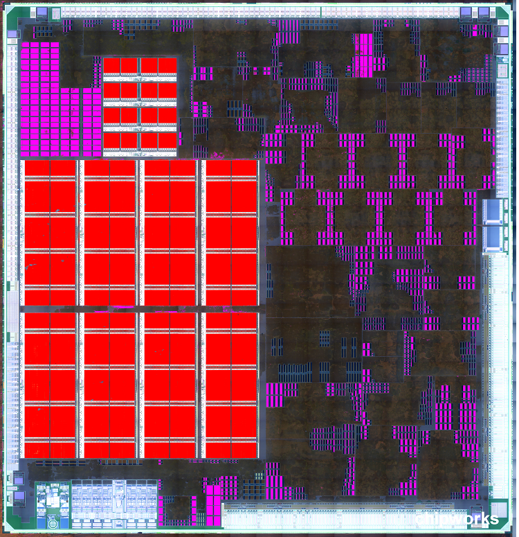
red = eDRAM
pink = L1/L2 cache
black = logic
light blue = Audio DSP
white = IO
blue = power connectors?
Green = ARM core/ PCB
red = eDRAM
pink = L1/L2 cache
black = logic
light blue = Audio DSP
white = IO
blue = power connectors?
Green = ARM core/ PCB
Some significant updates to the OP:
Here's an annotated version of the shot with some info from Randy from Chipworks:

...
Up: We just learnt from Chipworks that this kind of photo would usually cost about $2500 to do, so it really is incredibly generous of them to do it for us for free.
...
- The large orange block on the left is the 32MB of eDRAM (MEM1). Up: It's 40.72mm², and takes up 27.8% of the die. Judging by Chipworks comments above, and the densities Renesas offers for 40nm eDRAM, it is very likely at this point that the MEM1 pool of eDRAM operates with a bandwidth of 70.4GB/s.
...
Up: - The lower left units are a high-bandwidth interface such as a SERDES or MIPI. These are used to give very high bandwidth over relatively few wires, so it's likely that this is used to communicate with something elsewhere on the motherboard, possibly a chip handling compression and transfer of video to the gamepad.
Captain Smoker
Member
Great work from Chipworks again.Up: We just learnt from Chipworks that this kind of photo would usually cost about $2500 to do, so it really is incredibly generous of them to do it for us for free.
")
I don't think this is true for everyone at all. I bet people in countries where electricity is much more expensive care quite a bit.
I somehow doubt people caring that much for their electricity bill (you have to if you base you choice on a console on power consumption) would have an HDTV and a gaming console to begin with.
Absolutely. Though PPUs were a very terrible design.Sure, probably more efficient than Xenon ever was. But not much newer, or even newer at all.
And there are the inherent advantages it has over even the most bleeding edge x86 designs, of course: True RISC, 32bit, 32 registers. As far as I know, PPC750 could always address several petabytes of virtual memory, 64bit integers don't help with games at all, and while amd64 doubles the GPRs to 16, PPC750 always had 32. Add the extremely short pipeline, and I think the chip should still outperform any x86/ amd64 core clock-for-clock in many cases, even if it's a design from the last century.
faceless007
Member
When you're buying a games console. The last thing you're going to look at is it's power consumption.
You seem to be projecting your own values onto the entire consumer population. I'm not sure if anyone buys a console solely based on power ratings, but I can say that I care about heat generated and noise levels and hardware reliability, so low power does have value to me.
32 + 4 + 1, so 37MB. I guess.
If that smaller set of eDRAM is 4MB, then isn't it unlikely for that SRAM pool to the left of it to be 1MB? Since they occupy almost the same area, that would be like saying the eDRAM is 4X as dense as SRAM, even though we know real densities are closer to 3X.
On the other hand, if we say it's 3MB eDRAM + 1MB SRAM, that makes the arrangement of the eDRAM look weird. Not sure how we'd get 3MB with that arrangement(unless some of the banks are disabled? idk).
4MB for the small eDRAM does seem likely, but 1MB SRAM seems to bring densities into question. So would it make sense if the SRAM is 2MB? (128 banks.. count em and see... @ 16KB each?). This would make densities a bit more realistic, plus, breaking SRAM banks into 16KB chunks is pretty common, no?
I'm by no means a tech guy, just putting that out there for others to double-check or correct.
Some significant updates to the OP:
So what does this mean for the people that aren't that great at specs (like me)
Captain Smoker
Member
We need some kind of tech-glossary here. ^^So what does this mean for the people that aren't that great at specs (like me)
So what does this mean for the people that aren't that great at specs (like me)
lol Meelow I love you man haha
Fourth Storm
Member
Some significant updates to the OP:
Well done, Thraktor!
I should clarify that Jim from Chipworks has informed me that the CPU is very close to the interfaces on the lower left of the chip. It is very likely that the block w/ the tank oscillator facilitates a high speed low-latency connection to the CPU.
Fourth Storm
Member
Would it be too greedy to now ask for Chipworks for the same type of pics for the CPU?
They're on the way.
Schnozberry
Member
I somehow doubt people caring that much for their electricity bill (you have to if you base you choice on a console on power consumption) would have an HDTV and a gaming console to begin with.
I don't know. I think presuming either way is probably just asking to get ripped. I'm sure there are people on both sides of that argument.
Captain Smoker
Member
Awesome.They're on the way.
Up: We just learnt from Chipworks that this kind of photo would usually cost about $2500 to do, so it really is incredibly generous of them to do it for us for free.
My god... i already said this 3 times but... Thanks a ton ChipWorks.
Kaz Miirai: "2599 $!"Would it be too greedy to now ask for Chipworks for the same type of pics for the CPU?
Edit:
Wow! "Great!"They're on the way.
H_Prestige
Banned
That is indeed the most important thing to take from this. Nintendo once again cornered itself in a technological ghetto hoping that lightning would strike twice.
Yeah, it can barely handle current gen engines. Let alone next gen engines which so many experts on here were convinced it could handle.
blu
Wants the largest console games publisher to avoid Nintendo's platforms.
Which stock R7xx does that stem from?Call a lot of this 352 gflops and under 100 GB/s for edram.
ps: you do realize the edram BW is more of a speculation than the GFLOPS?
Wow, they're really being generous with all this. Big props, ChipWorks, GAF salutes you!They're on the way.
Yep. All those current gen games barely even run on the Wii U! It's a shame things are never going to get any better, developers are never going to get more used to the Wii U or any of that jazz. Wii U has already hit its maximum potential, people!Yeah, it can barely handle current gen engines.
superchunk
Member
That was the first thing I looked at when buying a 360. (Trying to snag a Jasper)
Nope. First thing were the games you wanted to play. Once you decided you wanted a 360 for its content, you then realized you didn't want one that would RROD.
Gahiggidy
My aunt & uncle run a Mom & Pop store, "The Gamecube Hut", and sold 80k WiiU within minutes of opening.
So what does this mean for the people that aren't that great at specs (like me)
lol Meelow I love you man haha
Yeah, he's right. Wtf does all that mean?
I think someone will sum it up eventually once more information is available.Zoramon089
Banned
So is it clear how much of it is there purely for BC reasons?
Not saying it can't be used for anything else (ie useless unless in Wii mode) but stuff that was put in there to make BC happen.
It was stated in the OP. 5-10% of the chip
75 Watts ? The Wii U is only using 33 Watts. If it used 75 it would be very powerful compared to current gen.
I do agree they should have inchreased it, but thats not what this thread is about. Its about determining the actual performance, not what it should have been or could have been.
this.
The work OP and company is doing is interesting. I'll wait for the conclusions.
Moral Panic
Member
What's up with the slow ass bandwidth. I thought the whole point of these split memory pools was to get bandwidths of > 200GBps but both here and the Durango we have pretty slow memory. On low-mid end PC you get video memory bandwidths 100-150GBps on much larger amounts.
Well, turns out there are two pools of eDRAM...Call a lot of this 352 gflops and under 100 GB/s for edram.
The speculated bandwidth in the OP is more than sufficient for Wii U, in terms of eDRAM.What's up with the slow ass bandwidth. I thought the whole point of these split memory pools was to get bandwidths of > 200GBps but both here and the Durango we have pretty slow memory. On PC you get video memory bandwidths 100-150GBps on much larger amounts.
This.I would like the thank ChipWorks and the GAF members who made this possible.
Can't wait to see the fully updated OP
As long as there is a caveman description at the end that goes like "wii u bad, 720 good".
Absolutely. Though PPUs were a very terrible design.
And there are the inherent advantages it has over even the most bleeding edge x86 designs, of course: True RISC, 32bit, 32 registers. As far as I know, PPC750 could always address several petabytes of virtual memory, 64bit integers don't help with games at all, and while amd64 doubles the GPRs to 16, PPC750 always had 32. Add the extremely short pipeline, and I think the chip should still outperform any x86/ amd64 core clock-for-clock in many cases, even if it's a design from the last century.
Although we're a bit off-topic here, I wrote a post on the other thread about expected DMIPS for Espresso and other gaming CPUs, and even at 1.25GHz, Espresso should perform about 35% better than Xenon in Dhrystone. Now, of course that doesn't incorporate SIMD or anything like that, but still interesting.
Well done, Thraktor!
I should clarify that Jim from Chipworks has informed me that the CPU is very close to the interfaces on the lower left of the chip. It is very likely that the block w/ the tank oscillator facilitates a high speed low-latency connection to the CPU.
That doesn't seem quite right to me. SERDES is designed to get high bandwidth out of few wires or traces. There's very little cost to running wires over an MCM (indeed that's pretty much the entire reason for the CPU and GPU being on an MCM), so a SERDES interface seems like massive overkill. On the motherboard, though, where traces are expensive (and given the use of a 64 bit memory bus, it seems Nintendo is intent on minimising the number of them), a SERDES is a sensible choice. Especially if, as Marcan apparently claimed, the actual gamepad image compression is handled on a separate chip, which means you need to transfer uncompressed video and audio across there.
Moral Panic
Member
I would like the thank ChipWorks and the GAF members who made this possible.
Can't wait to see the fully updated OP
Yeah, definitely.
I'd also add that this kind of stuff what VG journalism should be about - investigating and searching for facts to cut through rhetoric. The fact that we were only able to get this out of the kindness of Chipworks is a shame.
ambientmystic
Member
They're on the way.
Incredibly generous of Chipworks, that's like 2.5 months rent for me
phosphor112
Banned
I think it's four, not three, as there are four identical blocks, and memory macros are usually partitioned that way. The 1MB SRAM are to the left of the top eDRAM pool.
4 would make more sense I suppose, but you really think that's more SRAM up there? Why so much of all that and 3 different pools?
test_account
XP-39C²
I think it would only be an issue if another system uses 10-20 times as much power as the WiiU does, and it is being used for many hours every day. If there is only 2-3 times more power, then we're talking about saving a few dollars a month (if the systems are being used for many hours every day).I don't know. I think presuming either way is probably just asking to get ripped. I'm sure there are people on both sides of that argument.
McHuj
Member
Incredibly generous of Chipworks, that's like 2.5 months rent for me
That's awesome.
I guessing the publicity this is generating for Chipworks is worth it.
Gahiggidy
My aunt & uncle run a Mom & Pop store, "The Gamecube Hut", and sold 80k WiiU within minutes of opening.
This.
As long as there is a caveman description at the end that goes like "wii u bad, 720 good".

Fourth Storm
Member
That doesn't seem quite right to me. SERDES is designed to get high bandwidth out of few wires or traces. There's very little cost to running wires over an MCM (indeed that's pretty much the entire reason for the CPU and GPU being on an MCM), so a SERDES interface seems like massive overkill. On the motherboard, though, where traces are expensive (and given the use of a 64 bit memory bus, it seems Nintendo is intent on minimising the number of them), a SERDES is a sensible choice. Especially if, as Marcan apparently claimed, the actual gamepad image compression is handled on a separate chip, which means you need to transfer uncompressed video and audio across there.
Right, but that block is not specifically SERDES. The one to the right of it is (or MIPI). They only said it's another (but apparently different) high speed interface.
- Status
- Not open for further replies.