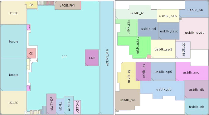
Hey folks. I have been in communication with our friends blu and bgassassin and was made aware of a link which details Brazos to some extent. I figured I'd share with you some discoveries concerning the Brazos die and what I find to be its relationship to Latte. The following is an official annotation of the Brazos made by AMD:
You can find the link
here although the rest of it is in Russian.

After racking our brains and checking against some of the Radeon documentation available online, we can confidently identify the blocks most pertinent to our discussion. Some of the acronyms may be
slightly off or incomplete, but the important thing is we have a very good idea of the blocks' functions. Going by the letters after the underscores we have:
TC=Texture Cache
TD=Texture Data
PAV=Primitive Assembly (Vertex?)
TAVC=Texture Address (Value Control? Vertex Coordinates?)
SPI_SC=Shader Processor Interpolation/Scan Converter (rasterizer)
LDS=Local Data Share
SQ=Sequencer (Ultra-threaded dispatch processor)
SX=Shader Export
CP=Command Processor
DB=Depth Buffer (ROP)
CB=Color Buffer (ROP)
Some very interesting notes come out of this.
Brazos' 4 ROPs are split into two asymmetric blocks - one for color and the other for Z/Stencil or depth. They are also located conveniently next to the DDR3 interface - just as they are on the RV770. Hey, they also look alot like the W blocks on Latte! I know I wasn't the only one to think this. Yes, the block labelled TAVC also appears similar to the W blocks, however I believe we can chalk this one up as merely a deceptive resemblance, as neither the location nor the actual amount of SRAM banks are a true match. I will defer back to the RV770 and its attested relationship to Latte in concluding that Latte's ROPs are more similar in design to the blocks in that chip. Forget about exact SRAM layout and whatnot, because as we see on Latte, even two of the same blocks on one chip can have the SRAM arranged in different ways. Thus, I would still say that Latte has 2 identical ROP blocks (so 8 ROPs total).
Most of the setup engine (minus the rasterizer) seems to lie within the block labeled PAV. I hate to say, "I told you so," but there you go. The tesselator is definitely in this block as it is shared by both the vertex and geometry setup units. After more reading, it is also clear that "Hierarchical Z" is a function of the rasterizer which checks against the depth buffer (ROP), and is not its own block. I believe the PAV block on Brazos to be a match for block G on Latte, which I have labeled as the Vertex Setup in the past. Geometry setup may be a separate block on Latte or it may not. At this point, it doesn't really matter. We know it's there.
I don't really see this, but bgassassin found some similarities between the SQ block on Brazos and Block D on Latte. I believe Block D contains the Instruction Cache and Constant Cache, both of which feed the thread dispatcher. I still think the actual UTDP is Block I, as it appears similar to something a beyond3D member labeled as thread dispatch on the Tahiti die a while back. Again, we don't really need to know for sure; the point is that we can now identify the "front end" of Latte. The Scan Converter/Rasterizer will be nearby as well. Additionally, it is quite interesting to note that even though DirectX11 hardware supposedly does away with fixed function interpolation hardware, there appears to still be something leftover of it in the spi-sc block on Brazos. Perhaps now it does not seem so ridiculous for the DirectX10.1-born Latte to feature full blown interpolation units (J Blocks).
Block C appears very similar to CP on Brazos. This is exactly where I have always expected it to be, as the command processor receives instruction from the CPU and having it adjacent to the CPU interface just makes sense. As you can see on Brazos, the command processor has a direct channel to the CPU cores.
I would still have Shader Export as Latte's Block P, as it is the only block that really qualifies. The large and somewhat messy assortment of SRAM attests to the various buffers a SX necessitates.
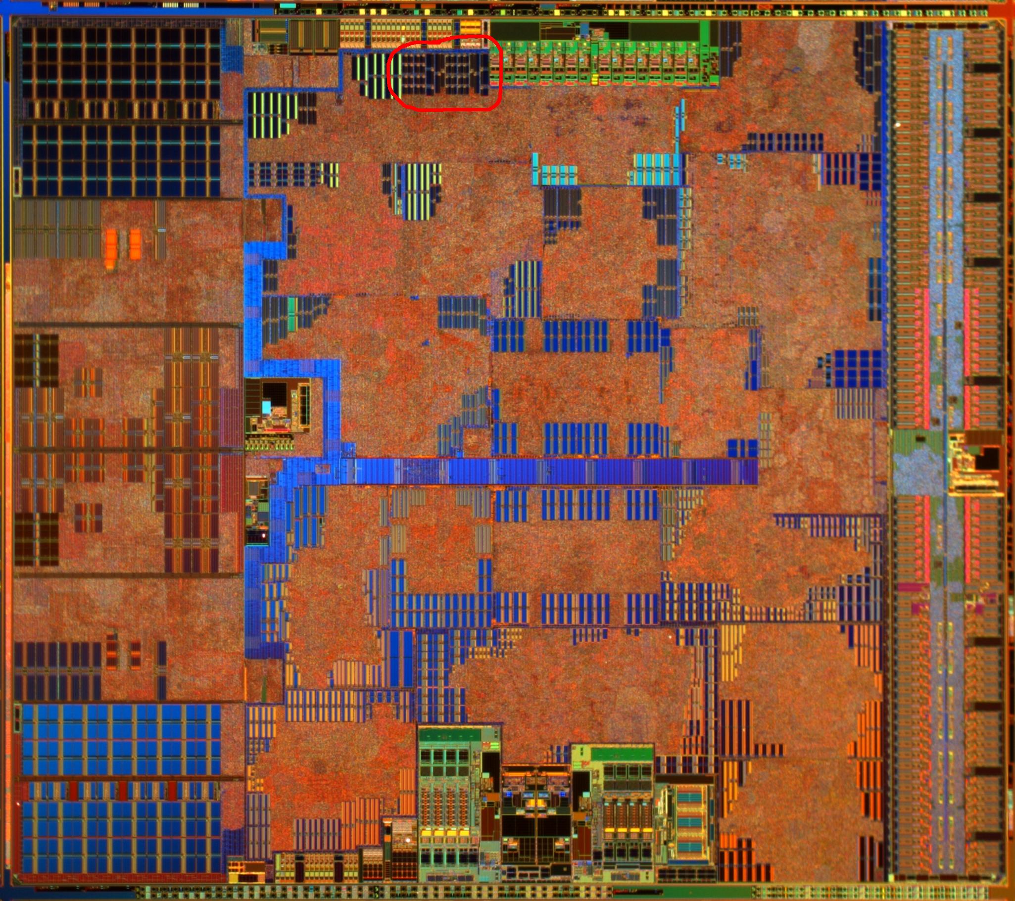
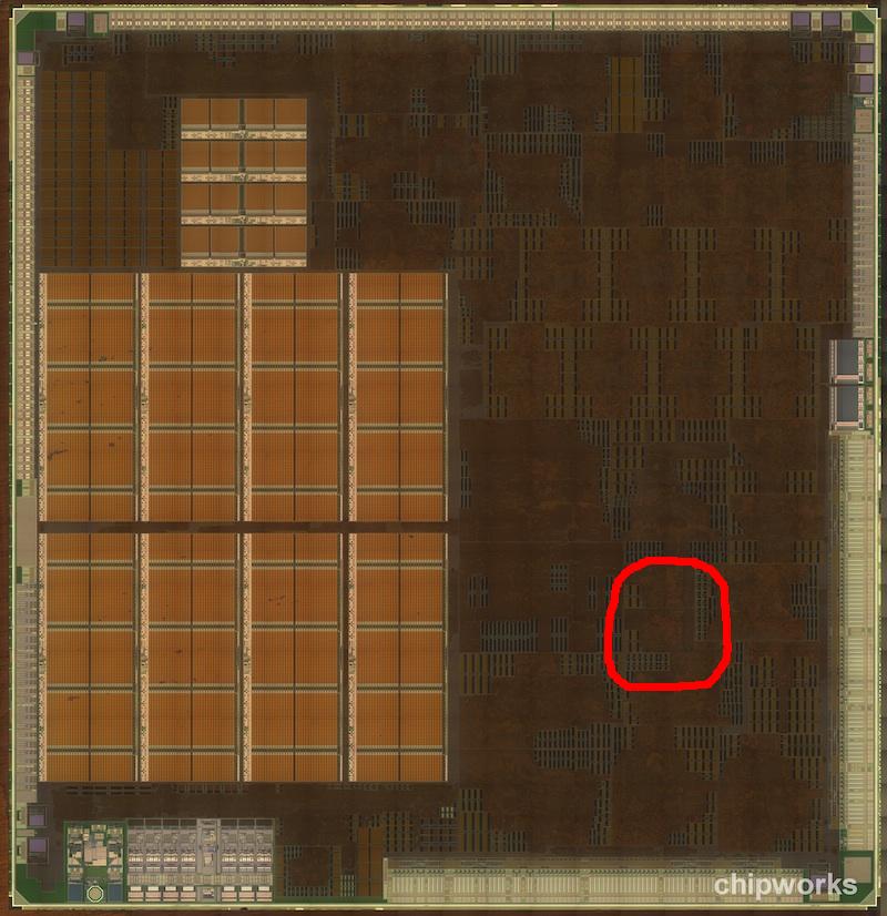
Finally, I come back to the subject of the TMUs and L1 texture cache. What I previously identified in the Llano die has once again been confirmed with the Brazos annotation. I have even used my skills at MS Paint to make it crystal clear for you all.
On Brazos, we see the same basic SRAM configuration which I previously used to link the L1s in Llano to the S Blocks in Latte. We have the 2 longer rectangular banks + a much smaller squarish bank (In Brazos, the long banks are strangely staggered, with one slightly longer as well. This is a slight variation and hardly enough to discount the similarities). Right next to these, we have the 16 other small SRAM banks. I have speculated that these might be the cache tags. Whether they are exactly this or not, it is pretty obvious that they are cache related. I bet that if we were to get a more clear picture of the RV770 die, we would see these 16 banks in the TMUs, as they are on Latte. These variations exist across the different architectures. In the Llano photo linked to in the OP, for example, those 16 banks are on the right side of the L1 blocks while the other aforementioned banks are on the left. The bottom line is that this SRAM configuration is indicative of being texture cache and TMU related. The common number of banks points directly to there being 8 TMUs on Latte, just as on Brazos.
I hope this analysis has been helpful to some. It is my opinion that from the TMU count alone we can extrapolate that Latte contains 160 shaders. Anything more would be unbalanced and nonsensical. Once we get past the hangup that the SPUs and the TMUs are not in direct contact with one another, it becomes quite easy to see that Wii U features two fairly standard SIMD engines/cores. We must give up any pretense of a dual setup engine, and it should be remembered that the only GPUs to necessitate such a configuration were absolute behemoths with many times the shading capability of even high estimates for Latte.
As for the shaders themselves,
I never claimed to have all the answers and I can't name exactly why they are so much larger than would seem to be necessary for 160 40nm SPUs. I've thrown out a few guesses in previous posts and I am sure that there have been a few modifications/shortcuts made especially for the Wii U hardware. Wsippel linked to an interesting article on thread interleaving - could be, but who knows? We could speculate forever (and that might be fun), but there's nothing else we can really say about them without actual Wii U developer insight. At this point, I don't know if I have much else to say about the Wii U GPU. I have attempted to analyze to the best of my abilities, without bias. People can believe or disbelieve as they please, just as I am sure that new game footage at E3 will have various folks claiming that the Wii U is both more and less capable than PS360. Ok, I think I'm going to go play some games now.