jeff_rigby
Banned
There have been multiple cites that stacked memory on interposer is coming for game consoles in 2013 and multiple cites for Sony interested in TSVs and stacked memory but no actual product announcement. The following in a Oct 2011 PDF published by Amkor is a product intercept for Q3 2013 for stacked DDR memory using TSVs on an Interposer with TSVs connected to CPU/GPU
AMKOR page 2 http://sites.amd.com/la/Documents/TFE2011_001AMC.pdf
AMD-Hynix Memory PDF on High Bandwidth Memory (HBM) http://sites.amd.com/us/Documents/TFE2011_006HYN.pdf. Hybrid Memory Cube (HMC) without the bottom logic layer may be identical to HBM, in principal the idea is the same but we don't know if the "standards" are the same.
Multiple professionals have been speculating this for the PS4 and at least one AMD design is getting this and I'd guess it's PS4 and Xbox 720.
Amkor is the company packaging the GF AMD APU; TSMC packages their own chips. The date on the PDF is Oct 2011 and plans to use stacked memory were already in place with the Sony CTO (Jan 2012) article and Sony lecture by SVP Technology platform (Sept 2011) both commenting on 300FPS and TSVs supporting the needed high memory bandwidth available with wide IO memory.
Sony CTO interview on Playstation tech
Compilation of Cites supporting 3D stacked memory including Sony VP Technology platform lecture with slides.
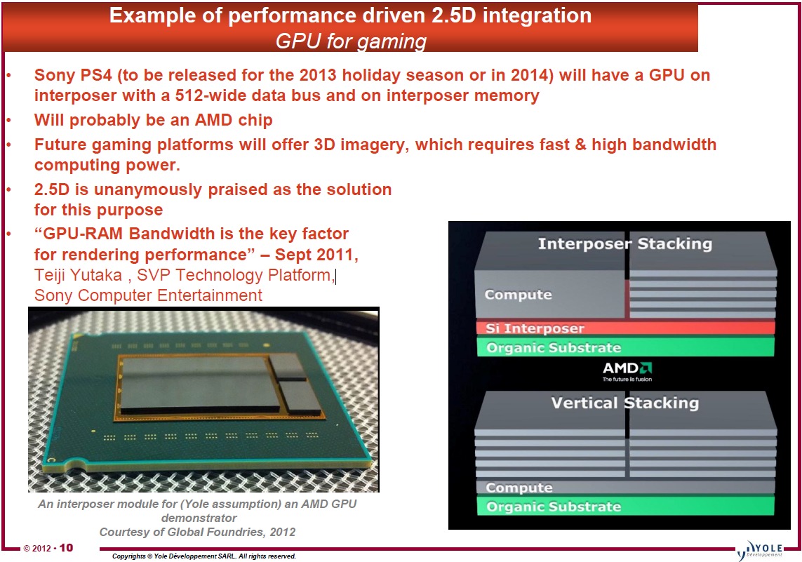
Game Console SOCs shown using 3D stacked/ultrawide with TSVs memory (faster, eventually cheaper & energy efficient) and 3D ultra wide I/O memory
Supported speculation is at least 2 Jaguar CPU packages (8 Jaguar cores) with a modified to support Wide IO GNB APU core out of the Samala/Penner APU's and a 8XXX series GPU. There may be a second GPU and it likely will be a 8XXXM series.
Delayed
From SemiAccurate uuse5
To whichever company using Amkor, could this be the confirmation of the rumors of delay for production?
PDF from Oct 2011
Page 2
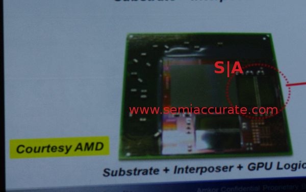
Si Interposer + DDR + Logic
GPU / CPU (28nm)
http://sites.amd.com/la/Documents/TFE2011_001AMC.pdf
PDF from Feb 2012
Page 10
http://www.amkor.com/download.cfm?d...DC8BFAE253&typename=dmFile&fieldname=filename
On page 10 we see the same chart as in the Oct 2011 document, but with Si Interposer + DDR + Logic chip delayed 6 months, pushed into mid 2014
AMKOR page 2 http://sites.amd.com/la/Documents/TFE2011_001AMC.pdf
AMD-Hynix Memory PDF on High Bandwidth Memory (HBM) http://sites.amd.com/us/Documents/TFE2011_006HYN.pdf. Hybrid Memory Cube (HMC) without the bottom logic layer may be identical to HBM, in principal the idea is the same but we don't know if the "standards" are the same.
Multiple professionals have been speculating this for the PS4 and at least one AMD design is getting this and I'd guess it's PS4 and Xbox 720.
Amkor is the company packaging the GF AMD APU; TSMC packages their own chips. The date on the PDF is Oct 2011 and plans to use stacked memory were already in place with the Sony CTO (Jan 2012) article and Sony lecture by SVP Technology platform (Sept 2011) both commenting on 300FPS and TSVs supporting the needed high memory bandwidth available with wide IO memory.
Sony CTO interview on Playstation tech
Compilation of Cites supporting 3D stacked memory including Sony VP Technology platform lecture with slides.
Game Console SOCs shown using 3D stacked/ultrawide with TSVs memory (faster, eventually cheaper & energy efficient) and 3D ultra wide I/O memory
Good news for people who wanted 2.5D stacking in nextgen consoles. We have first initial predictions about cost of silicon interposers:
http://www.electroiq.com/articles/ap/2012/12/lifting-the-veil-on-silicon-interposer-pricing.html
According to this cost analysis one 300mm silicon interposer wafer would cost $575, and this wafer could be cut into 286 blocks of 200mm2. Great price indeed, just ~2$ for 200mm2 interposer [assuming yield is 100%].
Supported speculation is at least 2 Jaguar CPU packages (8 Jaguar cores) with a modified to support Wide IO GNB APU core out of the Samala/Penner APU's and a 8XXX series GPU. There may be a second GPU and it likely will be a 8XXXM series.
Delayed
From SemiAccurate uuse5
To whichever company using Amkor, could this be the confirmation of the rumors of delay for production?
PDF from Oct 2011
Page 2
Si Interposer + DDR + Logic
GPU / CPU (28nm)
http://sites.amd.com/la/Documents/TFE2011_001AMC.pdf
PDF from Feb 2012
Page 10
http://www.amkor.com/download.cfm?d...DC8BFAE253&typename=dmFile&fieldname=filename
On page 10 we see the same chart as in the Oct 2011 document, but with Si Interposer + DDR + Logic chip delayed 6 months, pushed into mid 2014