tusharngf
Member
Could start volume production of 1.4nm chips in 2027 - 2028.
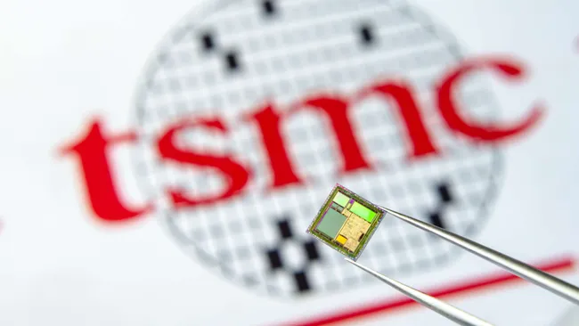
Development of TSMC's 1.4nm-class manufacturing technology is well underway, the company revealed during the Future of Logic panel during the IEEE International Electron Devices Meeting (IEDM). TSMC also re-emphasized that mass production using its 2nm-class fabrication process is on track for 2025.
TSMC's 1.4nm production node is officially called A14, according to a slide published by Dylan Patel from SemiAnalysis. For now, TSMC has not disclosed when it plans to start high-volume manufacturing (HVM) on A14 and its specifications, but with N2 scheduled for late 2025 and N2P set for late 2026, it is reasonable to guess that A14 is coming after that (2027 - 2028).
When it comes to features, A14 is unlikely to adopt vertically-stacked complementary field effect transistors (CFETs), although TSMC is exploring the technology. Therefore, A14 will probably rely on the company's 2nd or 3rd generation gate-all-around FETs (GAAFETs) — just like N2 nodes.
Nodes such as N2 and A14 will require system-level co-optimization to really make a difference and enable new levels of performance, power, and features.
What remains to be seen is whether TSMC plans to adopt High-NA EUV lithography tools for its A14 process technology in the 2027 - 2028 timeframe. Given the fact that by that time Intel (and possibly other chipmakers) will have adopted and perfected next-generation EUV litho machines with a 0.55 numerical aperture, it should be fairly easy for the contract maker of chips to use them. However, because High-NA EUV lithography tools halve reticle size, its usage will bring some additional challenges to both chip designers and chipmakers.
Source: https://www.tomshardware.com/tech-i...-for-the-first-time-says-2nm-remains-on-track
TLDR : Next gen machines will be power-efficient and expensive
