What in 2019?
Im having a hard time believing that in all honesty.
Manufacturing costs of a console are broadly defined by four things:
(i) Die-size
(ii) Thermal Design Power (or TDP)
(iii) RAM type and amount
(iv) Manufacturing yields
In designing the PS5, Sony will set for themselves constraints to design against in order to achieve a target retail price for the product; essentially these are a silicon budget (will dictate die size and directly impact things like manufacturing yields), TDP limit (i.e. maximum amount of thermal heat the console will generate and target wattage will be the considerations here - will impact costs for cooling solution and the size of the box; thus amount and type of materials used for the box) and maximum amount they're willing to spend on RAM.
After PS4's success, Sony will want to launch at the same $399 price point. So the die-size and TDP limits they determine for themselves will be similar to PS4. The performance increase over the PS4 that they can achieve will therefore be dictated by the GPU/CPU architecture they chose and how much of each they can fit within those budgets.
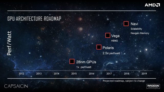
The bits that are speculative on my part, as regards the GPU SP performance specifically, are how many Navi GPU Compute Units (CUs) Sony can fit in their target APU die-size next to an 4/8 core Zen+ CPU and what is the highest clockrate at which they can set the GPU to remain within their TDP target.
We know AMD has designed Vega to run at higher clockspeeds than it's previous GCN-based architectures. Vega desktop cards (on a 16nm FF process) will reach 13+ TFLOPS this year. So if we assume Navi will continue that trend and push clocks higher on a smaller 7nm process node, then we could conceivably see a PS5 APU pushing 13-15 TFLOPs on a mature 7nm process in 2019/2020.
That's my reasoning anyway.