-
Hey, guest user. Hope you're enjoying NeoGAF! Have you considered registering for an account? Come join us and add your take to the daily discourse.
You are using an out of date browser. It may not display this or other websites correctly.
You should upgrade or use an alternative browser.
You should upgrade or use an alternative browser.
PS5 Large on-chip SRAM pool why is it being ignored?
- Thread starter onQ123
- Start date
SonGoku
Member
Quoting an old post
Post made by @gofreak about a Sony patent for SSD
TL;DR
- some hardware changes vs the typical inside the SSD (SRAM for housekeeping and data buffering instead of DRAM)
- some extra hardware and accelerators in the system for handling file IO tasks independent of the main CPU
- at the OS layer, a second file system customized for these changes
all primarily aimed at higher read performance and removing potential bottlenecks for data that is written less often than it is read, like data installed from a game disc or download.
Post made by @gofreak about a Sony patent for SSD
This will be one for people interested in some potentially more technical speculation. I posted in the next-gen speculation thread, but was encouraged to spin it off into its own thread.
I did some patent diving to see if I could dig up any likely candidates for what Sony's SSD solution might be.
I found several Japanese SIE patents from Saito Hideyuki along with a single (combined?) US application that appear to be relevant.
The patents were filed across 2015 and 2016.
Caveat: This is an illustrative embodiment in a patent application. i.e. Maybe parts of it will make it into a product, maybe all of it, maybe none of it. Approach it speculatively.
That said, it perhaps gives an idea of what Sony has been researching. And does seem in line with what Cerny talked about in terms of customisations across the stack to optimise performance.
http://www.freepatentsonline.com/y2017/0097897.html
There's quite a lot going on, but to try and break it down:
It talks about the limitations of simply using a SSD 'as is' in a games system, and a set of hardware and software stack changes to improve performance.
Basically, 'as is', an OS uses a virtual file system, designed to virtualise a host of different I/O devices with different characteristics. Various tasks of this file system typically run on the CPU - e.g. traversing file metadata, data tamper checks, data decryption, data decompression. This processing, and interruptions on the CPU, can become a bottleneck to data transfer rates from an SSD, particularly in certain contexts e.g. opening a large number of small files.
At a lower level, SSDs typically employ a data block size aimed at generic use. They distribute blocks of data around the NAND memory to distribute wear. In order to find a file, the memory controller in the SSD has to translate a request to the physical addresses of the data blocks using a look-up table. In a regular SSD, the typical data block size might require a look-up table 1GB in size for a 1TB SSD. A SSD might typically use DRAM to cache that lookup table - so the memory controller consults DRAM before being able to retrieve the data. The patent describes this as another potential bottleneck.
Here are the hardware changes the patent proposes vs a 'typical' SSD system:
- SRAM instead of DRAM inside the SSD for lower latency and higher throughput access between the flash memory controller and the address lookup data. The patent proposes using a coarser granularity of data access for data that is written once, and not re-written - e.g. game install data. This larger block size can allow for address lookup tables as small as 32KB, instead of 1GB. Data read by the memory controller can also be buffered in SRAM for ECC checks instead of DRAM (because of changes made further up the stack, described later). The patent also notes that by ditching DRAM, reduced complexity and cost may be possible, and cost will scale better with larger SSDs that would otherwise need e.g. 2GB of DRAM for 2TB of storage, and so on.
- The SSD's read unit is 'expanded and unified' for efficient read operations.
- A secondary CPU, a DMAC, and a hardware accelerator for decoding, tamper checking and decompression.
- The main CPU, the secondary CPU, the system memory controller and the IO bus are connected by a coherent bus. The patent notes that the secondary CPU can be different in instruction set etc. from the main CPU, as long as they use the same page size and are connected by a coherent bus.
- The hardware accelerator and the IO controller are connected to the IO bus.
An illustrative diagram of the system:

At a software level, the system adds a new file system, the 'File Archive API', designed primarily for write-once data like game installs. Unlike a more generic virtual file system, it's optimised for NAND data access. It sits at the interface between the application and the NAND drivers, and the hardware accelerator drivers.
The secondary CPU handles a priority on access to the SSD. When read requests are made through the File Archive API, all other read and write requests can be prohibited to maximise read throughput.
When a read request is made by the main CPU, it sends it to the secondary CPU, which splits the request into a larger number of small data accesses. It does this for two reasons - to maximise parallel use of the NAND devices and channels (the 'expanded read unit'), and to make blocks small enough to be buffered and checked inside the SSD SRAM. The metadata the secondary CPU needs to traverse is much simpler (and thus faster to process) than under a typical virtual file system.
The NAND memory controller can be flexible about what granularity of data it uses - for data requests send through the File Archive API, it uses granularities that allow the address lookup table to be stored entirely in SRAM for minimal bottlenecking. Other granularities can be used for data that needs to be rewritten more often - user save data for example. In these cases, the SRAM partially caches the lookup tables.
When the SSD has checked its retrieved data, it's sent from SSD SRAM to kernel memory in the system RAM. The hardware accelerator then uses a DMAC to read that data, do its processing, and then write it back to user memory in system RAM. The coordination of this happens with signals between the components, and not involving the main CPU. The main CPU is then finally signalled when data is ready, but is uninvolved until that point.
A diagram illustrating data flow:
Interestingly, for a patent, it describes in some detail the processing targets required of these various components in order to meet certain data transfer rates - what you would need in terms of timings from each of the secondary CPU, the memory controller and the hardware accelerator in order for them not to be a bottleneck on the NAND data speeds:
Though I wouldn't read too much into this, in most examples it talks about what you would need to support a end-to-end transfer rate of 10GB/s.
The patent is also silent on what exactly the IO bus would be - that obviously be a key bottleneck itself on transfer rates out of the NAND devices. Until we know what that is, it's hard to know what the upper end on the transfer rates could be, but it seems a host of customisations are possible to try to maximise whatever that bus will support.
Once again, this is one described embodiment. Not necessarily what the PS5 solution will look exactly like. But it is an idea of what Sony's been researching in how to customise a SSD and software stack for faster read throughput for installed game data.
I did some patent diving to see if I could dig up any likely candidates for what Sony's SSD solution might be.
I found several Japanese SIE patents from Saito Hideyuki along with a single (combined?) US application that appear to be relevant.
The patents were filed across 2015 and 2016.
Caveat: This is an illustrative embodiment in a patent application. i.e. Maybe parts of it will make it into a product, maybe all of it, maybe none of it. Approach it speculatively.
That said, it perhaps gives an idea of what Sony has been researching. And does seem in line with what Cerny talked about in terms of customisations across the stack to optimise performance.
http://www.freepatentsonline.com/y2017/0097897.html
There's quite a lot going on, but to try and break it down:
It talks about the limitations of simply using a SSD 'as is' in a games system, and a set of hardware and software stack changes to improve performance.
Basically, 'as is', an OS uses a virtual file system, designed to virtualise a host of different I/O devices with different characteristics. Various tasks of this file system typically run on the CPU - e.g. traversing file metadata, data tamper checks, data decryption, data decompression. This processing, and interruptions on the CPU, can become a bottleneck to data transfer rates from an SSD, particularly in certain contexts e.g. opening a large number of small files.
At a lower level, SSDs typically employ a data block size aimed at generic use. They distribute blocks of data around the NAND memory to distribute wear. In order to find a file, the memory controller in the SSD has to translate a request to the physical addresses of the data blocks using a look-up table. In a regular SSD, the typical data block size might require a look-up table 1GB in size for a 1TB SSD. A SSD might typically use DRAM to cache that lookup table - so the memory controller consults DRAM before being able to retrieve the data. The patent describes this as another potential bottleneck.
Here are the hardware changes the patent proposes vs a 'typical' SSD system:
- SRAM instead of DRAM inside the SSD for lower latency and higher throughput access between the flash memory controller and the address lookup data. The patent proposes using a coarser granularity of data access for data that is written once, and not re-written - e.g. game install data. This larger block size can allow for address lookup tables as small as 32KB, instead of 1GB. Data read by the memory controller can also be buffered in SRAM for ECC checks instead of DRAM (because of changes made further up the stack, described later). The patent also notes that by ditching DRAM, reduced complexity and cost may be possible, and cost will scale better with larger SSDs that would otherwise need e.g. 2GB of DRAM for 2TB of storage, and so on.
- The SSD's read unit is 'expanded and unified' for efficient read operations.
- A secondary CPU, a DMAC, and a hardware accelerator for decoding, tamper checking and decompression.
- The main CPU, the secondary CPU, the system memory controller and the IO bus are connected by a coherent bus. The patent notes that the secondary CPU can be different in instruction set etc. from the main CPU, as long as they use the same page size and are connected by a coherent bus.
- The hardware accelerator and the IO controller are connected to the IO bus.
An illustrative diagram of the system:

At a software level, the system adds a new file system, the 'File Archive API', designed primarily for write-once data like game installs. Unlike a more generic virtual file system, it's optimised for NAND data access. It sits at the interface between the application and the NAND drivers, and the hardware accelerator drivers.
The secondary CPU handles a priority on access to the SSD. When read requests are made through the File Archive API, all other read and write requests can be prohibited to maximise read throughput.
When a read request is made by the main CPU, it sends it to the secondary CPU, which splits the request into a larger number of small data accesses. It does this for two reasons - to maximise parallel use of the NAND devices and channels (the 'expanded read unit'), and to make blocks small enough to be buffered and checked inside the SSD SRAM. The metadata the secondary CPU needs to traverse is much simpler (and thus faster to process) than under a typical virtual file system.
The NAND memory controller can be flexible about what granularity of data it uses - for data requests send through the File Archive API, it uses granularities that allow the address lookup table to be stored entirely in SRAM for minimal bottlenecking. Other granularities can be used for data that needs to be rewritten more often - user save data for example. In these cases, the SRAM partially caches the lookup tables.
When the SSD has checked its retrieved data, it's sent from SSD SRAM to kernel memory in the system RAM. The hardware accelerator then uses a DMAC to read that data, do its processing, and then write it back to user memory in system RAM. The coordination of this happens with signals between the components, and not involving the main CPU. The main CPU is then finally signalled when data is ready, but is uninvolved until that point.
A diagram illustrating data flow:

Interestingly, for a patent, it describes in some detail the processing targets required of these various components in order to meet certain data transfer rates - what you would need in terms of timings from each of the secondary CPU, the memory controller and the hardware accelerator in order for them not to be a bottleneck on the NAND data speeds:

Though I wouldn't read too much into this, in most examples it talks about what you would need to support a end-to-end transfer rate of 10GB/s.
The patent is also silent on what exactly the IO bus would be - that obviously be a key bottleneck itself on transfer rates out of the NAND devices. Until we know what that is, it's hard to know what the upper end on the transfer rates could be, but it seems a host of customisations are possible to try to maximise whatever that bus will support.
Once again, this is one described embodiment. Not necessarily what the PS5 solution will look exactly like. But it is an idea of what Sony's been researching in how to customise a SSD and software stack for faster read throughput for installed game data.
- some hardware changes vs the typical inside the SSD (SRAM for housekeeping and data buffering instead of DRAM)
- some extra hardware and accelerators in the system for handling file IO tasks independent of the main CPU
- at the OS layer, a second file system customized for these changes
all primarily aimed at higher read performance and removing potential bottlenecks for data that is written less often than it is read, like data installed from a game disc or download.
Last edited:
LordKasual
Banned
Not following you on the bolder part... Xbox has it too and it is better on Xbox... because?
If it's intrinsic to the RDNA2 architecture, i'm just assuming it's bigger on Xbox and would benefit more IF Sony didn't customize specifically to increase primitive shader technology.
But i'm actually not sure where this component of the GPU is and where it fits in the graphics pipeline, so if it doesn't benefit from Xbox's higher CU count, then PS5 would actually be better at utilizing this technology because its GPU clocks significantly higher.
But i'm just speculating, i honestly don't know. Geometry Engines are relatively new in the scope of advertised features of a new GPU, so i'm not really sure how to interpret this.
I'm not speculating that it's a magic bullet for PS5, but if it's a custom feature then i can imagine it being exceedingly useful.
I Love Rock 'n' Roll
Member
This! i had to check twice to understand it!I think 99.99% of these forums posters haven't had a single clue about anything Cerny said. But here you are at every thread about PS5 trying to shit on it as fast as you can
MarkMe2525
Member
If only Sony had GTAVI as a timed exclusive like back in the PS2 days
I'll never forgive the Xbox 360 for limiting an entire generation of Grand Theft Auto because they didn't adopt the Blu-Ray (Imagine GTA IV fulfilling their original vision with the Blu-Ray/Cell Processor).
Starting price $799
Not following you on the bolder part... Xbox has it too and it is better on Xbox... because?
Geometry engine would be faster on PS5, even if its in both because the core clock is higher
Kazekage1981
Member
The tech in PS5 has been called a 'game changer' and a 'paradigm shift' by developers that have worked on it, and I think this idea is slowly starting to transpire. Series X seems much more 'standard' in terms of parts.
If the specs were reversed you would TOTALLY SAY THAT ABOUT XBOX SERIES X. Right? Riighhhhhtt? Riiiiiiiiiiiiiiiggggghhhhhhhhttttttttttt?
ethomaz
Banned
It is inside the I/O controller.That would be in the flash controller or the SSD this is on the SoC why would they take up space on the main chip for SSD RAM?
Last edited:
ethomaz
Banned
There is only one Geometry centralized unit in RDNA.If it's intrinsic to the RDNA2 architecture, i'm just assuming it's bigger on Xbox and would benefit more IF Sony didn't customize specifically to increase primitive shader technology.
But i'm actually not sure where this component of the GPU is and where it fits in the graphics pipeline, so if it doesn't benefit from Xbox's higher CU count, then PS5 would actually be better at utilizing this technology because its GPU clocks significantly higher.
But i'm just speculating, i honestly don't know. Geometry Engines are relatively new in the scope of advertised features of a new GPU, so i'm not really sure how to interpret this.
I'm not speculating that it's a magic bullet for PS5, but if it's a custom feature then i can imagine it being exceedingly useful.
So it didn’t scale with CUs.
More clocks = better performance for that unit.
Better resolution pic.
Last edited:
Neofire
Member
Yeah Ive noticed him that klickklack guy and one other popping out anti ps5 threads and sliding in and out of threads about the ps5 down playing or dismissing its features.I think 99.99% of these forums posters haven't had a single clue about anything Cerny said. But here you are at every thread about PS5 trying to shit on it as fast as you can

LordOfChaos
Member
It's part of the complex used for eliminating the SSD as a bottleneck, but in what way do you think it's not given enough attention? Seems to be on the SSD IO complex, when everyone wants to fixate on GPU ALU performance. That Sony heavily focused on the SSD is already a known quantity.
There is only one Geometry centralized unit in RDNA.
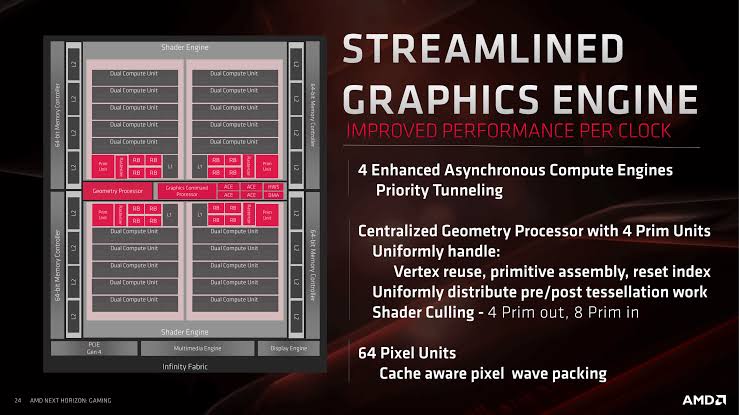
So it didn’t scale with CUs.
More clocks = better performance for that unit.
Better resolution pic.
Better image , also if Xbox SX GPU is going to get to 52(56) by having 7 Dual Compute Units in the sections where RX 5700 XT has 5 that would give PS5 the advantage for everything outside of the compute units from having the higher clock-rate but we don't know if that's the way Xbox SX GPU will be designed

Last edited:
It's part of the complex used for eliminating the SSD as a bottleneck, but in what way do you think it's not given enough attention? Seems to be on the SSD IO complex, when everyone wants to fixate on GPU ALU performance. That Sony heavily focused on the SSD is already a known quantity.
The I/O system is not just for the SSD
Clear
CliffyB's Cock Holster
Thought for you guys (further to the points I made in the "unreliable leaker" topic):
Imagine that your "source" works in QA for a major third-party publisher, and they have been working on pre-alpha builds for the latest multi-platform AAA extravaganza.
So when they tell you that the current PS5 builds run better than the equivalent XSX version, which piece of hardware would you think the more capable?
Last edited:

alabtrosMyster
Banned
On an SSD with that level of performance it should be in the vicinity of 1GB (corrected in a edit) (this is what I have on my 1TB nvme SSD).It's not being ignored; however in the grand scheme of things it's not a "large" pool of memory, either. SRAM caches almost never are. You're probably looking at 4 MB at most and it's there for things like the Coherency Engines, I/O sub-processors etc.
Last edited:
thicc_girls_are_teh_best
Member
On an SSD with that level of performance it should be in the vicinity of 1TB (this is what I have on my 1TB nvme SSD).
I'm talking about the SRAM cache; there's ZERO way the SRAM cache will be 1 TB. You will be lucky if it's 8 MB. If you're talking about the actual amount of QLC NAND on the drive, it might be 1 TB but if that were the case they could've just listed 1 TB. Partitions invisible to game and user app data for the OS files and whatnot won't take up 175+ GB.
Unless that space is reserved for OS compression like how NX Gamer was suggesting. Which would still be a massively excessive amount for such a task.
alabtrosMyster
Banned
Good point, I think you convinced him.If the specs were reversed you would TOTALLY SAY THAT ABOUT XBOX SERIES X. Right? Riighhhhhtt? Riiiiiiiiiiiiiiiggggghhhhhhhhttttttttttt?
alabtrosMyster
Banned
I meant 1GB, kike I have on my nvme drive (I corrected my post)... on the drives themselves it's common... I don't know about built-in sram memory sizes.I'm talking about the SRAM cache; there's ZERO way the SRAM cache will be 1 TB. You will be lucky if it's 8 MB. If you're talking about the actual amount of QLC NAND on the drive, it might be 1 TB but if that were the case they could've just listed 1 TB. Partitions invisible to game and user app data for the OS files and whatnot won't take up 175+ GB.
Unless that space is reserved for OS compression like how NX Gamer was suggesting. Which would still be a massively excessive amount for such a task.
LordOfChaos
Member
The I/O system is not just for the SSD
Ok, but I'm trying to understand what factor you think is being ignored, what else do you think it would do?
Ps5ProFoSho
Member
The Xbox has excited gamers. The ps5 has excited developers. I'd rather have a console with excited developers.
JareBear: Remastered
Banned
I love the concept of 'cache scrubbers', they just feel so satisfying like scrubbing that itchy part during a shower.
Also, the way Cerny explained this part on the presentation made me realize how much I wish i would've pursued software engineering.
Tell Cerny to start engineering shower scrubbers, I’ll buy three
thicc_girls_are_teh_best
Member
I meant 1GB, kike I have on my nvme drive (I corrected my post)... on the drives themselves it's common... I don't know about built-in sram memory sizes.
I think you're confusing SRAM with DRAM; most modern SSDs have a DRAM cache between 256 MB - 1 or 2 GB, depending on the size and performance level of the drive. SRAM is prohibitively more expensive than DRAM and even though that Sony SSD patent mentioned SRAM realistically it's probably only about 4 MB, 8 MB at absolute most.
Otherwise it's going to be a very expensive system and it already seems like it will be at least $450 on the MSRP (if the Japanese side won the RAM debate and they want to sell at-cost or for profit, chances are they will win on the MSRP debate too).
Azurro
Banned
It wasn't an issue with explanation, I'm sure most of us greatly understood the vast majority of the systems design and what Cerny was saying. However a lot of us also understand that he greatly embellished, that he went overboard with technical details to make things sound more impressive than they actually are.
Man, I know you are very happy of that 15-20% performance delta, but can you stop shitting every thread with your misinformation? Nothing was embellished in the presentation, and you yourself don't understand the technical details on it.
Ok, but I'm trying to understand what factor you think is being ignored, what else do you think it would do?
Besides the GPU & CPU Local cache this pool of SRAM is going to be the closet & fastest memory for the chips to use. I mostly want to know what he meant by large pool of memory , I don't think he would have called 32MB large . maybe it's 128MB or 256MB of SRAM
LordOfChaos
Member
Besides the GPU & CPU Local cache this pool of SRAM is going to be the closet & fastest memory for the chips to use. I mostly want to know what he meant by large pool of memory , I don't think he would have called 32MB large . maybe it's 128MB or 256MB of SRAM
I meant 1GB, kike I have on my nvme drive (I corrected my post)... on the drives themselves it's common... I don't know about built-in sram memory sizes.
SRAM is the most expensive memory out there, this is not DRAM like your SSD's cache.
O onQ123 I'm not sure it'll be accessible to the GPU/CPU, given the block diagram shows it's in the IO complex. If it is, a fast local scratchpad between the GPU and CPU might be interesting, but I doubt the impact will be particularly transformative (the Wii U had such a scratchpad, by the way), given the removal from the main CPU/GPU blocks and the likely sizes.
All Cerny really said about it was that all of this IO complex was meant to completely remove the storage bottleneck
Last edited:
PocoJoe
Banned
Imagine imagining that you are pointing out facts, while you are pointing digested horse food. well, maybe you dont have to imagine itImagine being offended by someone pointing out a factually based hardware hierarchy.
SRAM is the most expensive memory out there, this is not DRAM like your SSD's cache.
O onQ123 I'm not sure it'll be accessible to the GPU/CPU, given the block diagram shows it's in the IO complex. If it is, a fast local scratchpad between the GPU and CPU might be interesting, but I doubt the impact will be particularly transformative (the Wii U had such a scratchpad, by the way), given the removal from the main CPU/GPU blocks and the likely sizes.
All Cerny really said about it was that all of this IO complex was meant to completely remove the storage bottleneck
Actually when he was talking about the co-processors in the I/O he said one of them was for the SSD then when he talked about the other one he mentioned that you wouldn't typically think of that being used for the SSD but it's going to also help with the SSD. I guess that's because the SSD will also be part of the memory.
RaySoft
Member

..because there are no SRAM pool.
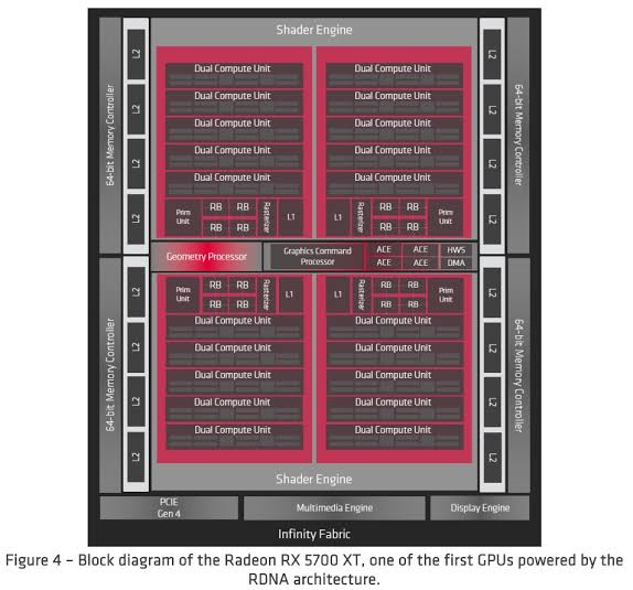
I guess you think that image is to scale?
That is just the L1 and L2 caches inside the GPU.
And oh.. Every GPU has them.
You can see them highligted here:

M1chl
Currently Gif and Meme Champion
So are we going to hype up caches? It's far more interesting to know how much of the CPU cache from Zen2 is going to be retained, because Zen2 benefits heavily thanks to big L2, L3 cache. It eleminates (to an extent) RAM timing deficiency. Which is something which GDDR memories suffer from.
SonGoku
Member
I would hope RDNA2 is more scalable than thatBetter image , also if Xbox SX GPU is going to get to 52(56) by having 7 Dual Compute Units in the sections where RX 5700 XT has 5 that would give PS5 the advantage for everything outside of the compute units from having the higher clock-rate but we don't know if that's the way Xbox SX GPU will be designed
..because there are no SRAM pool.
I guess you think that image is to scale?
That is just the L1 and L2 caches inside the GPU.
And oh.. Every GPU has them.
You can see them highligted here:
LOL are you crazy? I'm not talking about the L2 cache I'm talking about the SRAM in the I/O chip Cerny said it was a large pool of RAM
alabtrosMyster
Banned
I meant 1GB, kike I have on my nvme drive.I'm talking about the SRAM cache; there's ZERO way the SRAM cache will be 1 TB. You will be lucky if it's 8 MB. If you're talking about the actual amount of QLC NAND on the drive, it might be 1 TB but if that were the case they could've just listed 1 TB. Partitions invisible to game and user app data for the OS files and whatnot won't take up 175+ GB.
Unless that space is reserved for OS compression like how NX Gamer was suggesting. Which would still be a massively excessive amount for such a task.
Probably 8MB or a bit more of memory, just for decompression. Because decompression has to deal with many reads and writes. somewhere the data must be unpacked before it writes the "packet" to the main memory. Else the decompression-hardware would need a large chunk of the GDDR6 memory bandwidth for itself. Also sram has lower latency, so the hardware "decompressor" can achieve such high peaks like Cerny mentioned (20GB/s this should be a theoretical limit, because if the main memory is blocked a short time, the data can't be written for a while ... like every bandwidth number is highly theoretical).LOL are you crazy? I'm not talking about the L2 cache I'm talking about the SRAM in the I/O chip Cerny said it was a large pool of RAM
btw, the xbox decompression hardware should have something similar, too. But it is nothing like the sram pool from the original xbox one, where large amount of bandwidth can be saved by the GPU (which actually made everything more complicated).
ethomaz
Banned
Cerny talk about a SRAM cache they added in the I/O controller...because there are no SRAM pool.
I guess you think that image is to scale?
That is just the L1 and L2 caches inside the GPU.
And oh.. Every GPU has them.
You can see them highligted here:
Last edited:
I would hope RDNA2 is more scalable than that
More scalable than what? I haven't seen what a RDNA or RDNA2 with more than 40CUs look like but I would imagine that they would continue with the design that's broke up into 4 sections & instead of 5 dual compute units in the 4 sections they will have 7 for a total of 56CUs with 4 turned off for yielding.
Unless they will add the other CUs by going from 4 sections to 6 sections while keeping 5 dual compute units in each sections for a total of 60CUs with 8 turned off for yielding.
Probably 8MB or a bit more of memory, just for decompression. Because decompression has to deal with many reads and writes. somewhere the data must be unpacked before it writes the "packet" to the main memory. Else the decompression-hardware would need a large chunk of the GDDR6 memory bandwidth for itself. Also sram has lower latency, so the hardware "decompressor" can achieve such high peaks like Cerny mentioned (20GB/s this should be a theoretical limit, because if the main memory is blocked a short time, the data can't be written for a while ... like every bandwidth number is highly theoretical).
btw, the xbox decompression hardware should have something similar, too. But it is nothing like the sram pool from the original xbox one, where large amount of bandwidth can be saved by the GPU (which actually made everything more complicated).
I think I read it somewhere that Xbox SX will have a total of 76MB of SRAM
SonGoku
Member
I don't know how (not a graphics engineer) but if they can't increase the frontend past 40CUs it will be Vega all over again, which is garbage scalabilityMore scalable than what? I haven't seen what a RDNA or RDNA2 with more than 40CUs look like but I would imagine that they would continue with the design that's broke up into 4 sections & instead of 5 dual compute units in the 4 sections they will have 7 for a total of 56CUs with 4 turned off for yielding.
Unless they will add the other CUs by going from 4 sections to 6 sections while keeping 5 dual compute units in each sections for a total of 60CUs with 8 turned off for yielding.
Last edited:
ethomaz
Banned
But Xbox will have 52CUs so they already overcome the 40CUs limit of RDNA.I don't know how (not a graphics engineer) but if they can't increase the frontend past 40CUs it will be Vega all over again, which is garbage scalability
SonGoku
Member
Not really talking about CU limitBut Xbox will have 52CUs so they already overcome the 40CUs limit of RDNA.
One of GCN flaws was that they couldn't scale up the front end (SEs) which led to diminishing returns with the higher CU count Vega cards
ethomaz
Banned
I believe they have the same limitation with SEs yet the difference to GCN is that they have 2 arrays per SE that allowed them to have a bit more CUs per SE.Not really talking about CU limit
One of GCN flaws was that they couldn't scale up the front end (SEs) which led to diminishing returns with the higher CU count Vega cards
Said that 80CUs is the limit of RDNA... just like 64CUs was the limit for GCN.
If you look at the future of the architecture then it is really a small jump from GCN.
Last edited:
SonGoku
Member
But if they can't at least beef up those 2SEs, performance of a 80CU card will be dogshitI believe they have the same limitation with SEs yet the difference to GCN is that they have 2 arrays per SE that allowed them to have a bit more CUs per SE.
Said that 80CUs is the limit of RDNA... just like 64CUs was the limit for GCN.
If you look at the future of the architecture then it is really a small jump from GCN.
ethomaz
Banned
Well we will need to see how BigNabi works but I don’t have high hopes.But if they can't at least beef up those 2SEs, performance of a 80CU card will be dogshit
AMD says RDNA is a new generation but it still has strong roots on GCN... it is mostly a name change for marketing purposes... if RDNA was named GCN 6 it should be fine too.
Last edited:
Epic Sax CEO
Banned
Is for the IO, and you are also ignoring that the SeX have the same SRAM cache.
I don't know how (not a graphics engineer) but if they can't increase the frontend past 40CUs it will be Vega all over again, which is garbage scalability
Huh? why wouldn't it be able to go past 40CUs?
I'm not sure if we are on the same page.
Is for the IO, and you are also ignoring that the SeX have the same SRAM cache.
How would you know that? The I/O in the PS5 was designed for the PS5
ethomaz
Banned
That news for me... can you show the source for that SRAMIs for the IO, and you are also ignoring that the SeX have the same SRAM cache.
cache? The chip has basically no space for that.
Unless that pic is fake.
No SRAM cache.
Last edited:
SonGoku
Member
Perhaps i expressed myself wrongHuh? why wouldn't it be able to go past 40CUs?
I'm not sure if we are on the same page.
What im calling shit scaling is not scaling up the frontend to efficiently take advantage of the extra CUs
If the frontend remains the same between a 40CU & 80CU card, the performance of the bigger card will be limited by the frontend or in other terms diminishing returns
Similar threads
- 555
- 25K
Sneakysnake
replied