L4 cache? What/where is that in the APU?
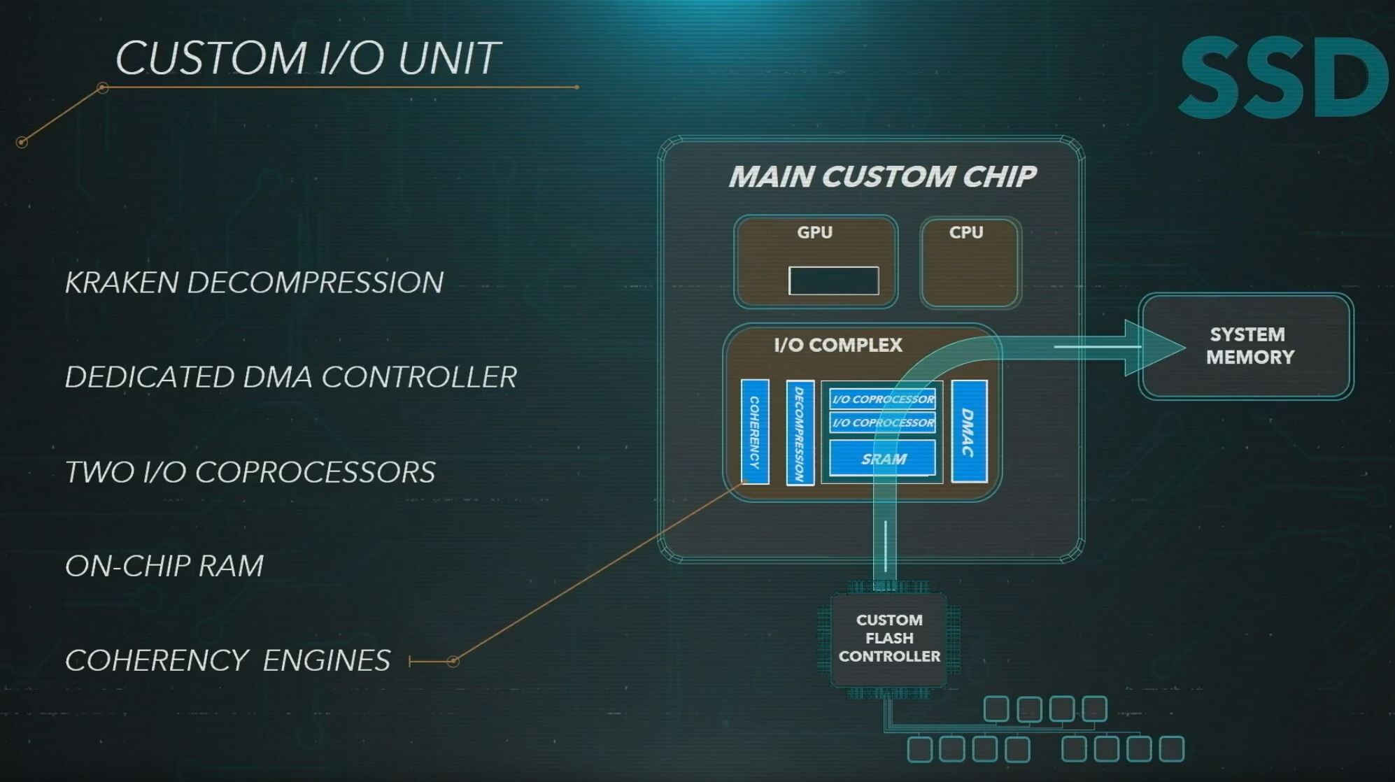
L4 cache is the embedded SRAM on the SoC. Most people probably overlooked this bit, or simply do not know what it means, but it is a static RAM that is closer to SoC than the main system 16GB GDDR6 RAM (and thus has even less latency, perfect for streaming related stuff). Don't know its size however I can speculate it is around 32-64MB. You guys probably still remember Xbox One's 32MB eSRAM that was right on the chip which was made to close the gap for their use of DDR3 RAM as main system memory instead of GDDR5. This time however, PS5 has plentiful main system RAM with good BW and really (REALLY) high bandwidth NAND chips for storage, so it is hard for me to say PS5's usage of eSRAM as it doesn't need it to increase BW but a special purpose. It takes up precious die space so the reason of its existence must be really important but don't know why people simply overlooked it. I thought it was a well known feature of PS5, certainly since it was really badly implemented in Xbox One as a stop gap for their glaring BW deficit.
Well I can speculate a few use cases:
First, Tempest Audio is configured as RAMless DMA engine so if it requires memory pointers, SRAM is closest and probably one with least latency being on the same chip.
Second, is still related to Tempest however not for audio solution for PS5 games but for BC. I think TE which is described as SPU like chip can behave like CELL for PS3, RSX is GPU portion with its own GDDR6 RAM, however you guys must remember PS3 had split memory configuration where it's GPU - RSX had its own memory and its CPU - CELL also had its own, well you guessed it; this SRAM can be the on chip CPU RAM that it needs for a PS3 BC if there was any plan of doing it. Unified memory probably would not work in hardware BC where the original console had split config. so partially it makes sense, ofc this is speculation.
Third, and this is the most possible among these, related to SFS it holds the most current virtual asset IDs for better utilization of the RAM pool and keeps from unnecessarily streaming from SSD, it is most likely that these work in tandem with new caches placed in the GPU and the scrubbers that work to partially evict these caches once they are invalidated from the list resident and live updating in the SRAM.
EDIT: So there are some people confusing SRAM in the Main SoC and the SRAM in the Custom Flash Controller chip, I will copy one of my responses here for further reading.
From the SSD patent:
http://www.freepatentsonline.com/y2017/0097897.html
"A plurality of NAND flash memories are connected to the flash memory 20. Data is stored in a distributed manner in a plurality of channels (four channels from “ch0” to “ch3” in FIG. 1) as illustrated.
The flash controller 18 includes a host controller 22, a memory controller 28, and an SRAM (Static Random Access Memory) 24."
"Thus, storing a sufficiently small-sized address conversion table in
the SRAM 24 of the flash controller 18 makes it possible to convert addresses without the mediation of an external DRAM."
Fig. 4 at
http://www.freepatentsonline.com/20170097897.pdf
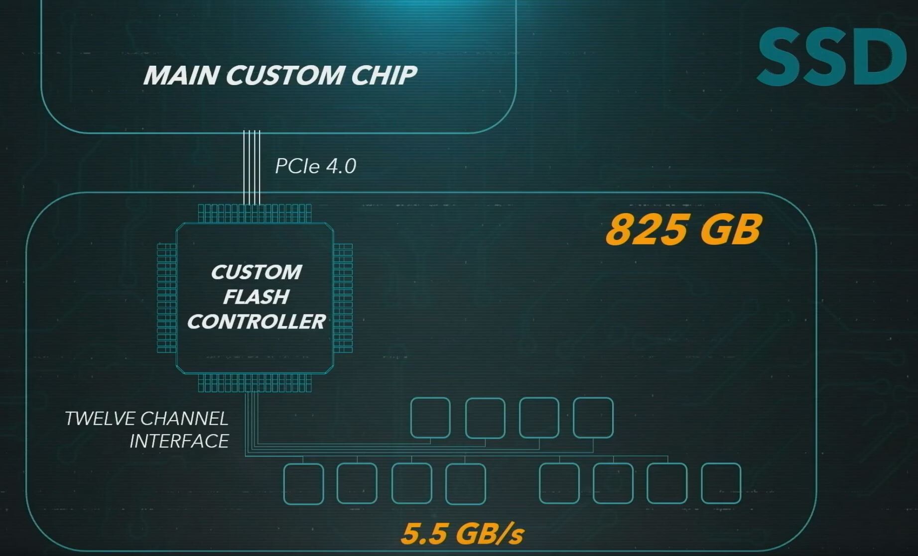
That unit is 'Custom Flash Controller' pictured here
>>> There is SRAM in that Unit AS WELL AS a different SRAM in the Main SoC that has different purpose. NAND chips require RAM very close at hand and SRAM that is inside the 'Custom Flash Controller' provides that. eSRAM that is inside the SoC is comparatively far away, and it is embedded right on the die of SoC which has different purpose.
The SRAM mentioned in the patent refers to one that is inside 'Custom Flash Controller' Unit. So there is SRAM in the Main Chip - SoC and there is ALSO another SRAM on the Custom Flash Controller, mainly for residing lookup tables, do not mix the two just because the names are the same, SRAM. The one inside the SoC is actually eSRAM as in embedded SRAM that has different purpose than arbitration of physical address space of game install/save file locations etc.