BlacknGold_Blood
Member
Yes, Epic did confirm that was not done for loading purposes.I would have to look for a source but apparently the small gap in the Epic demo was an artistic decision to show how good the textures was.
Yes, Epic did confirm that was not done for loading purposes.I would have to look for a source but apparently the small gap in the Epic demo was an artistic decision to show how good the textures was.
L4 cache is the embedded SRAM on the SoC. Most people probably overlooked this bit, or simply do not know what it means, but it is a static RAM that is closer to SoC than the main system 16GB GDDR6 RAM (and thus has even less latency, perfect for streaming related stuff). Don't know its size however I can speculate it is around 32-64MB. You guys probably still remember Xbox One's 32MB eSRAM that was right on the chip which was made to close the gap for their use of DDR3 RAM as main system memory instead of GDDR5. This time however, PS5 has plentiful main system RAM with good BW and really (REALLY) high bandwidth NAND chips for storage, so it is hard for me to say PS5's usage of eSRAM as it doesn't need it to increase BW but a special purpose. It takes up precious die space so the reason of its existence must be really important but don't know why people simply overlooked it. I thought it was a well known feature of PS5, certainly since it was really badly implemented in Xbox One as a stop gap for their glaring BW deficit.
Well I can speculate a few use cases:
First, Tempest Audio is configured as RAMless DMA engine so if it requires memory pointers, SRAM is closest and probably one with least latency being on the same chip.
Second, is still related to Tempest however not for audio solution for PS5 games but for BC. I think TE which is described as SPU like chip can behave like CELL for PS3, RSX is GPU portion with its own GDDR6 RAM, however you guys must remember PS3 had split memory configuration where it's GPU - RSX had its own memory and its CPU - CELL also had its own, well you guessed it; this SRAM can be the on chip CPU RAM that it needs for a PS3 BC if there was any plan of doing it. Unified memory probably would not work in hardware BC where the original console had split config. so partially it makes sense, ofc this is speculation.
Third, and this is the most possible among these, related to SFS it holds the most current virtual asset IDs for better utilization of the RAM pool and keeps from unnecessarily streaming from SSD, it is most likely that these work in tandem with new caches placed in the GPU and the scrubbers that work to partially evict these caches once they are invalidated from the list resident and live updating in the SRAM.
From the PS5 devkit patent the other day, one of the diagrams shows the SoC location IIRC, I suspect rough dimensions could be ascertained from that. Worst case, it should show the upper limit of the expected SoC they'd ever intend to use.That is 32 MB of embedded SRAM on Xbox One SoC. As you can see it is divided into two chunks of 16MBs. Those are as big as 14 Xbox One AMD GCN Compute Units. It was the main reason why Xbox could only fit in 14 GCN CUs into the SoC and thus much less powerful in terms of TFLOPs.
Now for PS5 it is completely different. 2TF power deficit and fitting just 36 RDNA2 CUs (which are around 60% larger than PS4 GCN CUs) is only making 18% difference AND that is with fitting SRAM into the SoC along with everything I/O related.
With these in mind, I think PS5 SoC die size is not smaller than XSX SoC, it is either very close, or actually as I suspect more and more it is really bigger than it. The secrecy surrounding the teardown and the fact that we haven't seen not even an engineering sample leak images or any kind of digital render of the SoC in any promotional materials really gives credence to the speculation that PS5 actually has a bigger die than XSX.
Xbox version comes with exclusive elevators and hallways!!
I can't see there being news today. They'll wait a "respectful" amount of time after Mr Floyd's funeral and that is on the 9th.
We might hear a murmur in the evening (US time) of the 10th if things are calm enough. They might even wait until 11.
I do think the 12th is a possible date for it though, it just might be short notice.
Where are you getting that info from - hopefully not github? And what is the PS5 devkits solution for debugging - if they don't have twice the retail unit's memory to be able to observe without interfering?Not without adding more memory controllers onto the APU. As far as I know, PS5 has 4 x 64bit(lanes) controllers, the 8 x 2GB GDDR6 RAM chips are 32 lanes. So 2 RAM modules are connected per memory controller... or if the 4GB ram modules are available then yeah
I'm predicting that those rumors/comments of the Series X and PS5 being released outside November will be true. Series X in September, PS5 in October to avoid competition during Christmas time.
I have a feeling the recession (at least in the US) will play a factor whether or not people will divert their money to other things this year. For many, a Console will be a much lesser priority if they haven't worked for nearly half the year.
Well what we know so far is that at first no one would believe next-gen consoles would have a 12TF GPU. That was followed by Sony showing the tech behind their amazingly fast SSD. On one side they say it changes the game, on the other side they say it won't be that much of a difference, in both cases (GPU/SSD). Fans just quote whatever fits their narrative, and we still haven't seen actual games.
in·spired
/inˈspī(ə)rd/
Learn to pronounce
adjective
1. of extraordinary quality, as if arising from some external creative impulse.
"they had to thank the goalie for some inspired saves"
rev·o·lu·tion·ar·y
/ˌrevəˈlo͞oSHəˌnerē/
Learn to pronounce
adjective
1. involving or causing a complete or dramatic change.
"a revolutionary new drug"
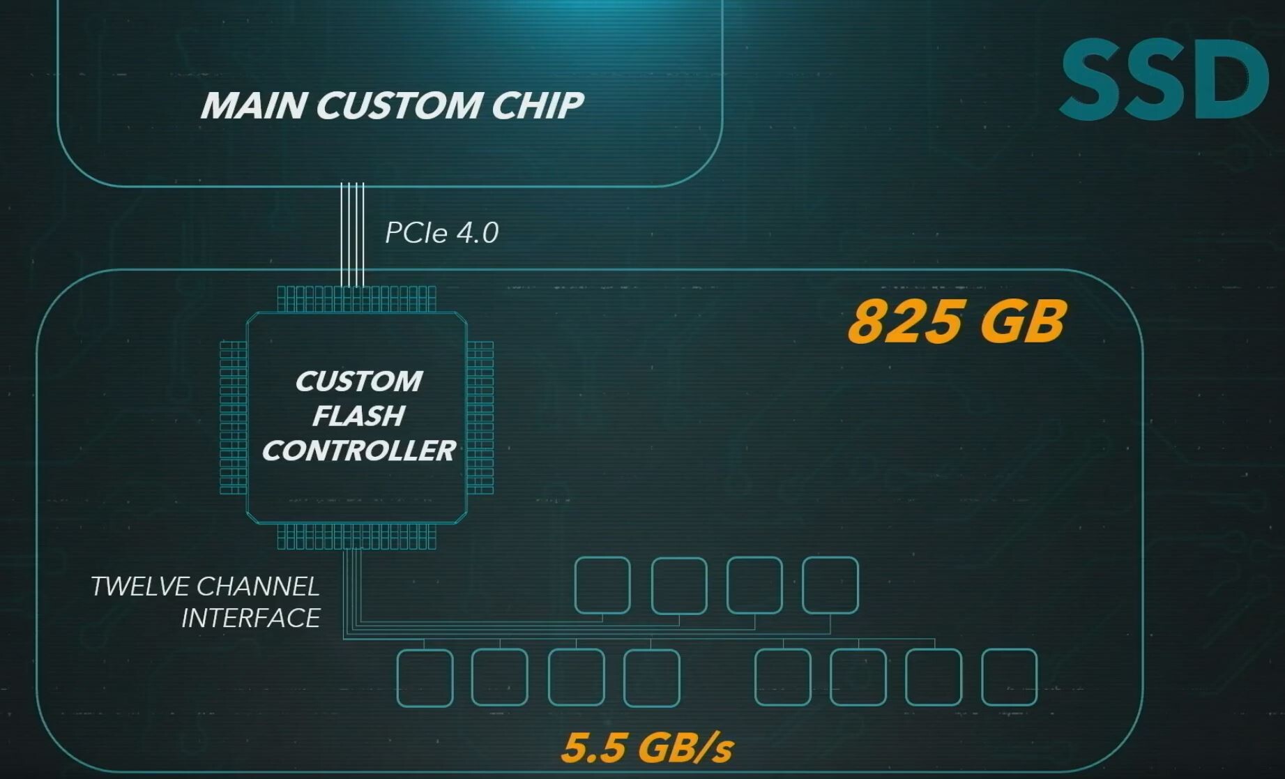
```A plurality of NAND flash memories are connected to the flash memory 20. Data is stored in a distributed manner in a plurality of channels (four channels from “ch0” to “ch3” in FIG. 1) as illustrated. The flash controller 18 includes a host controller 22, a memory controller 28, and an SRAM (Static Random Access Memory) 24.```I’m not sure I understand this because I read a brief explanation on ResetEra of the patent that Cerny’s SSD and I/O implementation are based off of and it sounded like the SRAM pool on the main custom chip only serves one purpose that’s related to file I/O. I may be wrong on this but here’s the link to the thread:

PS5 - a patent dive into what might be the tech behind Sony's SSD customisations (technical!)
This will be one for people interested in some potentially more technical speculation. I posted in the next-gen speculation thread, but was encouraged to spin it off into its own thread. I did some patent diving to see if I could dig up any likely candidates for what Sony's SSD solution might...www.resetera.com
This is pretty big, as he is a current MS dev and he is speaking on camera so it is what it is.
Maybe on that EPIC demo the walk through the small gap and the bloom when the ceiling opens is to allow non Ps5 hardware to load stuff and not have to stream per frame ?

The correct response to ad hominem." #PS5 fans need to get over themselves, pronto!"
I think the only certainty we have is there'll be at least an update this week, no way they can keep radio silence till next Monday.I can't see there being news today. They'll wait a "respectful" amount of time after Mr Floyd's funeral and that is on the 9th.
We might hear a murmur in the evening (US time) of the 10th if things are calm enough. They might even wait until 11.
I do think the 12th is a possible date for it though, it just might be short notice.
I'm inclined to say this as well. I wouldn't be surprised to see an earlier launch, but these are very tumultuous times, both socially and economically.
It makes you wonder if they really will indeed be $500, because that is a big chunk of change no matter what, but far moreso in the worst recession in a long time.
I also expect both to be very limited quantities. But the way 2020 has gone, I wouldn't be surprised if more unfortunate events occur that causes(or forces) them both to slip into 2021. Sometimes, I just think that's a wiser move. This year has been rough 6 months in AND its an election year also.
I think the only certainty we have is there'll be at least an update this week, no way they can keep radio silence till next Monday.
Look above ^^.The SRAM in the IO Complex is used for decoding, decrypting and decompressing data from kernel memory into user memory according to the Sony storage architecture patent.
It isn’t a generic cache, and it’s not even accessed by the CPU but by a coprocessor and the decompressor.
 www.freepatentsonline.com
The patent is AFAIK did not have calling or any indication of the sizes being scaled to the real, they are just design figures I doubt they are in real scale.From the PS5 devkit patent the other day, one of the diagrams shows the SoC location IIRC, I suspect rough dimensions could be ascertained from that. Worst case, it should show the upper limit of the expected SoC they'd ever intend to use.
The cancelled PS5 event for the 6th might have shown the chip by then, so it is also possible the patent sizes are engineering sizes.
Two different chips will use a different amount of power at the same clock speed.
Raising clockspeed will always increase power consumption.
https://physics.stackexchange.com/q...h-the-processor-frequency-in-a-typical-comput
..unless they are not active but then well, there would the advantage go if they were (are not).That's what got me thinking about a higher price and a bump in memory size for the PS5. There seems little point in subsidising an expensive console in a global recession (IMHO). Better to add value and charge at a profit so that those that can afford it at launch price buy it while seeing the value.I'm predicting that those rumors/comments of the Series X and PS5 being released outside November will be true. Series X in September, PS5 in October to avoid competition during Christmas time.
I have a feeling the recession (at least in the US) will play a factor whether or not people will divert their money to other things this year. For many, a Console will be a much lesser priority if they haven't worked for nearly half the year.
what election, why it should matter for consoles ?I'm inclined to say this as well. I wouldn't be surprised to see an earlier launch, but these are very tumultuous times, both socially and economically.
It makes you wonder if they really will indeed be $500, because that is a big chunk of change no matter what, but far moreso in the worst recession in a long time.
I also expect both to be very limited quantities. But the way 2020 has gone, I wouldn't be surprised if more unfortunate events occur that causes(or forces) them both to slip into 2021. Sometimes, I just think that's a wiser move. This year has been rough 6 months in AND its an election year also.
" #PS5 fans need to get over themselves, pronto!"
Good Morning!!! These images are circulating on the #MediaMarkt website, which were instantly deleted.
It is usually the “Modus Operandi” before a presentation. The names of "PS5 turbo" or "CPU Gonzalo" are enclave names, not their final name. # PlayStation5 is very close
The patent is AFAIK did not have calling or any indication of the sizes being scaled to the real, they are just design figures I doubt they are in real scale.
Well yea, everyone else moved on because Sony disappointed with a 10 TF machine.
Boy! am I glad to see you again!4pm BST is my prediction for today.
The picture is a placeholder, but the price is interesting (499 €).
The picture is a placeholder, but the price is interesting (499 €).
$500 during these times would be alot for many if they haven't saved, for sure. That Lockhart potentially being $299 could be a great thing for Microsoft. However, I saw that Cyberpunk limited edition pre-orders already sold out and that's $399. I guess if people really want something, they'll get it.
The picture is a placeholder, but the price is interesting (499 €).
 www.mediamarkt.es
Look above ^^.
"A plurality of NAND flash memories are connected to the flash memory 20. Data is stored in a distributed manner in a plurality of channels (four channels from “ch0” to “ch3” in FIG. 1) as illustrated. The flash controller 18 includes a host controller 22, a memory controller 28, and an SRAM (Static Random Access Memory) 24.INFORMATION PROCESSING DEVICE, ACCESS CONTROLLER, INFORMATION PROCESSING METHOD, AND COMPUTER PROGRAM - Sony Interactive Entertainment Inc.
<div p-id="p-0001">Disclosed herein is an information processing device including a host unit adapted to request data access by specifying a logical address of a secondary storage device, and a contro
"Thus, storing a sufficiently small-sized address conversion table in the SRAM 24 of the flash controller 18 makes it possible to convert addresses without the mediation of an external DRAM."
Fig. 4 at http://www.freepatentsonline.com/20170097897.pdf
That unit is 'Custom Flash Controller' pictured here
There is SRAM in that Unit AS WELL AS a different SRAM in the Main SoC that has different purpose. NAND chips require RAM very close at hand and SRAM that is inside the 'Custom Flash Controller' provides that. eSRAM that is inside the SoC is comparatively far away, and it is embedded right on the die of SoC which has different purpose.
Sony hasn't sold me on a $500 console yet. I am more likely to wait for 1 to 2 years and then upgrade my launch PS4 . Sony needs to show me games at launch which justify the early investment in the PS5/SDD. The UE5 demo was great but UE5 will not be launched until next year so we likely won't see a title which uses it for a year or more later. I also wasn't really happy with the whole mid-gen refresh they did last gen. So if there is a chance of another one this gen I may just wait until the refresh to buy in . Maybe the reveal will swing me over... lets see.
GT7 is going to be eye candy. Cannot wait!!!!Yeah that info was posted last week from that Chinese Article regarding the production. At this point I just want to see the games and get a release date.
4pm BST is my prediction for today.
This is pretty big, as he is a current MS dev and he is speaking on camera so it is what it is.
Maybe on that EPIC demo the walk through the small gap and the bloom when the ceiling opens is to allow non Ps5 hardware to load stuff and not have to stream per frame ?
Not sure how true this is but it won’t surprise me.
Xbox version comes with exclusive elevators and hallways!!
Even so we don't know the size of the real devkit to compare the scale to, and even then the SoC is in mm2 which would be nigh impossible to calculate some estimate of its area by looking at a scale of something that you don't know the real size.The only thing that makes it feel like it is derived from a scaled engineering diagram (IMO) is that it has a lot of parts that need to line up, and the V shape plates that lock together might look less representative if the other parts aren't scaled accordingly. The exterior looked correctly proportioned, so the internals would surely need to be proportioned correctly. But you are probably correct, I bet they have a patents department to obfuscate dimensions/info to avoid revealing product details before a reveal.
Would love an exact quote from the patent file, of "The purpose of the pool of SRAM in the IO Complex--the SRAM I was referring to--is explained further along in the patent documentation." instead of trust me I've read this more than you and thus know it by heart. Put money where your mouth is and show the receipts like I did or I'm unconvinced.Sorry, Apollo, but I have read perhaps a bit more of this patent than you have. I know there are (at least) two pools of SRAM involved in Sony's IO solution, and have in fact pointed this out myself in this thread.
The purpose of the pool of SRAM in the IO Complex--the SRAM I was referring to--is explained further along in the patent documentation. You've found that the flash controller uses it too, which is another innovation, but the pool in the IO Complex--according to the patent at least--is to assist the co-processor in decrypting, decompressing etc.
No indication at all that it's a generic cache, and I can't see how that could work with the storage pipeline constantly needing access to it.
Isn't this even more confirmation that - for multiplatform games - developers will not actually use the PS5 SSD to its fullest?
I mean, think about it, if the developers would built their multiplatform games around the PS5 SSD, they would have to basically create two version of a game.
One Version for PS5 and one version for XSX and PCs with SSD.
Would this - from economic point of view- feasible?
I think not, we are not going to see anything like this. I think what we will see is the following:
Developers will build their games around the PC SSD and use as the lowest common denominator and then XSX and PS5 will benefit from shorter loading times compared to PC, but other than that, it won't be different to PC.
It simply isn't feasible at all, developing games is already super expensive and developing a game version for PS5 and one for XSX/PC would make it even more expensive.
Of course, this doesn't apply to CPU and GPU.
With CPU and GPU it's very easy to scale up and down, we have seen this in current gen and on PC, where we have different modes and settings, e.g. lower or higher FPS/Resolution. This is super easy and doesn't take any resources from the developers, the developer doesn't have to create different versions of a game.
Isn't this even more confirmation that - for multiplatform games - developers will not actually use the PS5 SSD to its fullest?
Isn't this even more confirmation that - for multiplatform games - developers will not actually use the PS5 SSD to its fullest?
I mean, think about it, if the developers would built their multiplatform games around the PS5 SSD, they would have to basically create two version of a game.
One Version for PS5 and one version for XSX and PCs with SSD.
Would this - from economic point of view- feasible?
I think not, we are not going to see anything like this. I think what we will see is the following:
Developers will build their games around the PC SSD and use as the lowest common denominator and then XSX and PS5 will benefit from shorter loading times compared to PC, but other than that, it won't be different to PC.
It simply isn't feasible at all, developing games is already super expensive and developing a game version for PS5 and one for XSX/PC would make it even more expensive.
Of course, this doesn't apply to CPU and GPU.
With CPU and GPU it's very easy to scale up and down, we have seen this in current gen and on PC, where we have different modes and settings, e.g. lower or higher FPS/Resolution. This is super easy and doesn't take any resources from the developers, the developer doesn't have to create different versions of a game.
No one is disappointed with 10.3 TF console, the PS5’s SSD will be able to create worlds and stream assets in/out that no other console can do, so Sony exclusives have to be dumbed-down to be able to run on Xbox Series X.Well yea, everyone else moved on because Sony disappointed with a 10 TF machine.