El Sueño
Member
You should get a kid. Mine is seven and I can say Roblox is massive. He plays a lot when he is allowed to.I have no ideia what Roblox is or even existed.
You should get a kid. Mine is seven and I can say Roblox is massive. He plays a lot when he is allowed to.I have no ideia what Roblox is or even existed.
yes, 18% more theoretical compute performanceSX has at least 18% more compute or RTX performance over PS5.I do not think there can be any doubt in this. Having said that PS5 might have less bottleneck and better API that is why there is no serious advantage of one over the other.
yes, 18% more theoretical compute performance
First, that theoretical figure only happens on paper, as unless you're crypto mining, no software will use 100% of those CUs.
Second of all, 18% more compute does not equal 18% more performance in games, which is what I was explaining. It may well perform worse, depending on the game (as we've seen already btw).

SX has at least 18% more compute or RTX performance over PS5.I do not think there can be any doubt in this. Having said that PS5 might have less bottleneck and better API that is why there is no serious advantage of one over the other.
Can it be like this:Clockspeed do matter but still SX has 18% more due to more CU. Microsoft in Hot chips presentation stated that SX can do 380 billion ray intersection per sec. 4*52*1.825ghz = 379.6. So the PS5 should be 4*36*2.23ghz = 321.12. Which is 18% less.
Wow. You speak like only MS has a theoretical peak. Underscores and everything, huh?
Wow. You speak like only MS has a theoretical peak. Underscores and everything, huh?
")
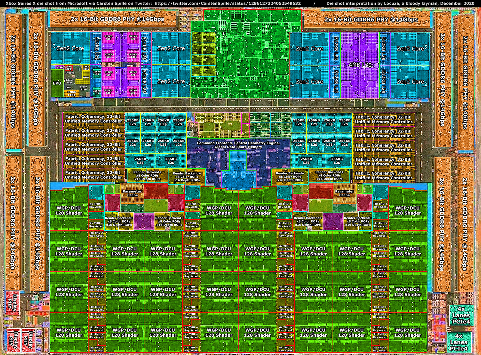
I made a die shot analysis video for the Xbox Series X and S chips though the first part is just limited to the I/O:
It may be interesting for some, especially since all sources are in the description box and I lay down how you can figure out different hardware blocks.
So to some extend it's like a tutorial and you can learn how to analyse die shots yourself.
However you need some background knowledge and not everything will be easy to follow if you are just a casual hardware enthusiast.
That said some may not like to watch videos or can't, so here is a small summary:
1.) When companies share the die sizes it's not always clear what they mean by that.
Sometimes they mean the whole chip size, sometimes just the chip design itself, without the scribe line.
In some cases the official die size doesn't fit either way, so the first thing you should do, when you want to measure structure sizes, is to check on the die sizes yourself.
https://abload.de/img/mega-leaks-part-5-xboyyjr3.png
2.) First a short CPU analysis of the Zen2 Matisse (CPU) and Renoir (APU) die shots.
They both share the same CPU core sizes of 2.83mm² and the structures look basically identical, so AMD uses the same design libraries and physical implementation.
https://abload.de/img/mega-leaks-part-5-xbok9jvo.png
3.) AMD only changed the L3$ design, reducing the capacity from 16MiB (CPU) to 4MiB (APU).The CCX size goes down from 31.37mm² to 20.21mm².
A Renoir CCX is 11.16mm² smaller.
You could get 3x 4MB CCXes (3x 20.21mm = 60.63mm²) for the price of 2x 16MB CCXes (2x 31.37mm² = 62.74mm²).
It's more than obvious why there is a large motivation in cutting down the L3$ if area is important.
https://abload.de/img/mega-leaks-part-5-xbo5ojye.png
4.) In the past I made a hypothetical CCX mockup with 8MB per CCX, resulting in ~24.23mm².
It was an interesting question what Renoir, the Xbox Series and PS5 would use (was still open back then).
Now it's known that Renoir, Xbox Series and PS5 all use 4MB for the L3$ per CCX. https://abload.de/img/mega-leaks-part-5-xboeckzt.png
5.) The assumption now is of course that the Xbox Series and PS5 use the same Renoir design and implementation (which is not true for the PS5 as we know).
Comparing the Xbox Series CCXes to AMD's Zen2 CCXes shows basically the same picture, at least the size should be identical.
https://abload.de/img/mega-leaks-part-5-xboh9j0c.pnghttps://abload.de/img/mega-leaks-part-5-xborkk9d.png
Because of the low resolution it's hard to tell if some digital logic is not laid down differently, on the FPU and L3$ side there appear to be some differences but I wouldn't make the call right now.
6.) The core size on the Xbox Series should be identical with 2.83mm², meaning the die shot MS shared at Hot Chips is 372.16mm², larger than the final chips.
https://abload.de/img/mega-leaks-part-5-xbo07jqp.png
7.) Thanks to the XSX teardown on ifixit we can say that the final chips are ~360mm² in size, as MS officially stated with 360.45mm².
The chip design itself is ~354.71mm² large on XSX and 192.18mm² on the XSS.
https://pbs.twimg.com/media/Ew2ziieWgAsA8Z8?format=jpg&name=large
https://abload.de/img/mega-leaks-part-5-xboeakmw.png
https://abload.de/img/mega-leaks-part-5-xbonrjsg.png
8.) For time reasons I just managed to include the I/O sections, where MS is stating 5 I/O blocks, 3 on the left and two on the right side.
We obviously want to know what they are for.
Looking at them makes it clear that we have two different types of I/O.
Based on official information we only have 3 major I/O connections; Display, 8x PCIe4 Lanes and GDDR6 links.
2x PCIe4 lanes are used for the internal and 2x for the external SSD.
The Southbridge is a dedicated chip which is also attached via the PCIe standard and contains USB3 interfaces, a system controller, SPI, etc.
So one I/O type should be for display and the other for PCIe.
The left I/O blocks don't fit to 4 display links or 8 PCIe4 lanes.
But the right I/O blocks have 4 yellow stripes and if those are PCIe Lanes that would fit perfectly to 8 PCIe4 Lanes.
https://abload.de/img/mega-leaks-part-5-xboz6khw.png
9.) We can check that simple assumption thanks to Fritzchens Fritz, who has die shots of Navi10 and Navi14 on his flickr account.
Comparing the I/O sections and other analog elements shows basically no differences, outside of two larger blocks colored in red and cyan.
N10 has 6 red blocks, N14 just 5.
N10 has 4 cyan blocks, N14 just 2.
https://abload.de/img/mega-leaks-part-5-xboickrc.png
10.) The cyan blocks look identical to the right I/O blocks on the Xbox Series X and they share the exact same size.
There is only one major I/O specification which could come into question here.
N10 has 16x PCIe4 lanes, while N14 only has 8x PCIe4 Lanes.
We can conclude that the cyan blocks are PHYs for PCIe4 and that each yellow stripe is a single lane:
https://abload.de/img/mega-leaks-part-5-xbomrjd7.png
11.) Finding the display specifications per GPU is not so easy, I think you really have to look at the open source drivers to find the information about how many display controllers are present per GPU.
N10 has 6, N14 5, which fits to the red blocks which look very similar to the left I/O blocks on Xbox Series.
https://abload.de/img/mega-leaks-part-5-xbo9sjo5.png
12.) Why the Xbox Series X has 3 of those (display) I/O PHYs is still a mystery to me, the Xbox Series S just has 1.
https://pbs.twimg.com/media/Ew25RAQWQAAtdwX?format=jpg&name=large
13.) One could also look at the traces on the PCB to figure out the I/O situation but for a layperson this is not always presenting a clear picture.
https://abload.de/img/mega-leaks-part-5-xboeckfu.png
14.) Finally the GDDR6 I/O, which MS officially annotated but they would have been easy to make out anyway.
DRAM PHYs are usually the largest interfaces on a chip and in most cases there are no other options which fit to the memory specifications.
For example the Xbox Series X has a 320-Bit wide interface and each GDDR6 memory chip is connected via 32-Bits, meaning that the PHY needs to fit to the number 10 in some way.
Either we should see 5 larger blocks, 10 or 20 but not something which is not part of that number series.
On the Xbox Series X we see exactly 10 larger I/O PHYs around the chip edges.
In addition I made just a visual representation how the 10GB of "GPU Optimal Memory" should be in principle mapped over the full 320-Bit Interface and how the 6GB "Standard Memory" is addressed over 192-Bits/6 memory chips.
https://abload.de/img/mega-leaks-part-5-xbodekll.png
https://abload.de/img/mega-leaks-part-5-xboy7jki.png
https://abload.de/img/mega-leaks-part-5-xbo83kyk.png
------
In the end we should roughly come up with this picture (yellow TMU blocks are part of the WGPs and the green/cyan blocks on the left and right side from the Parameter Cache should relate to the Primitive Units and Rasterizer):
Full res and with other information here:
One interesting point may relate to the CCXes:
The PS5 CPU has some cut downs on the FPU side (at least the FP register file was reduced), making the CCX shorter than on the Xbox Series and AMD's Zen2 CPUs.
?Both TF counts are theoretical. It's just some systems get closer to those numbers on average than others. This can help explain why 10TFs and 12TFs seem pretty close when on paper the difference should be a lot bigger.
But how much RAM is available for Devs on PS5, we still don't know officially and I wonder if we ever will.It's not the bandwidth that matters most and remember Xbox one had sram so it minimised the bandwidth problem and a faster cpu, the reason games looked similar on PS4 and xbone was because they both had 8gb ram, the reason PS3 an for x360 games looked similar was because they both had 512mb ram. Ram is always king in graphics it's everything you first have to fit whatever your rendering all your data sets in your memory budgets then everything else can be scalled down.
But the series s has 10gb while ps5/x have 16gb this completely kills developers, you can go watch every documentary or talk of game developers and memory is all they talk about infact it's the culprit in 90 percent of the games it's the reason cyberpunk is a Mess on lastgen consoles it's why theres stutters, missing assets there wasn't enough memory same thing that killed PS3 and x360 in their last days pcs had already been having 2gb gpus and games needed more memory.
Consoles have fixed budgets of memory unlike pcs you can have a 6gb gpu and 16gb system ram so when the game runs out of gpu ram it starts using system ram and because system ram is slower so you'll just get popin and lower fps but on console it's different you have fixed 10gb on series s about 7.5gb only is usable for games and you have no escape that's your budget and to make a game that was natively made for ps5/x to run properly on series s will take a lot of time so what devs do in the end is make it for the weaker console series s and then easily port to ps5/x but this will make the game suffer because you could have made it more spectacular if you natively made it to run on more memory on ps5 and x so another way is to forget about series s just make a game for ps5/x then do a cheap mess on series s. And that's what I think devs will do in the end.
I made a die shot analysis video for the Xbox Series X and S chips, though the first part is just limited to the I/O:
It may be interesting for some, especially since all sources are in the description box and I lay down how you can figure out different hardware blocks.
So to some extend it's like a tutorial and you can learn how to analyse die shots yourself.
However you need some background knowledge and not everything will be easy to follow if you are just a casual hardware enthusiast.
That said some may not like to watch videos or can't, so here is a small summary:
1.) When companies share the die sizes it's not always clear what they mean by that.
Sometimes they mean the whole chip size, sometimes just the chip design itself, without the scribe line.
In some cases the official die size doesn't fit either way, so the first thing you should do, when you want to measure structure sizes, is to check on the die sizes yourself.
https://abload.de/img/mega-leaks-part-5-xboyyjr3.png
2.) First a short CPU analysis of the Zen2 Matisse (CPU) and Renoir (APU) die shots.
They both share the same CPU core sizes of 2.83mm² and the structures look basically identical, so AMD uses the same design libraries and physical implementation.
https://abload.de/img/mega-leaks-part-5-xbok9jvo.png
3.) AMD only changed the L3$ design, reducing the capacity from 16MiB (CPU) to 4MiB (APU).The CCX size goes down from 31.37mm² to 20.21mm².
A Renoir CCX is 11.16mm² smaller.
You could get 3x 4MB CCXes (3x 20.21mm = 60.63mm²) for the price of 2x 16MB CCXes (2x 31.37mm² = 62.74mm²).
It's more than obvious why there is a large motivation in cutting down the L3$ if area is important.
https://abload.de/img/mega-leaks-part-5-xbo5ojye.png
4.) In the past I made a hypothetical CCX mockup with 8MB per CCX, resulting in ~24.23mm².
It was an interesting question what Renoir, the Xbox Series and PS5 would use (was still open back then).
Now it's known that Renoir, Xbox Series and PS5 all use 4MB for the L3$ per CCX. https://abload.de/img/mega-leaks-part-5-xboeckzt.png
5.) The assumption now is of course that the Xbox Series and PS5 use the same Renoir design and implementation (which is not true for the PS5 as we know).
Comparing the Xbox Series CCXes to AMD's Zen2 CCXes shows basically the same picture, at least the size should be identical.
https://abload.de/img/mega-leaks-part-5-xboh9j0c.pnghttps://abload.de/img/mega-leaks-part-5-xborkk9d.png
Because of the low resolution it's hard to tell if some digital logic is not laid down differently, on the FPU and L3$ side there appear to be some differences but I wouldn't make the call right now.
6.) The core size on the Xbox Series should be identical with 2.83mm², meaning the die shot MS shared at Hot Chips is 372.16mm², larger than the final chips.
https://abload.de/img/mega-leaks-part-5-xbo07jqp.png
7.) Thanks to the XSX teardown on ifixit we can say that the final chips are ~360mm² in size, as MS officially stated with 360.45mm².
The chip design itself is ~354.71mm² large on XSX and 192.18mm² on the XSS.
https://pbs.twimg.com/media/Ew2ziieWgAsA8Z8?format=jpg&name=large
https://abload.de/img/mega-leaks-part-5-xboeakmw.png
https://abload.de/img/mega-leaks-part-5-xbonrjsg.png
8.) For time reasons I just managed to include the I/O sections, where MS is stating 5 I/O blocks, 3 on the left and two on the right side.
We obviously want to know what they are for.
Looking at them makes it clear that we have two different types of I/O.
Based on official information we only have 3 major I/O connections; Display, 8x PCIe4 Lanes and GDDR6 links.
2x PCIe4 lanes are used for the internal and 2x for the external SSD.
The Southbridge is a dedicated chip which is also attached via the PCIe standard and contains USB3 interfaces, a system controller, SPI, etc.
So one I/O type should be for display and the other for PCIe.
The left I/O blocks don't fit to 4 display links or 8 PCIe4 lanes.
But the right I/O blocks have 4 yellow stripes and if those are PCIe Lanes that would fit perfectly to 8 PCIe4 Lanes.
https://abload.de/img/mega-leaks-part-5-xboz6khw.png
9.) We can check that simple assumption thanks to Fritzchens Fritz, who has die shots of Navi10 and Navi14 on his flickr account.
Comparing the I/O sections and other analog elements shows basically no differences, outside of two larger blocks colored in red and cyan.
N10 has 6 red blocks, N14 just 5.
N10 has 4 cyan blocks, N14 just 2.
https://abload.de/img/mega-leaks-part-5-xboickrc.png
10.) The cyan blocks look identical to the right I/O blocks on the Xbox Series X and they share the exact same size.
There is only one major I/O specification which could come into question here.
N10 has 16x PCIe4 lanes, while N14 only has 8x PCIe4 Lanes.
We can conclude that the cyan blocks are PHYs for PCIe4 and that each yellow stripe is a single lane:
https://abload.de/img/mega-leaks-part-5-xbomrjd7.png
11.) Finding the display specifications per GPU is not so easy, I think you really have to look at the open source drivers to find the information about how many display controllers are present per GPU.
N10 has 6, N14 5, which fits to the red blocks which look very similar to the left I/O blocks on Xbox Series.
https://abload.de/img/mega-leaks-part-5-xbo9sjo5.png
12.) Why the Xbox Series X has 3 of those (display) I/O PHYs is still a mystery to me, the Xbox Series S just has 1.
https://pbs.twimg.com/media/Ew25RAQWQAAtdwX?format=jpg&name=large
13.) One could also look at the traces on the PCB to figure out the I/O situation but for a layperson this is not always presenting a clear picture.
https://abload.de/img/mega-leaks-part-5-xboeckfu.png
14.) Finally the GDDR6 I/O, which MS officially annotated but they would have been easy to make out anyway.
DRAM PHYs are usually the largest interfaces on a chip and in most cases there are no other options which fit to the memory specifications.
For example the Xbox Series X has a 320-Bit wide interface and each GDDR6 memory chip is connected via 32-Bits, meaning that the PHY needs to fit to the number 10 in some way.
Either we should see 5 larger blocks, 10 or 20 but not something which is not part of that number series.
On the Xbox Series X we see exactly 10 larger I/O PHYs around the chip edges.
In addition I made just a visual representation how the 10GB of "GPU Optimal Memory" should be in principle mapped over the full 320-Bit Interface and how the 6GB "Standard Memory" is addressed over 192-Bits/6 memory chips.
https://abload.de/img/mega-leaks-part-5-xbodekll.png
https://abload.de/img/mega-leaks-part-5-xboy7jki.png
https://abload.de/img/mega-leaks-part-5-xbo83kyk.png
------
In the end we should roughly come up with this picture (yellow TMU blocks are part of the WGPs and the green/cyan blocks on the left and right side from the Parameter Cache should relate to the Primitive Units and Rasterizer):
Full res and with other information here:
One interesting point may relate to the CCXes:
The PS5 CPU has some cut downs on the FPU side (at least the FP register file was reduced), making the CCX shorter than on the Xbox Series and AMD's Zen2 CPUs.
____
Any feedback, questions or answers are welcomed.
No. Not at all.If you go by paper specifications the differences should be bigger than what we are seeing. How close each system can get to their maximums can help explain that.
No. Not at all.
You are seeing what you want to see, in my previous example I mentioned PC hardware to explain why tflops does not equate gaming performance.Wow. You speak like only MS has a theoretical peak. Underscores and everything, huh?
I made a die shot analysis video for the Xbox Series X and S chips, though the first part is just limited to the I/O:
It may be interesting for some, especially since all sources are in the description box and I lay down how you can figure out different hardware blocks.
So to some extend it's like a tutorial and you can learn how to analyse die shots yourself.
However you need some background knowledge and not everything will be easy to follow if you are just a casual hardware enthusiast.
That said some may not like to watch videos or can't, so here is a small summary:
1.) When companies share the die sizes it's not always clear what they mean by that.
Sometimes they mean the whole chip size, sometimes just the chip design itself, without the scribe line.
In some cases the official die size doesn't fit either way, so the first thing you should do, when you want to measure structure sizes, is to check on the die sizes yourself.
https://abload.de/img/mega-leaks-part-5-xboyyjr3.png
2.) First a short CPU analysis of the Zen2 Matisse (CPU) and Renoir (APU) die shots.
They both share the same CPU core sizes of 2.83mm² and the structures look basically identical, so AMD uses the same design libraries and physical implementation.
https://abload.de/img/mega-leaks-part-5-xbok9jvo.png
3.) AMD only changed the L3$ design, reducing the capacity from 16MiB (CPU) to 4MiB (APU).The CCX size goes down from 31.37mm² to 20.21mm².
A Renoir CCX is 11.16mm² smaller.
You could get 3x 4MB CCXes (3x 20.21mm = 60.63mm²) for the price of 2x 16MB CCXes (2x 31.37mm² = 62.74mm²).
It's more than obvious why there is a large motivation in cutting down the L3$ if area is important.
https://abload.de/img/mega-leaks-part-5-xbo5ojye.png
4.) In the past I made a hypothetical CCX mockup with 8MB per CCX, resulting in ~24.23mm².
It was an interesting question what Renoir, the Xbox Series and PS5 would use (was still open back then).
Now it's known that Renoir, Xbox Series and PS5 all use 4MB for the L3$ per CCX. https://abload.de/img/mega-leaks-part-5-xboeckzt.png
5.) The assumption now is of course that the Xbox Series and PS5 use the same Renoir design and implementation (which is not true for the PS5 as we know).
Comparing the Xbox Series CCXes to AMD's Zen2 CCXes shows basically the same picture, at least the size should be identical.
https://abload.de/img/mega-leaks-part-5-xboh9j0c.pnghttps://abload.de/img/mega-leaks-part-5-xborkk9d.png
Because of the low resolution it's hard to tell if some digital logic is not laid down differently, on the FPU and L3$ side there appear to be some differences but I wouldn't make the call right now.
6.) The core size on the Xbox Series should be identical with 2.83mm², meaning the die shot MS shared at Hot Chips is 372.16mm², larger than the final chips.
https://abload.de/img/mega-leaks-part-5-xbo07jqp.png
7.) Thanks to the XSX teardown on ifixit we can say that the final chips are ~360mm² in size, as MS officially stated with 360.45mm².
The chip design itself is ~354.71mm² large on XSX and 192.18mm² on the XSS.
https://pbs.twimg.com/media/Ew2ziieWgAsA8Z8?format=jpg&name=large
https://abload.de/img/mega-leaks-part-5-xboeakmw.png
https://abload.de/img/mega-leaks-part-5-xbonrjsg.png
8.) For time reasons I just managed to include the I/O sections, where MS is stating 5 I/O blocks, 3 on the left and two on the right side.
We obviously want to know what they are for.
Looking at them makes it clear that we have two different types of I/O.
Based on official information we only have 3 major I/O connections; Display, 8x PCIe4 Lanes and GDDR6 links.
2x PCIe4 lanes are used for the internal and 2x for the external SSD.
The Southbridge is a dedicated chip which is also attached via the PCIe standard and contains USB3 interfaces, a system controller, SPI, etc.
So one I/O type should be for display and the other for PCIe.
The left I/O blocks don't fit to 4 display links or 8 PCIe4 lanes.
But the right I/O blocks have 4 yellow stripes and if those are PCIe Lanes that would fit perfectly to 8 PCIe4 Lanes.
https://abload.de/img/mega-leaks-part-5-xboz6khw.png
9.) We can check that simple assumption thanks to Fritzchens Fritz, who has die shots of Navi10 and Navi14 on his flickr account.
Comparing the I/O sections and other analog elements shows basically no differences, outside of two larger blocks colored in red and cyan.
N10 has 6 red blocks, N14 just 5.
N10 has 4 cyan blocks, N14 just 2.
https://abload.de/img/mega-leaks-part-5-xboickrc.png
10.) The cyan blocks look identical to the right I/O blocks on the Xbox Series X and they share the exact same size.
There is only one major I/O specification which could come into question here.
N10 has 16x PCIe4 lanes, while N14 only has 8x PCIe4 Lanes.
We can conclude that the cyan blocks are PHYs for PCIe4 and that each yellow stripe is a single lane:
https://abload.de/img/mega-leaks-part-5-xbomrjd7.png
11.) Finding the display specifications per GPU is not so easy, I think you really have to look at the open source drivers to find the information about how many display controllers are present per GPU.
N10 has 6, N14 5, which fits to the red blocks which look very similar to the left I/O blocks on Xbox Series.
https://abload.de/img/mega-leaks-part-5-xbo9sjo5.png
12.) Why the Xbox Series X has 3 of those (display) I/O PHYs is still a mystery to me, the Xbox Series S just has 1.
https://pbs.twimg.com/media/Ew25RAQWQAAtdwX?format=jpg&name=large
13.) One could also look at the traces on the PCB to figure out the I/O situation but for a layperson this is not always presenting a clear picture.
https://abload.de/img/mega-leaks-part-5-xboeckfu.png
14.) Finally the GDDR6 I/O, which MS officially annotated but they would have been easy to make out anyway.
DRAM PHYs are usually the largest interfaces on a chip and in most cases there are no other options which fit to the memory specifications.
For example the Xbox Series X has a 320-Bit wide interface and each GDDR6 memory chip is connected via 32-Bits, meaning that the PHY needs to fit to the number 10 in some way.
Either we should see 5 larger blocks, 10 or 20 but not something which is not part of that number series.
On the Xbox Series X we see exactly 10 larger I/O PHYs around the chip edges.
In addition I made just a visual representation how the 10GB of "GPU Optimal Memory" should be in principle mapped over the full 320-Bit Interface and how the 6GB "Standard Memory" is addressed over 192-Bits/6 memory chips.
https://abload.de/img/mega-leaks-part-5-xbodekll.png
https://abload.de/img/mega-leaks-part-5-xboy7jki.png
https://abload.de/img/mega-leaks-part-5-xbo83kyk.png
------
In the end we should roughly come up with this picture (yellow TMU blocks are part of the WGPs and the green/cyan blocks on the left and right side from the Parameter Cache should relate to the Primitive Units and Rasterizer):
Full res and with other information here:
One interesting point may relate to the CCXes:
The PS5 CPU has some cut downs on the FPU side (at least the FP register file was reduced), making the CCX shorter than on the Xbox Series and AMD's Zen2 CPUs.
____
Any feedback, questions or answers are welcomed.

Could be more considering the ssd has 512mb aswell could be anything from 14-15gb is my guess but that wouldnt be a big problem for series x 13.5gb it just means multi platform games will target 13.5gb as base and ps5 io as base depending if the game requires ssd streaming like open world games! This wont be an issue on pc since nobody cares about pcs. Youll have to deal with popin on other machines.But how much RAM is available for Devs on PS5, we still don't know officially and I wonder if we ever will.
There's no such thing as a 2 TF difference, it doesn't mean anything. That's MS marketing, I know, but machines don't actually work like that, tons of devs explained that already. TF are theorical peak number of instructions per second, it's meaningless in real life. You never reach this number. Then there's cache, system clock, I/O, memory bandwidth, hardware customizations of all sorts... All those have nothing to do with teraflops.What I'm saying is that I'm not seeing a 2TF kind of a difference in these games.
Do you claim to have an innate knowledge of what a '2TF kind of difference' looks like in games? By the way humble advice, let this TF obsession go, or else it will be groundhog day until the end of the generation.What I'm saying is that I'm not seeing a 2TF kind of a difference in these games.
Some people were saying an 1800P vs 4K kind of a difference would be standard.Do you claim to have an innate knowledge of what a '2TF kind of difference' looks like in games? By the way humble advice, let this TF obsession go, or else it will be groundhog day until the end of the generation.
Clockspeed do matter but still SX has 18% more due to more CU. Microsoft in Hot chips presentation stated that SX can do 380 billion ray intersection per sec. 4*52*1.825ghz = 379.6. So the PS5 should be 4*36*2.23ghz = 321.12. Which is 18% less.
Someone once said "you have to feed those CUs with work" and "it's easier to do it with a higher clock".
I can't quite remember who said that...

Someone once said "you have to feed those CUs with work" and "it's easier to do it with a higher clock".
I can't quite remember who said that...

The funny thing is that a simple 1 hour presentation by Mark Cerney keeps on giving. It's incredible how much you can just quote it and the discussion kinda ends there
Shots fired.
The funny thing is that a simple 1 hour presentation by Mark Cerney keeps on giving. It's incredible how much you can just quote it and the discussion kinda ends there
I mean Sony hasn't said anything else on the hardware but that one hour video!
I mean, we werent actually meant to even see the Road to PS5 on youtube at all IIRC, it was meant for GDC. I have a hard time of thinking of it in ”marketing”-terms. Marketing for devs maybe, but It was clearly not aimed at casual viewers, even if it turned out that way.Some people brushed it off as marketing BS but some of what he said did come true. I'm curious to see what will happen once developers take full advantage of the PS5 once they get used to the tools.
Yeah, but I am so incredibly happy that they did it anyhow. I get it that it was too technical for a lot of people, but for me it was very informative and I actually found it a bit too simplistic.I mean, we werent actually meant to even see the Road to PS5 on youtube at all IIRC, it was meant for GDC. I have a hard time of thinking of it in ”marketing”-terms. Marketing for devs maybe, but It was clearly not aimed at casual viewers, even if it turned out that way.
The next video will explain how PS5 has the oldest RDNA 1.0 ROPS ever and how the machine was put together with spare parts obtained from ancient Akkadian graves.So the PS5 has older ROPs, not RNDA2 correct me if I'm wrong, cheers
I mean, we werent actually meant to even see the Road to PS5 on youtube at all IIRC, it was meant for GDC. I have a hard time of thinking of it in ”marketing”-terms. Marketing for devs maybe, but It was clearly not aimed at casual viewers, even if it turned out that way.


 www.vgchartz.com
I liked it as well, watched it live when it aired. I get what you mean by it being slightly too simplistic though. Microsoft has been very open about pretty much every single thing inside the Series X, while Sony has stayed much more tight-lipped. This has worked in Microsofts favour, at least in these types of forums.Yeah, but I am so incredibly happy that they did it anyhow. I get it that it was too technical for a lot of people, but for me it was very informative and I actually found it a bit too simplistic.
PS5 vs Xbox Series X|S vs Switch Launch Sales Comparison Through Week 17 - Sales
PS5 Vs. Xbox Series X|S Vs. Switch Global:
Through the first 17 weeks available worldwide the PlayStation 5 is ahead of the Switch and Xbox Series X|S by a fair margin. The PS5 is ahead of the Switch by 1.98 million units and is 2.13 million units ahead of the Xbox Series X|S. The Switch is ahead of the Xbox Series X|S by only 131,189 units.
- PS5: 6,078,333
- Switch: 4,096,742
- XSX|S: 3,944,563
The PS5 has sold 6.08 million in 17 weeks worldwide, while the Switch sold 4.10 million units and the Xbox Series X|S 3.94 million units.
Looking at the marketshare through 17 weeks, the PlayStation 5 currently leads. The PS5 has a 43.1 percent marketshare, the Switch sits at 29.0 percent, and the Xbox Series X|S at 27.9 percent.
The Switch didn't reach current PS5 sales until week 30.
PS5 vs Xbox Series X|S vs Switch Launch Sales Comparison Through Week 17
This weekly mini-series compares the aligned launch sales of the PlayStation 5, Xbox Series X|S, and Nintendo Switch. It [...]
I liked it as well, watched it live when it aired. I get what you mean by it being slightly too simplistic though. Microsoft has been very open about pretty much every single thing inside the Series X, while Sony has stayed much more tight-lipped. This has worked in Microsofts favour, at least in these types of forums.
The next video will explain how PS5 has the oldest RDNA 1.0 ROPS ever and how the machine was put together with spare parts obtained from ancient Akkadian graves.
PS5 vs Xbox Series X|S vs Switch Launch Sales Comparison Through Week 17 - Sales
PS5 Vs. Xbox Series X|S Vs. Switch Global:
Through the first 17 weeks available worldwide the PlayStation 5 is ahead of the Switch and Xbox Series X|S by a fair margin. The PS5 is ahead of the Switch by 1.98 million units and is 2.13 million units ahead of the Xbox Series X|S. The Switch is ahead of the Xbox Series X|S by only 131,189 units.
- PS5: 6,078,333
- Switch: 4,096,742
- XSX|S: 3,944,563
The PS5 has sold 6.08 million in 17 weeks worldwide, while the Switch sold 4.10 million units and the Xbox Series X|S 3.94 million units.
Looking at the marketshare through 17 weeks, the PlayStation 5 currently leads. The PS5 has a 43.1 percent marketshare, the Switch sits at 29.0 percent, and the Xbox Series X|S at 27.9 percent.
The Switch didn't reach current PS5 sales until week 30.
PS5 vs Xbox Series X|S vs Switch Launch Sales Comparison Through Week 17
This weekly mini-series compares the aligned launch sales of the PlayStation 5, Xbox Series X|S, and Nintendo Switch. It [...]
I liked it as well, watched it live when it aired. I get what you mean by it being slightly too simplistic though. Microsoft has been very open about pretty much every single thing inside the Series X, while Sony has stayed much more tight-lipped. This has worked in Microsofts favour, at least in these types of forums.
I already feel not so good about posting the video in this thread, self-promotion and such.Make a thread about it, it's shame to do such great work and let it be here.
There might be some changes done, based on what was on RDNA1 GPUs but the ROP configuration appears to be the same as on RDNA1.So the PS5 has older ROPs, not RNDA2 correct me if I'm wrong, cheers
Seriously though, the PS5 appears to use IP which is even older than on RDNA1 GPUs from AMD.The next video will explain how PS5 has the oldest RDNA 1.0 ROPS ever and how the machine was put together with spare parts obtained from ancient Akkadian graves.
Finally been waiting for someone to do this.
____
Any feedback, questions or answers are welcomed.
Older, but there are actually bigger and better. PS5 has cut down FPU (CPU), but XSX has actually cut-down ROPs (GPU).So the PS5 has older ROPs, not RNDA2 correct me if I'm wrong, cheers
The main thing I got from this was the XSX ram situation and the PCIe setup.So the PS5 has older ROPs, not RNDA2 correct me if I'm wrong, cheers
I already feel not so good about posting the video in this thread, self-promotion and such.
I may ask for a greenlight from a mod first.
There might be some changes done, based on what was on RDNA1 GPUs but the ROP configuration appears to be the same as on RDNA1.
Xbox Series uses the RB configuration found on RDNA2.
Now with configuration I mean how the ROPs are configured on a high level and not that they are exactly the same.
However by and large I would assume that the ROPs on the PS5 are mostly comparable to RDNA1 ROPs and the ROPs on the XS to ROPs on RDNA2 with HW support for Variable Rate Shading.
Seriously though, the PS5 appears to use IP which is even older than on RDNA1 GPUs from AMD.
Indicating that Sony and AMD worked very early on this project.
However also new features such as RT are included, showing how flexible and granular the hw can be mixed and changed.
The Switch didn't launch during a pandemic with isolation measures though.PS5 vs Xbox Series X|S vs Switch Launch Sales Comparison Through Week 17 - Sales
PS5 Vs. Xbox Series X|S Vs. Switch Global:
Through the first 17 weeks available worldwide the PlayStation 5 is ahead of the Switch and Xbox Series X|S by a fair margin. The PS5 is ahead of the Switch by 1.98 million units and is 2.13 million units ahead of the Xbox Series X|S. The Switch is ahead of the Xbox Series X|S by only 131,189 units.
- PS5: 6,078,333
- Switch: 4,096,742
- XSX|S: 3,944,563
The PS5 has sold 6.08 million in 17 weeks worldwide, while the Switch sold 4.10 million units and the Xbox Series X|S 3.94 million units.
Looking at the marketshare through 17 weeks, the PlayStation 5 currently leads. The PS5 has a 43.1 percent marketshare, the Switch sits at 29.0 percent, and the Xbox Series X|S at 27.9 percent.
The Switch didn't reach current PS5 sales until week 30.
PS5 vs Xbox Series X|S vs Switch Launch Sales Comparison Through Week 17
This weekly mini-series compares the aligned launch sales of the PlayStation 5, Xbox Series X|S, and Nintendo Switch. It [...]
Not trustworthy. Found using asstimations in the past.What's the problem with vgchartz?
"Severe" is relative but from my perspective I wouldn't describe it that way and also don't see it happening in the future.What I'm wondering is if the PS5 is at a severe disadvantage based on what you've seen.
The current results show that the two are pretty close but there's the theory that the gap will widen massively in favor of the Series X due to having more RDNA2 features.
But why? Why you think more RDNA2 features are that important? Out of my curiosity.What I'm wondering is if the PS5 is at a severe disadvantage based on what you've seen.
The current results show that the two are pretty close but there's the theory that the gap will widen massively in favor of the Series X due to having more RDNA2 features.
