• Hey, guest user. Hope you're enjoying NeoGAF! Have you considered registering for an account? Come join us and add your take to the daily discourse.

WiiU "Latte" GPU Die Photo - GPU Feature Set And Power Analysis

Status
Not open for further replies.
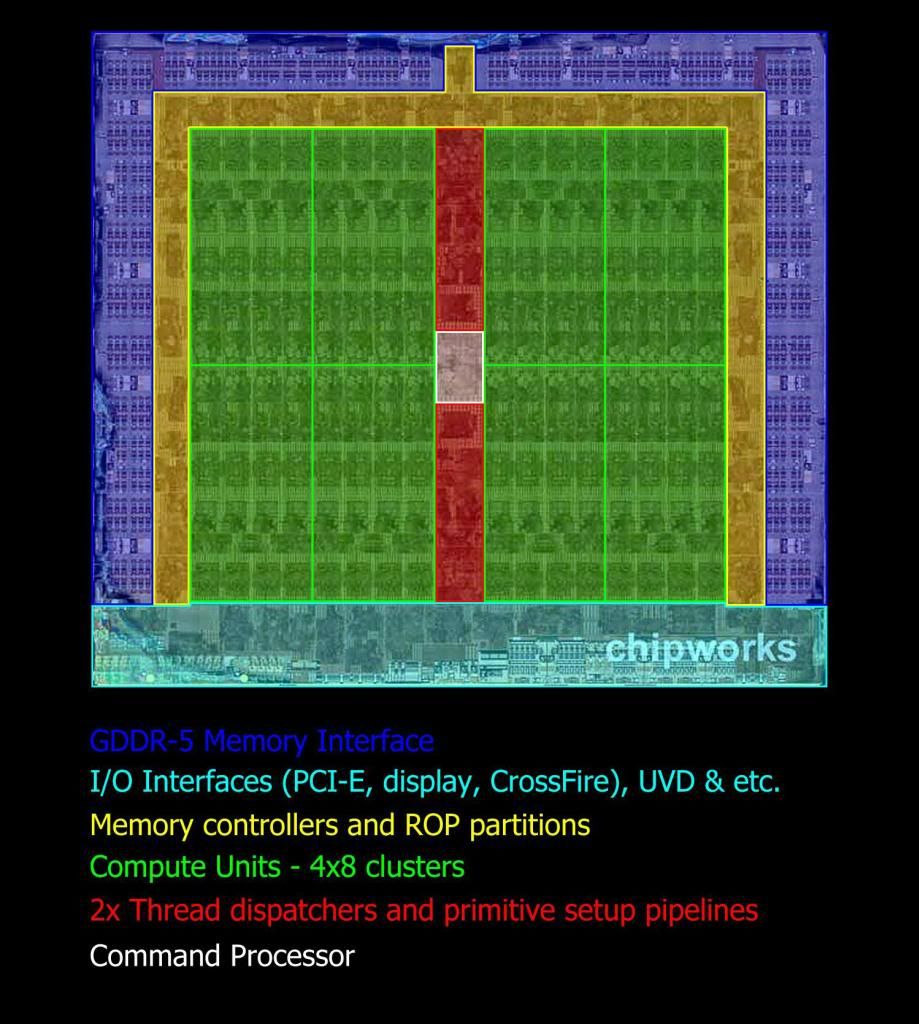
That's assuming that what we think are the texture units are actually texture units! What if the texture units are broken up, though? Let's say that the texture units are broken up a bit differently. You may have two blocks handling texture decompression (these would contain the L1 cache) and another two for the actual texture sampling and filtering. Q1 and Q2 may be the former, and T1 and T2 may be the latter. Their relative positions would be a bit odd, but very few positions seem to make sense on Latte.

On the other doubles, we could also have the ROPs divided into two. W1 and W2 might perform Z/stencil and U1 and U2 blend. That'd account for most of the double units, bar the small S1 and S2 blocks.

That is certainly an interesting proposition. I'll have to give it some thought. My gut feeling is that things are probably not that alien. Several blocks (V included) do seem to have direct counterparts in Llano. It's possible that things just look so strange to us because the design is different than the usual "ring" layout found in RV770 and Tahiti. Maybe spatial proximity isn't that important for some components either, so it was more a matter of, "How do we get all these blocks to fit on the die?"
 
How far are you guys in cracking this thing? Do you have a good idea of what it is now?
Yup, it's a complete alien encrypted thing compared to the best case scenario of what people expected which was looking at it and saying "oh, it's a R740 with some changes" or something along those lines, a clear heritage, intact. It's also way more custom than the original worst case scenario, at least mine.

Seems to be really well designed and thought out, it's clearly designed to make the most out of less so it wasn't lazy on any account; the bad news is that since it's not a by the book licensed thing with some changes on top everything sprouts doubts as whether it stayed the same (and just looks different!) or is really all that different. We also have a discrete GFlop ballpark for it now.

But it kept all these pages interesting.
 

z0m3le

Banned
So was the whole 9spu blocks debunked long ago? M certainly looks like it belongs in the N group to my relatively untrained eye, but has there been any serious posts about this idea?
 

Mildudon

Member
hey are such a technical company and they seem to be very open to answering technical question. Why don't people ask for their thoughts on the matters of the hardware functions? I'm sure they will give us some input. They seem like the most credible devs currently on the console.

I have asked them about the the tesselation unit in the wii u on twitter and havn't gotten a reply. Plus theres the NDA.
 

krizzx

Junior Member
I have asked them about the the tesselation unit in the wii u on twitter and havn't gotten a reply. Plus theres the NDA.

Have you tried emailing them? Perahps if you simply asked about functionality or something else. The NDS will likely stop them from giving anything direct, but I'm sure they can talk about things they have personally implemented like the Toki Tori dev with the memory freeing ability.
 
So was the whole 9spu blocks debunked long ago? M certainly looks like it belongs in the N group to my relatively untrained eye, but has there been any serious posts about this idea?

I don't know what it is, but it doesn't look like an SPU. Maybe it's a Global Data Share. Despite Thraktor's points, I still think there might be one on the chip. Otherwise, that 32 MB eDRAM would get pretty bogged down with all it's expected to do. Plus, eDRAM may not have a low enough latency to function as a GDS. Since we're talking a relatively low number of SPUs, perhaps Nintendo just decided to scratch the local data shares and add a fatter GDS. Ditto with L1 texture cache. If the on-chip bus is quick enough, Nintendo might have seen the additional phases as redundant in their already complex hierarchy. But I've got to do some more reading on the subject before I develop a more formed opinion on the matter.
 

Thraktor

Member
That is certainly an interesting proposition. I'll have to give it some thought. My gut feeling is that things are probably not that alien. Several blocks (V included) do seem to have direct counterparts in Llano. It's possible that things just look so strange to us because the design is different than the usual "ring" layout found in RV770 and Tahiti. Maybe spatial proximity isn't that important for some components either, so it was more a matter of, "How do we get all these blocks to fit on the die?"

I think we have to keep in mind that the die is almost certainly laid out by computer. The standard R700 dies we've been looking at have a large amount of by-hand organisation involved (principally the long SIMD arrays with texture units at the end), so the layout looks more "normal". By contrast, with a fully computer-laid die, the layout can look a lot more confusing, and even individual components can be distorted by the need to fit them in odd positions (eg N4).

So was the whole 9spu blocks debunked long ago? M certainly looks like it belongs in the N group to my relatively untrained eye, but has there been any serious posts about this idea?

M is an interesting one. Its location and size would point to a shader bundle, but the unusual SRAM configuration would seem to be a point against that.

Edit: I've added a small section to the OP with links to other VLIW5 die photos for comparison. I've only got RV770 and Llano at the moment, so any additions would be appreciated.
 
I think we have to keep in mind that the die is almost certainly laid out by computer. The standard R700 dies we've been looking at have a large amount of by-hand organisation involved (principally the long SIMD arrays with texture units at the end), so the layout looks more "normal". By contrast, with a fully computer-laid die, the layout can look a lot more confusing, and even individual components can be distorted by the need to fit them in odd positions (eg N4).


M is an interesting one. Its location and size would point to a shader bundle, but the unusual SRAM configuration would seem to be a point against that.

Edit: I've added a small section to the OP with links to other VLIW5 die photos for comparison. I've only got RV770 and Llano at the moment, so any additions would be appreciated.

Excellent! And yeah, those two dies are all I'm really working with at the moment. I've found die shots of Tahiti and Trinity as well, but as you know, they are probably not much help being a different architecture.

Formulating another crackpot theory at the moment. Let's see where this train of thought takes me...

Oh, and good point re: hand layout vs computer layout. I wasn't aware of such things.
 
I've been thinking alot about the double blocks on the processor. Looking at typical Radeon setups, and in particular Cyprus, might I suggest the following:

-2x Render Back Ends
-2x DDR3 dual channel memory controllers
-2x Color cache
-2x Z/Stencil Cache
-2x Rasterizer

This matches the amount of block pairs we have. There are other blocks which represent good candidates for the following: North Bridge, Command Processor, Geometry Assembly Processor, Vertex Assembly Processor (w/ tesselator), Ultrathreaded Dispatch Processor, Instruction Cache, Constant Cache, Vertex Cache, Global Data Share, and L2 Texture Cache (Block V for that last one - I'm thinking you were right, Thraktor!).

We've already identified (w/ some help, of course), the Pixel Shaders, TMUs, and South Bridge/DSP/ARM core. Oddly enough, no blocks seem to jump out as obvious Local Data Shares or L1 Texture Caches. In all designs from R700 onward, they are tightly grouped w/ the SIMD cores/TMUs.

If all of these blocks are present, which I suspect they are, there are few left over for any fixed function units. That's just as well, I say. I'd rather have the few extra pixel shaders and R700 generation ROPs! :p

Some of the bold seems a little much for what we're looking at. The Juniper line didn't double up on some of those and it clearly has more ALUs/SIMDs than what we're seeing.
 
Some of the bold seems a little much for what we're looking at. The Juniper line didn't double up on some of those and it clearly has more ALUs/SIMDs than what we're seeing.

Yeah, I'm starting to think that Thraktor is right and that the Z/Stencil and Color caches are inside the ROP blocks, although there would still be one of each cache for each render back end. 2 memory controllers might be necessary if we're talking 4 channels, no? The only other somewhat questionable item is the double rasterizer, but I'm thinking this might come in handy for rendering two discreet images simultaneously. Cayman doubled up its rasterizers without going the whole nine yards and doubling the whole Setup Engine, as the HD6000 series did in its higher end chips.

Edit: I wish somebody could step in and point out a ROP block on one or both of those reference chip images. All analyses I've come across just lump them together with memory controllers and L2 without discerning which is which.

Yeah I was focusing on the Z/Stencil and rasterizer. My feeling though is there wouldn't be a second rasterizer for the controller output. Juniper is Eyefinity-capable and only has one. Could be a part of why the controller impacts overall performance depending on what's displayed.

And which analyses have you come across?
 

ASIS

Member
We certainly have a better idea than before. I don't know if it will ever be "cracked" per say. If anything, it's bred some interesting discussion.

Yup, it's a complete alien encrypted thing compared to the best case scenario of what people expected which was looking at it and saying "oh, it's a R740 with some changes" or something along those lines, a clear heritage, intact. It's also way more custom than the original worst case scenario, at least mine.

Seems to be really well designed and thought out, it's clearly designed to make the most out of less so it wasn't lazy on any account; the bad news is that since it's not a by the book licensed thing with some changes on top everything sprouts doubts as whether it stayed the same (and just looks different!) or is really all that different. We also have a discrete GFlop ballpark for it now.

But it kept all these pages interesting.

Well that is excellent news. I truly commend you guys for your work.

But could you guys use english to describe the current expectations of the GPU, along with a best case and a worst case scenario?

No, I don't want this to start debates or comparisons to other consoles. I'm just interested and, well, the conversations here sound like you guys are speaking in swahili :p
 

Thraktor

Member
Well that is excellent news. I truly commend you guys for your work.

But could you guys use english to describe the current expectations of the GPU, along with a best case and a worst case scenario?

No, I don't want this to start debates or comparisons to other consoles. I'm just interested and, well, the conversations here sound like you guys are speaking in swahili :p

To put it in as simple terms as possible, I think the best Wii U games will look noticeably better than the best PS360 games, but not "Holy shit!" better. That is, if you had the best looking PS360 game and the best looking Wii U game next to each other, you'd say "The Wii U game definitely looks better", but you would't say "Holy shit, the Wii U game looks better!"
 

krizzx

Junior Member
To put it in as simple terms as possible, I think the best Wii U games will look noticeably better than the best PS360 games, but not "Holy shit!" better. That is, if you had the best looking PS360 game and the best looking Wii U game next to each other, you'd say "The Wii U game definitely looks better", but you would't say "Holy shit, the Wii U game looks better!"

To each his own on that one. I've already found a few Wii U games taht I would say look comparatively that much better.
 

tipoo

Banned
To each his own on that one. I've already found a few Wii U games taht I would say look comparatively that much better.

What on the U looks better than The Last of Us or Halo 4? I won't make the mistake of judging it by its launch games, but nothing I've seen has given me a "holy shit" moment that I thought the PS360 would never be capable of.
 

Thraktor

Member
To each his own on that one. I've already found a few Wii U games taht I would say look comparatively that much better.

Well, yeah, it's all subjective, really. I'm just saying that, while we should definitely see better-looking games, it won't be anything like a full generational leap.

On the artistic side, though, I'm sure EAD, Retro and Monolith should be able to do some really nice things.
 
To put it in as simple terms as possible, I think the best Wii U games will look noticeably better than the best PS360 games, but not "Holy shit!" better. That is, if you had the best looking PS360 game and the best looking Wii U game next to each other, you'd say "The Wii U game definitely looks better", but you would't say "Holy shit, the Wii U game looks better!"

Ah, this is essentially what I wanted to know. I never expected it to give us a full generational leap, but to hear that it will have room to grow from high end PS360 games is reassuring.
 
What on the U looks better than The Last of Us or Halo 4? I won't make the mistake of judging it by its launch games, but nothing I've seen has given me a "holy shit" moment that I thought the PS360 would never be capable of.

Someone's going to mention something, you're going to say you don't think it looks better, there's going to be back and forth and then it'll get lost in the scuffle of posts here
 

ASIS

Member
To put it in as simple terms as possible, I think the best Wii U games will look noticeably better than the best PS360 games, but not "Holy shit!" better. That is, if you had the best looking PS360 game and the best looking Wii U game next to each other, you'd say "The Wii U game definitely looks better", but you would't say "Holy shit, the Wii U game looks better!"

Oh well that's good to hear, thanks.
 
What on the U looks better than The Last of Us or Halo 4? I won't make the mistake of judging it by its launch games, but nothing I've seen has given me a "holy shit" moment that I thought the PS360 would never be capable of.
I wouldn't say that there is a single game on the WiiU that is above the PS360 level overall, but for example, I said "holy shit" at ZombiU's lighting (that surpasses everything I've seen on PS360 thanks to it's radiosity effect) or some nice effects from some of the attractions of Nintendo Land.

I think that Pikmin 3 will be the first game on sale that will make me say "holy shit" globally speaking, with maybe some minor flaws here and there, and of course in the future I expect to say "holy shit" (compared to PS360 levels, of course) in the sense that the game is completely superior in the bast majority of measurable things.
 
Someone's going to mention something, you're going to say you don't think it looks better, there's going to be back and forth and then it'll get lost in the scuffle of posts here

That's pretty much what's going to be 5 years from now when comparing the best looking games from 360/ps3 to wii u.
 
I wouldn't say that there is a single game on the WiiU that is above the PS360 level overall, but for example, I said "holy shit" at ZombiU's lighting (that surpasses everything I've seen on PS360 thanks to it's radiosity effect) or some nice effects from some of the attractions of Nintendo Land.
Yet, no one regards ZombiU graphics as great, high budget, next gen or "impressing".

We've come to a point where it's really subjective, up to art direction, doing something outlandish or just down to attention to detail and/or to scale (scale always impresses), really.

But the Wii U has more overhead and should be quite more efficient at doing some things current gen can't really think of with it's more modern feature set. Should be an interesting ride.


Halo 4 and The Last of Us are games that aren't gonna be humiliated by any next gen console too, I mean they're essentially very polished pieces of software with good artistic directions, and more than having power that's something that takes time to do these days; it's basically down to that, at worst Wii U will have to resort to the same pre-baked tricks and the like, but it's capable of pretty good graphics in the right hands, by any measure.
 
What's interesting about zombiU is the lightning technique used on the gamepad is different then the one on the main screen, and it's definitely a lot more impressive.


Does anyone know if this architecture is setup uniquely to handle rendering two frames at once?
 
Oh boy, I've got a doozy of a theory cooking up here, gentlemen! I need to research a bit more, but it seems to make sense of alot of what we're seeing.

Yeah I was focusing on the Z/Stencil and rasterizer. My feeling though is there wouldn't be a second rasterizer for the controller output. Juniper is Eyefinity-capable and only has one. Could be a part of why the controller impacts overall performance depending on what's displayed.

And which analyses have you come across?

Yeah, I'm edging away from the dual rasterizer hypothesis myself now. Check out this diagram by fellix on Beyond3D of Tahiti:

tahitidiagram.jpg


Check out the dual Thread Dispatchers on either end of the Command Processor. Look familiar? Similarly, there is one type of unit that DirectX 11 capable cards got rid of. Let's see if anyone figures out where I'm going with this...
 

Thraktor

Member
Missed this:

I don't know what it is, but it doesn't look like an SPU. Maybe it's a Global Data Share. Despite Thraktor's points, I still think there might be one on the chip. Otherwise, that 32 MB eDRAM would get pretty bogged down with all it's expected to do. Plus, eDRAM may not have a low enough latency to function as a GDS. Since we're talking a relatively low number of SPUs, perhaps Nintendo just decided to scratch the local data shares and add a fatter GDS. Ditto with L1 texture cache. If the on-chip bus is quick enough, Nintendo might have seen the additional phases as redundant in their already complex hierarchy. But I've got to do some more reading on the subject before I develop a more formed opinion on the matter.

I think something like an L1 texture cache is fairly essential. You need a cache (even a very small one) with that extremely low latency to operate efficiently.

The GDS, on the other hand, doesn't even need to have that low latency, it's only there to prevent the SIMD arrays having to go the whole way to (G)DDR and back to communicate with each other. The Nvidia GTX 400 series apparently had a 400-800 cycle latency to GDDR, so the handful of cycles it takes to get to the eDRAM back is no issue whatsoever in comparison.

Oh boy, I've got a doozy of a theory cooking up here, gentlemen! I need to research a bit more, but it seems to make sense of alot of what we're seeing.

I look forward to it :)
 
Oh boy, I've got a doozy of a theory cooking up here, gentlemen! I need to research a bit more, but it seems to make sense of alot of what we're seeing.

Now this is what I like to hear, I love hearing all of the possibilities for architecture. I had maybe one or two versions of what I thought the GPU would look like before we saw the die pictures.

Now that we've seen them all bets are off, and too hear all of the different speculation, as well as reasoning for the various architectures makes it feel as though were going through same conversations Nintendo went through when designing the MCM. Haha this has turned into a gaf reverse engineering project.
 
Alright, I may as well get to it.

I was looking at Latte's supposed TMUs and there's something off about them. Not adjacent to L1 cache like every other design we've seen. Seemingly mixed in with the front end of the GPU pipeline rather than the back end. It's all too much...

Actually, Thraktor, I can thank you for this one. You put the idea in my head that what we think are the TMUs might not necessarily be them in actuality. Compared to other TMU designs, there seems to be a distinct lack of SRAM in Latte's J blocks. The TMUs in Llano for instance aren't necessarily packed, but they have more than that.

Now, refer to the RV770 die photo linked to in the OP. Look at the bottom center. There is the block lined with SRAM on the perimeter similar to the (smaller) but similarly designed blocks on Tahiti which fellix has labelled the Thread Dispatch Units (see my previous post on this page). On RV770, that "fenced in" block is surrounded by 4 smaller blocks with just a tiny bit of SRAM - much like our J blocks on Latte.

The units I spoke of that are absent in Direct X 11 hardware are the Interpolation Units. Interpolation is done in the shaders these days. This is why we don't find them on Llano. But there happen to be 32 in the RV770 - a nice even multiple of 4.

So I'm proposing that the J blocks are not TMUs. They are Interpolation Units. A more logical place for the TMUs would be perhaps T1 and T2. It is possible that like the SPUs, they have doubled up the amount for each block. In fact, the S blocks could be L1 cache. If I'm eyeballing it correctly, it looks like they have 16kb each - exactly in line with what we would expect. Also, this puts the TMUs in close proximity to the V block, which would be our L2 cache in this hypothesis. It should be noted, in Llano, that V block is adjacent to the TMUs.

Alright, tear it to pieces. :p
 

IdeaMan

My source is my ass!
Its not such an off comparison. The hardware within Hollywood allowed effects to be produced at much lower resource costs than the same effect on the other consoles. It would be nice if they kept that component for at least auxiliary purposes in the Wii U's GPU.


One thing I would like to know is why people just don't ask the good devs for help? They seem to base all assumptions for the power of various Nintendo hardware on the worst ports and devs who have little to no experience with the hardware like the Metro Last Light dev. The more experienced devs like Shin'en, the Toki Tori dev and the Trine 2: DC dev seem to go completely ignored when they talk about the Wii U's technical capabilities. Its like journalists and even some professionals prefer the negative news and lean heavily towards the most negative possibilities.

http://www.notenoughshaders.com/2012/11/03/shinen-mega-interview-harnessing-the-wii-u-power/
For Nano Assault Neo we already used a few tricks that are not possible on the current console cycle.

If Shin'en were not the best at using the Wii's GPU, they were definitely in the top three. Just look at the work they did with Jett Rocket. http://jettrocket.wordpress.com/

They are such a technical company and they seem to be very open to answering technical question. Why don't people ask for their thoughts on the matters of the hardware functions? I'm sure they will give us some input. They seem like the most credible devs currently on the console.

I've conducted this interview, and believe me, it was quite hard to find the good questions and right approach to retrieve from them a few technical info :p "NDA R STRONG WITH THESE ONES" :p
 

krizzx

Junior Member
I've conducted this interview, and believe me, it was quite hard to find the good questions and right approach to retrieve from them a few technical info :p "NDA R STRONG WITH THESE ONES" :p

Ah, well then scratch that idea. Have you ever spoken with the devs of Trine 2 and Toki Tori?
 

IdeaMan

My source is my ass!
Ah, well then scratch that idea. Have you ever spoken with the devs of Trine 2 and Toki Tori?

I've submitted the die picture to several sources, waiting for news.

But the speculatanalysis of techies here is quite impressive and interesting :)
 
I've submitted the die picture to several sources, waiting for news.

But the speculatanalysis of techies here is quite impressive and interesting :)

We appreciate your efforts, IM! :)

Looking forward to having my theory on the last page ripped apart.

Also, blocks O and R seem quite strange to me. They are very large and have quite a bit of logic compared to SRAM. Perhaps they are Hollywood? Marcan seems to think the whole of it is basically on there, and those two blocks might represent a decent size estimate...

Edit: Reading through his tweets, it sounds like he now thinks there isn't any Hollyood logic on there. Who knows? For now, I nominate O and R to be candidates for "fixed function magic!" lol
 
I've submitted the die picture to several sources, waiting for news.

But the speculatanalysis of techies here is quite impressive and interesting :)

Do you think or have your sources told you that the GPU definitely has "secret sauce" or "Nintendo Magic" fused to the hardware (Fixed Functions)?

lol, this thread.....so much speculation you gotta love it.
 
Marcan seems to think the whole of it is basically on there, and those two blocks might represent a decent size estimate...

Edit: Reading through his tweets, it sounds like he now thinks there isn't any Hollyood logic on there. Who knows? For now, I nominate O and R to be candidates for "fixed function magic!" lol
They said he was trying to register here just yesterday and is now up for mod approval.

Looking forward to that.
 
They said he was trying to register here just yesterday and is now up for mod approval.

Looking forward to that.

Indeed, although it seems that he doesn't really care much about the things we care about. I think he already has the answers he wants, but maybe if we're completely off base, he'll pity us and share a bit more. haha
 
So between:

BG, Thraktor, Fourth Storm, Idea Man and Marcan we should finally figure this whole thing out?

I'm still trying to figure out why the Wii U GPU functions are under NDA.........What purpose does this serve to Nintendo even after the release of the console?
 
LOL. You made a funny Trev.

Alright, I may as well get to it.

I was looking at Latte's supposed TMUs and there's something off about them. Not adjacent to L1 cache like every other design we've seen. Seemingly mixed in with the front end of the GPU pipeline rather than the back end. It's all too much...

Actually, Thraktor, I can thank you for this one. You put the idea in my head that what we think are the TMUs might not necessarily be them in actuality. Compared to other TMU designs, there seems to be a distinct lack of SRAM in Latte's J blocks. The TMUs in Llano for instance aren't necessarily packed, but they have more than that.

Now, refer to the RV770 die photo linked to in the OP. Look at the bottom center. There is the block lined with SRAM on the perimeter similar to the (smaller) but similarly designed blocks on Tahiti which fellix has labelled the Thread Dispatch Units (see my previous post on this page). On RV770, that "fenced in" block is surrounded by 4 smaller blocks with just a tiny bit of SRAM - much like our J blocks on Latte.

The units I spoke of that are absent in Direct X 11 hardware are the Interpolation Units. Interpolation is done in the shaders these days. This is why we don't find them on Llano. But there happen to be 32 in the RV770 - a nice even multiple of 4.

So I'm proposing that the J blocks are not TMUs. They are Interpolation Units. A more logical place for the TMUs would be perhaps T1 and T2. It is possible that like the SPUs, they have doubled up the amount for each block. In fact, the S blocks could be L1 cache. If I'm eyeballing it correctly, it looks like they have 16kb each - exactly in line with what we would expect. Also, this puts the TMUs in close proximity to the V block, which would be our L2 cache in this hypothesis. It should be noted, in Llano, that V block is adjacent to the TMUs.

Alright, tear it to pieces. :p

From that viewpoint I'd guess I is the same that block the interpolators surround in the RV770 die shot.

Also, blocks O and R seem quite strange to me. They are very large and have quite a bit of logic compared to SRAM. Perhaps they are Hollywood? Marcan seems to think the whole of it is basically on there, and those two blocks might represent a decent size estimate...

Edit: Reading through his tweets, it sounds like he now thinks there isn't any Hollyood logic on there. Who knows? For now, I nominate O and R to be candidates for "fixed function magic!" lol

To me Shiota's comment was rather clear about not including Hollywood in the design.
 

tipoo

Banned
I'm still trying to figure out why the Wii U GPU functions are under NDA.........What purpose does this serve to Nintendo even after the release of the console?

Because Nintendo doesn't want people to fixate on the specs obviously. They don't know what kind of geeks we are though :p
 
From that viewpoint I'd guess I is the same that block the interpolators surround in the RV770 die shot.

Yes, "I" would be the Thread Dispatch Unit. It's obviously smaller on Latte. Perhaps because AMD shrunk the design themselves in more recent iterations (while not shrinking the interpolators, as they've been nixed) or perhaps it's just smaller because it has to deal with less threads.
 
Indeed, although it seems that he doesn't really care much about the things we care about. I think he already has the answers he wants, but maybe if we're completely off base, he'll pity us and share a bit more. haha
Perhaps, but he already had everything he needed sans-core die shot and has been looking at it nonetheless; I mean he keeps answering questions about his gut feeling regarding this.

Of course, hacking and gaining access to the full hardware is his focus, GPU actual features being secondary in that effort (and probably not his area of expertise seeing he strayed away from marking even the ALU's), but he's clearly interested nonetheless (he is trying to reverse engineer it after all). And he seems to like tech talk too.

I doubt he'll devote much time to theories and staying around, but still; would perhaps add something to the discussion and it's so much better than having twitter feeds with word limits.

Someone should ping a mod regarding this.
I'm still trying to figure out why the Wii U GPU functions are under NDA.........What purpose does this serve to Nintendo even after the release of the console?
They're NDA freaks and they don't want specs and general specifics lying around.

Pretty sure it also has to do with the competition; say they had "free vsync" via a custom built scanline renderer; chances are, they don't want Microsoft or Sony investing on implementing those same features hence they'll omit it since it should be transparent (although I'm not so sure that's at place). Some specifics, breakthroughs or shortcuts and their reason for being so might still be under wraps; at least until their competitors finish their spec, it's Nintendo I dunno but they should be as secretive regarding internal tech as they are when it comes to keep games and hardware close to their chest. But of course, Iwata also said the policy now was full disclosure and they should go for it, fact is; either their documentation and perhaps SDK is incomplete (might not be fully ready yet) or they might be holding out something.

Either awy at this point I wouldn't be surprised if even AMD/ATi isn't 100% sure of what's in the die seeing some changes and layout weren't implemented by them.
 
I'm still trying to figure out why the Wii U GPU functions are under NDA.........What purpose does this serve to Nintendo even after the release of the console?

When the Wii was first announced, we waited quite some time for the specs to come out as well. It was 'released' but a bunch of developers who worked on it and dev/hacking groups who managed to crack the Wii less than a month in.
 

Thraktor

Member
Alright, I may as well get to it.

I was looking at Latte's supposed TMUs and there's something off about them. Not adjacent to L1 cache like every other design we've seen. Seemingly mixed in with the front end of the GPU pipeline rather than the back end. It's all too much...

Actually, Thraktor, I can thank you for this one. You put the idea in my head that what we think are the TMUs might not necessarily be them in actuality. Compared to other TMU designs, there seems to be a distinct lack of SRAM in Latte's J blocks. The TMUs in Llano for instance aren't necessarily packed, but they have more than that.

Now, refer to the RV770 die photo linked to in the OP. Look at the bottom center. There is the block lined with SRAM on the perimeter similar to the (smaller) but similarly designed blocks on Tahiti which fellix has labelled the Thread Dispatch Units (see my previous post on this page). On RV770, that "fenced in" block is surrounded by 4 smaller blocks with just a tiny bit of SRAM - much like our J blocks on Latte.

The units I spoke of that are absent in Direct X 11 hardware are the Interpolation Units. Interpolation is done in the shaders these days. This is why we don't find them on Llano. But there happen to be 32 in the RV770 - a nice even multiple of 4.

So I'm proposing that the J blocks are not TMUs. They are Interpolation Units. A more logical place for the TMUs would be perhaps T1 and T2. It is possible that like the SPUs, they have doubled up the amount for each block. In fact, the S blocks could be L1 cache. If I'm eyeballing it correctly, it looks like they have 16kb each - exactly in line with what we would expect. Also, this puts the TMUs in close proximity to the V block, which would be our L2 cache in this hypothesis. It should be noted, in Llano, that V block is adjacent to the TMUs.

Alright, tear it to pieces. :p

Quite a reasonable theory, by the looks of it. The J's do look a lot like the small blocks next to the thread dispatch processor on the RV770, and I could be the thread dispatch unit itself. The only problem I have is the scale. On the RV770 the smaller blocks are about a quarter the size of the thread dispatch unit, but on Latte J1 itself is almost as big as I (bigger if we're only counting logic), and assuming interpolators would have a (roughly) linear relationship to shaders, there'd also be a mismatch there (with much fewer shaders, but the same number of interpolators as RV770).

There's another thing we have to consider for any theory about the J's is that J1 is significantly bigger than the others. I did a quick calculation, and J2 (excluding SRAM) comes to 66,126 pixels, whereas J1 (again ex. SRAM) comes to 142,955. This means the actual logic on J1 is just over twice as big as on J1-J3. If they are texture units, then my theory is that J1 does double-duty as Wii mode's texture unit, but if they're something like interpolators then we're going to need a reason why one's so much bigger than all the others.

On the subject of doubled-up texture units, I agree with you, although I don't think the S units would be caches (too much logic). They might be texture decompression units with L1 cache included, though, which I'd previously posited the Q blocks might be.

We appreciate your efforts, IM! :)

Looking forward to having my theory on the last page ripped apart.

Also, blocks O and R seem quite strange to me. They are very large and have quite a bit of logic compared to SRAM. Perhaps they are Hollywood? Marcan seems to think the whole of it is basically on there, and those two blocks might represent a decent size estimate...

Edit: Reading through his tweets, it sounds like he now thinks there isn't any Hollyood logic on there. Who knows? For now, I nominate O and R to be candidates for "fixed function magic!" lol

I'm quite puzzled about O and R myself, and I don't really know what GPU components would require a lot of logic with very little SRAM.

To me Shiota's comment was rather clear about not including Hollywood in the design.

I'm not so sure. What I read into it is that some of the Hollywood functions would be handled by Latte units (eg J1 in my scenario above), but that doesn't necessarily mean there isn't any Hollywood hardware in there. There may have been Hollywood functions where it was simpler to just include the block directly on Latte rather than try to shoe-horn it into a more modern unit. I'd expect maybe one or two Hollywood blocks somewhere on the die, but not much more than that.
 

nordique

Member
Welcome back bgassassin! :) (though I should be saying fancy seeing you here around this time, since I too took a hiatus...and still sorta desire it...but Gaf...it just keeps pulling you back in!)


and just also generally wanted to say you guys are doing an amazing analysis. I'm sure i'm one of many lurking, enjoying this greatly.

Great job to Thraktor, blu, Fourth Storm, Durante, wsippel, et al involved at analysing and critiquing this stuff so far.
 

Popstar

Member
There's another thing we have to consider for any theory about the J's is that J1 is significantly bigger than the others. I did a quick calculation, and J2 (excluding SRAM) comes to 66,126 pixels, whereas J1 (again ex. SRAM) comes to 142,955. This means the actual logic on J1 is just over twice as big as on J1-J3. If they are texture units, then my theory is that J1 does double-duty as Wii mode's texture unit, but if they're something like interpolators then we're going to need a reason why one's so much bigger than all the others.
J1 looks like it might actually be two elements to me. Split down the middle. But it's like reading tea leaves.
 
Quite a reasonable theory, by the looks of it. The J's do look a lot like the small blocks next to the thread dispatch processor on the RV770, and I could be the thread dispatch unit itself. The only problem I have is the scale. On the RV770 the smaller blocks are about a quarter the size of the thread dispatch unit, but on Latte J1 itself is almost as big as I (bigger if we're only counting logic), and assuming interpolators would have a (roughly) linear relationship to shaders, there'd also be a mismatch there (with much fewer shaders, but the same number of interpolators as RV770).

There's another thing we have to consider for any theory about the J's is that J1 is significantly bigger than the others. I did a quick calculation, and J2 (excluding SRAM) comes to 66,126 pixels, whereas J1 (again ex. SRAM) comes to 142,955. This means the actual logic on J1 is just over twice as big as on J1-J3. If they are texture units, then my theory is that J1 does double-duty as Wii mode's texture unit, but if they're something like interpolators then we're going to need a reason why one's so much bigger than all the others.

On the subject of doubled-up texture units, I agree with you, although I don't think the S units would be caches (too much logic). They might be texture decompression units with L1 cache included, though, which I'd previously posited the Q blocks might be.

Thanks for the feedback. Yeah, the ratio of the proposed Interpolators to SPUs is a good point to raise. I simply don't know enough to say how these things usually scale. I'd say we shouldn't assume it's a linear relationship with this little to go on, though. Even if they don't usually scale the way we see here, who's to say Nintendo didn't have their own reasons for including all of them? It's something worth looking into, definitely.

In regards to the size of J1, that's another curiosity. I can only guess, but perhaps it has something to do with how the data is passed from the dispatch unit to the interpolators. If we assume that's what they are, in the old RV770 design, all the interpolators border the dispatch unit. Here, only one does. The intricacies of die layout may have prevented it. So perhaps that one has some extra logic on board to make up for this. I'm in over my head already with this stuff, though. So I'll stop there. :p

I don't think the S blocks have too much logic to be texture caches. Take a look at the texture caches on Llano and RV770. They need logic to keep doing what they do automatically.

J1 looks like it might actually be two elements to me. Split down the middle. But it's like reading tea leaves.

Haha, this is some serious voodoo shit going on here. I actually thought that myself, though, about J1. It still has the same amount of SRAM as the others, though.
 

wsippel

Banned
Yeah, the J units are weird. Actually, almost every block that isn't a shader cluster is weird.

I think a good question would be: If someone wanted to improve GPUs, not bound by PC conventions and not general purpose, what would he do? And by "improve", I don't necessarily mean "make it faster".
 
Quite a reasonable theory, by the looks of it. The J's do look a lot like the small blocks next to the thread dispatch processor on the RV770, and I could be the thread dispatch unit itself. The only problem I have is the scale. On the RV770 the smaller blocks are about a quarter the size of the thread dispatch unit, but on Latte J1 itself is almost as big as I (bigger if we're only counting logic), and assuming interpolators would have a (roughly) linear relationship to shaders, there'd also be a mismatch there (with much fewer shaders, but the same number of interpolators as RV770).

There's another thing we have to consider for any theory about the J's is that J1 is significantly bigger than the others. I did a quick calculation, and J2 (excluding SRAM) comes to 66,126 pixels, whereas J1 (again ex. SRAM) comes to 142,955. This means the actual logic on J1 is just over twice as big as on J1-J3. If they are texture units, then my theory is that J1 does double-duty as Wii mode's texture unit, but if they're something like interpolators then we're going to need a reason why one's so much bigger than all the others.

This old B3D post I came across while looking for more info on interpolators suggests both the RV670 (320 ALUs) and the RV770 have the same amount.

http://forum.beyond3d.com/showpost.php?p=1193433

Messing about with some silly shaders in GPUSA it appears that both RV670 and RV770 have 32 interpolators:

That said my against point would come from this article in 2009:

http://techreport.com/review/17618/amd-radeon-hd-5870-graphics-processor/5

AMD CTO Eric Demers pointed out in his introduction to the Cypress architecture that the RV770's interpolation hardware had become a performance-limiting step in some texture filtering tests, and using the SIMDs for interpolation should bypass that bottleneck.

Considering the time you'd think/hope Nintendo knew this early on. It would seem better to implement AMD's method to address the issue than keep the problem or take a different approach to address it.

I'm not so sure. What I read into it is that some of the Hollywood functions would be handled by Latte units (eg J1 in my scenario above), but that doesn't necessarily mean there isn't any Hollywood hardware in there. There may have been Hollywood functions where it was simpler to just include the block directly on Latte rather than try to shoe-horn it into a more modern unit. I'd expect maybe one or two Hollywood blocks somewhere on the die, but not much more than that.

The way I see it is that parts of Latte and Espresso could already emulate parts of Broadway and Hollywood and when they thought Wii circuits needed to be added, the engineers from IBM and AMD were able to tweak certain parts of Wii U instead keeping it smaller.
 
The way I see it is that parts of Latte and Espresso could already emulate parts of Broadway and Hollywood and when they thought Wii circuits needed to be added, the engineers from IBM and AMD were able to tweak certain parts of Wii U instead keeping it smaller.

I'm not sure why people would interpret it otherwise. Almost seems like that part was mentioned to explicitly clear confusion and yet people are choosing to interpret it in different ways
 
Status
Not open for further replies.
Top Bottom