• Hey, guest user. Hope you're enjoying NeoGAF! Have you considered registering for an account? Come join us and add your take to the daily discourse.

WiiU "Latte" GPU Die Photo - GPU Feature Set And Power Analysis

Status
Not open for further replies.
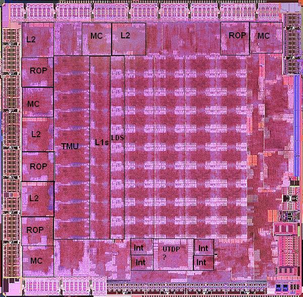
I'm not really worthy of this thread (knowledge + language), but I've been wondering if this AMD patent application titled "DYNAMIC CONTROL OF SIMDs" (filed 07/12/2011) has anything to do with the Wii U GPU (or CPU - I'm clueless).

It could be totally generic and already being widely used on a bunch of -commercial- GPUs, so be nice :p (searched thread/gaf)

It tickled my interest because it's aimed at reducing power consumption and achieving "optimal usage of the graphics processing unit" and because of the time-frame it was filed (July 2011).

I understand that it's something that doesn't have to be exclusive to the WiiU - I'm just asking of what are the chances it's being used here.

Summary:
Embodiments of the present invention enable power saving in a graphics processing unit by dynamically activating and deactivating individual SIMDs in a shader complex that comprises multiple SIMDs. On-the-fly dynamic disabling and enabling of individual SIMDs provides flexibility in achieving a required performance and power level for a given processing application. In this way, optimal usage of the graphics processing unit can be achieved.

...

Embodiments of the present invention can be used in any computing system (e.g., a conventional computer (desktop, notebook, etc.) system, computing device, entertainment system, media system, game systems, communication device, personal digital assistant), or any system using one or more processors.

/resumes lurking mode
 
Ok, thanks.

The problem I have again here is with the size of those R700 interpolation blocks vs Latte's "J" blocks.

If you scale Latte and the R700 die to the correct sizes relative to each other Latte's J blocks are bigger than the interpolation units on R700. Now I know die shrinks are never linear, especially when it comes to logic, but we can both agree that if those are both the same units the Latte block should certainly be significantly smaller and certainly not bigger. It gets even more disproportionate if you compare the memory on each block. The memory in Latte's J block is over twice the size of the memory inside R700's interpolation blocks.

R700_I_vs_Latte_J.jpg


The S blocks actually fit the kind of size we should be seeing from those interpolation units on a 40nm process (obviously I can't say for sure, just roughly fit as in they're around half the size), and they also look very similar to what you highlighted on the R700 die. However there's only two of those and the memory config doesn't match up in size.

Comparing Latte's J blocks to R700's TMU's shows that they're roughly the right size considering the process difference (about half the size of R700's TMU's) but the memory amount doesn't seem to match either (hard to tell accurately because of how low detail the R700 shot is but they certainly don't seem to match). Still I suppose that's less of a problem than neither size or memory matching, as maybe they altered the memory configuration?

The size of the shader blocks in R700 match up with what I already compared between Latte and Brazos. The R700 shader blocks are slightly bigger than Latte blocks and very slightly smaller than Brazos blocks. But of course on a 55nm process 20 SP blocks in R700 should be only slightly smaller than the 40 SP blocks we see in Brazos on a 40nm process.

Hmmm. Well, I suppose this is as good a time as any to bring up a few points that were shared with me by somebody who has some knowledge of these matters. I think he prefers to remain anonymous and not get dragged into this madness. :p

Disclaimer: I'm not trying to use this to dismiss the size differences. Thanks for that comparison. Just think these points might aid our discussion/slightly lessen confusion.

Anyway, when it comes to fabrication processes and making comparisons between Latte and other chips, a few things should be kept in mind:

Process nodes do not necessarily describe the size you can expect out of individual components. Particularly, between two fab houses (in this case, Renesas and TSMC), electrical characteristics and transistor densities can vary greatly, making comparisons between the two for our purposes not very helpful.

AMD optimizes their GPU designs for TSMC's fabs, so the densities that come out are bound to be excellent. It is unknown how similar the Renesas fab tech is to the bulk Si/gate-last process used by TSMC.

Sizes can also differ over time even on the same process node/fab house. For example, the PS2 chipset was shrunk significantly even on the same process. Basically, experience matters, and Latte being a first run for this design at this fab, things might not have shrunk down so optimally.

There are also different transistor design targets which will affect die size, such as high-performance and low power. We don't really know what Nintendo/Renesas were aiming for with Latte.

Even with all that being true, my informant found the near equivalent size of Latte's blocks and the 55nm RV770 blocks to be somewhat of a head-scratcher. It would be great if we could get absolute confirmation on the process node used (I'm working on that, but no guarantee of success). Of course, there are also the unknowns of how BC is implemented, but it's probably some additional logic spread throughout the individual blocks which allow them to function as their Wii analogues (not the actual Wii parts, but logic to essentially run the emulation layer). Who knows how much that adds up to? And there could be other modifications, of course, as well. I wouldn't expect anything quite magic, and any speculation would just be a shot in the dark, but it bears noting.

Hopefully that info proves enlightening to some. I know it did for me.

Edit: Bgassasin, thanks for that breakdown. I don't know if I have really much to address right now. The only thing is that Block V, imo, must be either GDS or L2 cache. I lean towards GDS because RV770 had individual L2s (64 kB each, which I am assuming were halved for Latte's leaner setup) and the U blocks kind of look like em. I may get around to doing an annotation of RV770, but as you can probably tell, art is not my forte and it would be largely guesswork anyway besides what I've already pointed out. The L2 should be fairly obvious on that die though - the blocks around the outside perimeter, adjacent to the GDDR3 interface that have that World Trade Center-looking stack of SRAM (yeah, that's my best description haha). So anyway, I'm guessing that GDS is one of the other things that Nintendo beefed up to be more in line with Recent AMD cards - making it 64kB rather than the paltry 16kB of the HD4000 series. Don't think that's too out there, given their comments on being "memory centric" and a "GPGPU."
 

Earendil

Member
Oh boy, here we go! :p

The block diagram is useful in some situations, it seems, but not in others. For example, it makes sense for most of the setup engine blocks to lie in close proximity. It makes sense for LDS to be by the shaders and L1 to be adjacent to the TMUs. It can be deceptive in other instances, however, agreed. The shader export/sequencer on Brazos is a good example. Then again, Brazos as a whole is a very unique design and the overall layout seems to represent a significant departure from the flagship GPUs of that generation.


Yes, Brazos has alot of consolidation going on. In fact, this is one reason why I don't think it's that great of a candidate for a Latte comparison in the finer details. They both share the common Radeon base, but not much more. Brazos was obviously designed around achieving maximum density and interfacing with the on-die CPU cores.

I don't see Latte as having that same amount of consolidation going on. In the past, I've listed geometry setup and vertex setup as different blocks. Looking at the number of discreet blocks on Latte, I'm thinking that is still the case. My point was more to show that the tesselator and HiZ don't seem to be getting their own blocks. Thus, the magic number of "5" can be discarded and there is no reason ponder a dual setup engine. As I implied in that large post a few pages back, I'm not really concerned about identifying every single block in Latte at this point - it's seemingly impossible without some very creative guesswork. haha

As for TAVC, I still have every reason to believe that's texture related. The "TD" block on Brazos is quite small for 8 TMUs, and looking at how they split up the ROPs, I think they probably did the same thing with the texture units. "TD" could actually just be "texture decompressor" or texture filter units while "TAVC" could be the texture address processors. Either way, I don't think that's what is going on with Latte. T1 and T2 just look so much like the RV770 TMU blocks, that there would need to be some serious evidence to convince me otherwise at this point. The Brazos die shot has been helpful in our discussion, but I still think R700 is where we should be looking when trying to decode the Latte layout.


As I said in that previous post, I don't think Latte has the same split of color buffer and depth buffer that we see in Brazos. I think that the design is closer to RV770 and both of the W blocks contain 4 of each. None of the blocks in question on Brazos are exact matches for W. The ROPs on Brazos do support my argument that we should be looking for them close to the DDR3 interface, however. With the possibility that devs may not have (or have had) access to the eDRAM, that makes more sense. Even if they are using the eDRAM as framebuffer, I don't think being a couple blocks away will increase latency to the point that things become a problem. I don't know how latency-sensitive that sort of thing is anyway, considering that most framebuffers are off chip and even Wii had to output the front buffer to the off-chip 24MB 1t-SRAM before it went out to the display.


Yes, I've speculated in the past that Nintendo beefed up the constant cache in their initiative to improve compute on Latte. The more I look, the more I see the resemblance between SQ on Brazos and D on Latte. Good eyes, bg! To me, it doesn't really matter if block D is the UTDP or just holds the caches which interact with that processor. Having it all in one block may be another instance of consolidation in Brazos or it may always be like that. Either way, it's still close to the placement I propose for the setup engine and interpolators.


Is that true? I did a quick search and I did find one article that mentions the lack of UTDP, but are we sure that's really the case or is it just an assumption they drew from the vague block diagram? Those very long yellow blocks on the sides of the Tahiti Block diagram may be meant to represent the UTDP, as they are also close to the two caches they need access to. But yeah, if I isn't the UTDP and it's just everything in D, that's not a deal breaker for me.


I've gone back and forth many times on the Q blocks. Right now, I'm back to them being a couple of DDR3 controllers. In both Brazos and Llano, we see the NB adjacent to the memory phy -just like the display controller is by the display phy and so on with PCIe, etc. Assuming this, I'd still have B as a NB, but only for the CPU to access MEM1. Those two small doublet blocks on Llano still seem to resemble Q somewhat, but my search for their functionality hasn't turned up much.

I thought my awful paint job would bring more clarity, but it seems to have caused confusion! :( As I alluded to earlier, I am in the camp that Latte contains 2 RV770 TMU blocks and 2 RV770 style L1 caches (and probably two RV770 style L2 caches as well in the U blocks). In the area I circled in Brazos, you can see, within that consolidated block, two separate identical groups, which I identify as 2x L1s. As I pointed out a few pages back, in RV770, it appears that both the L1 cache and LDS are placed between the TMUs and shader cores, so I don't think direct contact between the texture units and ALUs is a necessity.

Your thoughts are welcome, as always! Let me know if you think of any of those other points!

I generally consider myself to be a reasonably intelligent person, but this is making my head hurt. There's a reason I stick to software these days.
 

wsippel

Banned
Even with all that being true, my informant found the near equivalent size of Latte's blocks and the 55nm RV770 blocks to be somewhat of a head-scratcher. It would be great if we could get absolute confirmation on the process node used (I'm working on that, but no guarantee of success). Of course, there are also the unknowns of how BC is implemented, but it's probably some additional logic spread throughout the individual blocks which allow them to function as their Wii analogues (not the actual Wii parts, but logic to essentially run the emulation layer). Who knows how much that adds up to? And there could be other modifications, of course, as well. I wouldn't expect anything quite magic, and any speculation would just be a shot in the dark, but it bears noting.

Hopefully that info proves enlightening to some. I know it did for me.
Renesas UX7LSeD 55nm eDRAM has a cell size of 0.12 square micron. 32MB would therefore require 32212254.72 square micron, or 32.2mm² - just for the cells. MEM1 is 41mm².
 
Edit: Bgassasin, thanks for that breakdown. I don't know if I have really much to address right now. The only thing is that Block V, imo, must be either GDS or L2 cache. I lean towards GDS because RV770 had individual L2s (64 MB each, which I am assuming were halved for Latte's leaner setup) and the U blocks kind of look like em. I may get around to doing an annotation of RV770, but as you can probably tell, art is not my forte and it would be largely guesswork anyway besides what I've already pointed out. The L2 should be fairly obvious on that die though - the blocks around the outside perimeter, adjacent to the GDDR3 interface that have that World Trade Center-looking stack of SRAM (yeah, that's my best description haha). So anyway, I'm guessing that GDS is one of the other things that Nintendo beefed up to be more in line with Recent AMD cards - making it 64MB rather than the paltry 16MB of the HD4000 series. Don't think that's too out there, given their comments on being "memory centric" and a "GPGPU."

Oh, I'm asking you to annotate only what you've pointed out not guess what you don't know. That's what I essentially did. I annotated the blocks I thought were similar in Brazos and Llano. I'm hoping to get a better picture of why you are making the RV770 comparisons by asking you to do the same. I'm not an art person either and just used Gimp for labeling.
 

z0m3le

Banned
Hopefully that info proves enlightening to some. I know it did for me.

Didn't TSMC fab this chip? also it being 55nm would at this point be impossible considering the eDRAM memory correct? If it's 55nm things do make more sense, however that is something I've moved away from thinking as it would mean more dense than TSMC's run and again that memory should be way bigger at 55nm or am I wrong?

There are times when people simply make reality fit their ideas and not coming up with new ideas to conform to reality, that is why I ask. I think honestly Latte's unknowns will remain that and that some trying to figure it out will only beat their heads against the wall eventually.

From a performance standpoint nothing we come up with will actually change how Wii U is seen, the reality is that the console is marginally more capable than last gen consoles, Wii U benefits greatly from having a more modern set up and much more RAM available to developers. If Xenos really did only see 60% efficiency and was discovered that only 217ALUs were usable, I think 160 even VLIW5 ALUs would be efficient enough to beat it out.

A quick napkin math explanation of this is Xenos using 217ALUs clocked at 500MHz with a 60% efficiency is roughly firing 130ALUs at a time. Wii U's GPU being VLIW5, normally in a PC would reach ~68% efficiency or ~3.4ALUs out of every 5. in a console though, 4 ALUs would be very easy to get "firing" in every instruction, there is still a fifth and would activate some of the time. lets say 4.4ALUs out of every 5 fire, or 88% efficiency with Wii U in it's current state. (lack of experience and early tools) Now lets say it has 160ALUs at 88% efficiency Wii U would have 140ALUs "firing" at any one time, and thanks to the 10% overclock the base performance of these ALUs would be the same as 154 xenos ALUs in comparison with xenos, this doesn't take into account modern feature sets and SM4.1 which is vastly superior in performance overall to SM3. These claims also have to take into account XB1 is suppose to reach 66% more efficiency over Xenos, which puts it above 99% efficiency so 88% for Wii U definitely shouldn't be far fetched and considering Nintendo's customization of this chip whatever that may be, it could see shaving at that number for a while.

TL;DR: It doesn't take much to beat Xenos it seems.

So whether it is 160ALUs and a ridiculously mysterious bulking of the GPU or a 320ALUs being a bit more dense than previous 40nm produces from 2010, I think it doesn't matter much, the golf between the visuals is tiny and even XB1 is going to show it's lack of performance at launch. For that matter PS4 is still a fairly minimal jump for what gamers were expecting, but given time all 3 platforms will prove to bury last gen consoles by a noticeable amount.

Prepare for some silly but maybe valid comparisons:

I'm tempted to even say that 360 vs Wii U will end up looking more like Genesis vs SNES but there really isn't much I can compare XB1 and PS4 to in that instance, maybe the best I can do is compare the genesis add-ons to them. Sega-CD for XB1 and Sega 32X for PS4 (I believe the 32X had more performance on paper.) You'd see in things like Doom on 32X vs SNES where XB1 and Wii U might align, such as better IQ, textures and such from the 32X (ignore the superior audio in the SNES as that shouldn't be present in XB1 vs Wii U comparison and if it were, it would likely go the other way as XB1 has optical audio)
 

Donnie

Member
Fourth Storm

Yep different fabs will produce different results and different blocks will shrink differently. I agree that makes a lot of sense, especially with most blocks having varying ratio's of logic to memory.

But as you say what you shouldn't see is similar blocks being as big on a 40nm process as they are on a 55nm process. Especially in the case of the R700 interpolaters vs Latte's "J" blocks. They should basically be identical units, so to have the 40nm one bigger is absolutely unheard of and to me means they aren't what you think they are.

The difference in size of shader units is less clear. Could be extra custom logic of various kinds, as well as partly down to slightly different fab processes (TSMC vs Renesas, though as far as we know Latte could be produced at TSMC). But to me the obvious answer is still more SP's, I don't see any reason why it should be ruled out or even thought of as less than likely (it could even be 32 per block).

I think eventually we might find out how many shader units we have in there, but it might be years from now unfortunately, until then all we're going to have is theories.
 
I never suggested 55nm! Indeed, by my measurements of a single yellow block of MEM1 (no spaces), it would be too small for Renesas' 55nm eDRAM and more in line with the 40nm figures they posted back in 2009.

Wish the software I got from CW still worked. Seems like a file got corrupted and it went kaput. And I don't know if the POS desktop I'm working on could even run GIMP, bg. haha. I'm holding out for haswell to get a new laptop.
 

Earendil

Member
Oh, I'm asking you to annotate only what you've pointed out not guess what you don't know. That's what I essentially did. I annotated the blocks I thought were similar in Brazos and Llano. I'm hoping to get a better picture of why you are making the RV770 comparisons by asking you to do the same. I'm not an art person either and just used Gimp for labeling.

I've been using Photoshop for 18 years, so I could certainly help with any needed "art".
 

Schnozberry

Member
The difference in size of shader units is less clear. Could be extra custom logic of various kinds, as well as partly down to slightly different fab processes (TSMC vs Renesas, though as far as we know Latte could be produced at TSMC). But to me the obvious answer is still more SP's, I don't see any reason why it should be ruled out or even thought of as less than likely (it could even be 32 per block).

The heat spreader on the MCM doesn't list TSMC anywhere, but Renesas is listed prominently. I suppose it doesn't rule out a TSMC fab, but I lean Renesas.
 
Fourth Storm

Yep different fabs will produce different results and different blocks will shrink differently. I agree that makes a lot of sense, especially with most blocks having varying ratio's of logic to memory.

But as you say what you shouldn't see is similar blocks being as big on a 40nm process as they are on a 55nm process. Especially in the case of the R700 interpolaters vs Latte's "J" blocks. They should basically be identical units, so to have the 40nm one bigger is absolutely unheard of and to me means they aren't what you think they are.

The difference in size of shader units is less clear. Could be extra custom logic of various kinds, as well as partly down to slightly different fab processes (TSMC vs Renesas, though as far as we know Latte could be produced at TSMC). But to me the obvious answer is still more SP's, I don't see any reason why it should be ruled out or even thought of as less than likely (it could even be 32 per block).

I think eventually we might find out how many shader units we have in there, but it might be years from now unfortunately, until then all we're going to have is theories.

There may be something else going on in those blocks, as well. After all, J1 is larger than the other blocks, which aren't uniform in size, either. They may even be augmented somewhat since their limited functionality in R700 was a source of complaints (and why in R800 series interpolation was moved to the ALUs). So yeah, there are definitely some unanswered questions. I'm quite confident that they are not TMUs at this point, however. The SRAM configuration similarities between Latte's S1 and S2 and the L1 texture caches in both Llano and Brazos are conclusive, in my eyes.
 

Donnie

Member
The heat spreader on the MCM doesn't list TSMC anywhere, but Renesas is listed prominently. I suppose it doesn't rule out a TSMC fab, but I lean Renesas.

I think Renesas definitely have the contract, but with them outsourcing a lot of chips to TSMC as you say it can't be ruled out. Chipworks themselves thought it was probably TSMC (despite them no doubt seeing the Renesas listing on the heat spreader).
 

Donnie

Member
There may be something else going on in those blocks, as well. After all, J1 is larger than the other blocks, which aren't uniform in size, either. They may even be augmented somewhat since their limited functionality in R700 was a source of complaints (and why in R800 series interpolation was moved to the ALUs). So yeah, there are definitely some unanswered questions. I'm quite confident that they are not TMUs at this point, however. The SRAM configuration similarities between Latte's S1 and S2 and the L1 texture caches in both Llano and Brazos are conclusive, in my eyes.

It would definitely help if you could do some form of annotation of the die shots just showing what you believe each block to be (not every block just what you've identified).

Are you saying you believe S1 and S2 to be Latte's TMU's or am I misunderstanding you here?

EDIT: Oh actually you believe T1 and T2 are the TMU's yes?
 

Schnozberry

Member
There may be something else going on in those blocks, as well. After all, J1 is larger than the other blocks, which aren't uniform in size, either. They may even be augmented somewhat since their limited functionality in R700 was a source of complaints (and why in R800 series interpolation was moved to the ALUs). So yeah, there are definitely some unanswered questions. I'm quite confident that they are not TMUs at this point, however. The SRAM configuration similarities between Latte's S1 and S2 and the L1 texture caches in both Llano and Brazos are conclusive, in my eyes.

Would changes need to be made to the interpolators at a hardware level for complete code compatibility with the Wii? It could explain some of the size difference. I know Marcan mentioned the 8-bit CPU doing the code translation, but I am skeptical of that being the only change that was necessitated.
 

ozfunghi

Member
I never suggested 55nm! Indeed, by my measurements of a single yellow block of MEM1 (no spaces), it would be too small for Renesas' 55nm eDRAM and more in line with the 40nm figures they posted back in 2009.

Wish the software I got from CW still worked. Seems like a file got corrupted and it went kaput. And I don't know if the POS desktop I'm working on could even run GIMP, bg. haha. I'm holding out for haswell to get a new laptop.

Paintdotnet is easier to comprehend (if you know photoshop) and i think it also runs faster than gimp, but it's not the better program.
 

z0m3le

Banned
Would changes need to be made to the interpolators at a hardware level for complete code compatibility with the Wii? It could explain some of the size difference. I know Marcan mentioned the 8-bit CPU doing the code translation, but I am skeptical of that being the only change that was necessitated.

the 8bit CPU is only for video compatibility, it doesn't have to do with TEV logic, however Flipper is only 26 million transistors so even including the entire gamecube GPU wouldn't result in the difference in size seen (that is the transistor count minus the t1-sram btw) TEV logic plays a small role in the bulk we see.
 

Schnozberry

Member
the 8bit CPU is only for video compatibility, it doesn't have to do with TEV logic, however Flipper is only 26 million transistors so even including the entire gamecube GPU wouldn't result in the difference in size seen (that is the transistor count minus the t1-sram btw) TEV logic plays a small role in the bulk we see.

I thought marcan implied that the 8-bit CPU was translating TEV instructions into something the programmable shaders could understand. I probably just misunderstood what he said.
 

Donnie

Member
joesiv

If its not too much trouble could you try to do the same thing with the RV770, Brazos and Llano die shots some time?
 
Alright, here's what I see as going on around the perimeter of RV770. It's a bit hard to tell where some blocks end and other begin, but this should more or less give some idea of where I'm coming from. I've labeled what must be the L2 cache blocks. The other blocks I've outlined are either memory controllers or ROPs. No way for me to say which is which.
rv770annotated.jpg


Hmm, actually if I were to take a guess, I would say that the highlighted block all the way to the top right (with it's small portion of brighter SRAM), would be a memory controller. Descriptions of the layout have memory controllers paired w/ the L2 and ROPs. Obviously the actual die is a bit messier, but if we are to go on that, then the block to the left of that separated block of L2 on top should be a memory controller. I don't think the ROPs and L2s interact with each other, so there would be no need for them to be in close proximity.

Edit: I've revised the annotation to reflect these thoughts.

Edit: Nice work, joesiv!

I think Renesas definitely have the contract, but with them outsourcing a lot of chips to TSMC as you say it can't be ruled out. Chipworks themselves thought it was probably TSMC (despite them no doubt seeing the Renesas listing on the heat spreader).

The TSMC/Renesas connection was for 28nm only, I believe. Either way, I am pretty sure that the 40nm TSMC remark was just an offhand guess by Jim. He said as much to me in a later email. I've heard another source state that it is, indeed, Renesas doing the manufacturing, which would match the heat spreader and comments from the Iwata Asks on the Wii U hardware.

EDIT: Oh actually you believe T1 and T2 are the TMU's yes?

Yes, and S1 and S2 would be the L1 texture caches aligned with the TMUs in all Radeon designs from the past 5 years or so.

Would changes need to be made to the interpolators at a hardware level for complete code compatibility with the Wii? It could explain some of the size difference. I know Marcan mentioned the 8-bit CPU doing the code translation, but I am skeptical of that being the only change that was necessitated.

I don't know how interpolation was handled on Gamecube and Wii. blu might be able to answer that one. And as stated, the 8-bit CPU is for the video signal. There's other logic somewhere on the GPU die handling TEV code translation. I've speculated that it's in the shader units themselves, going on that quote by Shiota in the OP (also originally from that Iwata Asks).
 

joesiv

Member
If its not too much trouble could you try to do the same thing with the RV770, Brazos and Llano die shots some time?
I don't know if it's as needed for the Llano die, as it's details weren't as mushy as the WiiU's GPU shot. However, I did some tweaks anyways, and did some rough blocking (sorry I have no experience doing that, hopefully I didn't block it totally wrong ha ha):

Blocked: LlanoDie_blocked.jpg
Unblocked: LlanoDie.jpg

small version:
LlanoDie_blocked-small.jpg


Does anyone have better versions of the R770, or a Brazos die shot? The R770 shot in the OP is pretty small, probably wouldn't be worth tweaking, and I didn't see a Brazos shot. Bigger the better, uncompressed ideal!
 
Looks good, joesiv, except each C block is actually two blocks. The top portion is the L1 cache, all-important to our discussion.

I believe "H" and "G" are identical.

Q is the display controller and analagous to Latte's F block. Both appear near the display phy and have 32 of those small SRAM banks.
 
Does the top section of C include or not the row of darker parts? I can cut it above or below that row of dark bits.

I would cut it above that row of dark bits. That's how I see it at least, but I don't want to be accused of changing blocks to fit my theory. :p

Also, I don't know if "D" is two blocks or not. Looks like it could be...
 

joesiv

Member
I would cut it above that row of dark bits. That's how I see it at least, but I don't want to be accused of changing blocks to fit my theory. :p

Also, I don't know if "D" is two blocks or not. Looks like it could be...

I've split up the C blocks, I'll go with your theory, it could either way IMO :D

As for D, I'll leave it as is for now, I'll update the files if there are any further changes that need to be made.

Oh, I've also tweaked the shading to be easier on the eyes ;)
 

Mr_B_Fett

Member
Disclaimer: I'm not trying to use this to dismiss the size differences. Thanks for that comparison. Just think these points might aid our discussion/slightly lessen confusion.

Anyway, when it comes to fabrication processes and making comparisons between Latte and other chips, a few things should be kept in mind:

Process nodes do not necessarily describe the size you can expect out of individual components. Particularly, between two fab houses (in this case, Renesas and TSMC), electrical characteristics and transistor densities can vary greatly, making comparisons between the two for our purposes not very helpful.
Absolutely, but Renesas have been busy divesting their fab plants over the past year or two as part of their "fab-lite" strategy so it's quite possible that TSMC are handling the manufacture.

AMD optimizes their GPU designs for TSMC's fabs, so the densities that come out are bound to be excellent. It is unknown how similar the Renesas fab tech is to the bulk Si/gate-last process used by TSMC.
Not really, AMD has historically been exclusive to (and will be again) Global Foundries which was spun-out of AMD. It's only the recent 28nm APUs that TSMC handle. Also TSMC only switched to gate-last at 28nm.

Sizes can also differ over time even on the same process node/fab house. For example, the PS2 chipset was shrunk significantly even on the same process. Basically, experience matters, and Latte being a first run for this design at this fab, things might not have shrunk down so optimally.
Yup, but this was a pretty long development cycle.

There are also different transistor design targets which will affect die size, such as high-performance and low power. We don't really know what Nintendo/Renesas were aiming for with Latte.

True, but I would say that by targeting a fixed and relatively low clock speed you are giving yourself the best chance of increasing density and optimising power usage whilst maintaining good yields.
 
Absolutely, but Renesas have been busy divesting their fab plants over the past year or two as part of their "fab-lite" strategy so it's quite possible that TSMC are handling the manufacture.


Not really, AMD has historically been exclusive to (and will be again) Global Foundries which was spun-out of AMD. It's only the recent 28nm APUs that TSMC handle. Also TSMC only switched to gate-last at 28nm.


Yup, but this was a pretty long development cycle.


True, but I would say that by targeting a fixed and relatively low clock speed you are giving yourself the best chance of increasing density and optimising power usage whilst maintaining good yields.

Thanks for the insight. TSMC and AMD go a bit further back, though, don't they? I was aware of GF only recently (was it last year or the year before?) becoming their own entity. However, Brazos is a 40nm TSMC design, I believe.
 

Mr_B_Fett

Member
Thanks for the insight. TSMC and AMD go a bit further back, though, don't they? I was aware of GF only recently (was it last year or the year before?) becoming their own entity. However, Brazos is a 40nm TSMC design, I believe.

Sorry, it would appear I was talking absolute rubbish. TSMC was ATI's fab partner and continued to do most of manufacture post AMD. GF was born out of The Foundry Company which was the spin-out of AMDs fab. I should know better than to post from memory. Yup looks like Brazos 2.0 was the first CPU/APU to be produced by TSMC for AMD and it was at 40nm.
 
People who are passionate about computer graphics have had fun speculating and nothing has been confirmed.

From the outside looking in (I know nothing about this) I'm wondering why even bother when we know it's underpowered. The Wii U is just slightly more powerful than the 360 and PS3. Why waste any significant time at all trying to analyze its GPU? It's like writing a thesis for your PhD on a Transformers film in the sense that you've wrote this incredible, detailed, well-researched paper for an incredibly crappy film.
 

krizzx

Junior Member
People who are passionate about computer graphics have had fun speculating and nothing has been confirmed.

I wouldn't say we have learned nothing. We have learned have learned a great deal, just little that is finite.

We were making pretty stead progress for a while, but it seems that all progress came to a halt when the 160 ALU hypothesis reared its head. Until that is resolved, it doesn't look like things will progress much further from there barring another leak or if a known dev with experience on the hardware divulges some information.

A few misconceptions have been cleared though.


We know that there are no discernible memory bottlenecks despite early proposals from B3D.
We know that its "not" a 4650 contrary to what Eurogamer stated with absolute unyielding certainty. Its a completely custom chip.
We know that it is capable of functional tessellation thanks to Shin'en.
"I" believe that it is capable of at least twice the polygon throughput. Also another reason why I am leaning towards the dual graphics engine hypothesis.

Besides that, we've opened up possibilities that weren't taken into consideration in the beginning. I'd say things are progressing.

From the outside looking in (I know nothing about this) I'm wondering why even bother when we know it's underpowered. The Wii U is just slightly more powerful than the 360 and PS3. Why waste any significant time at all trying to analyze its GPU? It's like writing a thesis for your PhD on a Transformers film in the sense that you've wrote this incredible, detailed, well-researched paper for an incredibly crappy film.

Huh? Underpowered in regards to what? How do you define underpowered and on the off chance that it is, what bearing does that have on wanting to know the functionality and capability of the chip? That sounds more like your own presumptions and you wanting analysis to stop for fear that it may be proven otherwise. You seem to misunderstand the reason why it is being analyzed to begin with. We aren't fanboys doing this for fanboyish reasons.

Please enlighten us as to how you know its underpowered. To date, the only aspect of the console that any devs have made a complaint about is the CPU. They all seem to be in agreement that the GPU and Memory is superior. /not underpowered.

http://gamersxtreme.org/2013/05/30/...is-much-more-powerful-than-most-people-think/
 
I want to be optimistic and say we actually know a lot by now - but we don't really understand it.

Same here. Btw, someone mentioned you dug up something on Latte having UVD. Is this true? If so, that block has gotta be somewhere and I have an idea that might hinge on it.
 
The Wii U is just slightly more powerful than the 360 and PS3. Why waste any significant time at all trying to analyze its GPU? It's like writing a thesis for your PhD on a Transformers film in the sense that you've wrote this incredible, detailed, well-researched paper for an incredibly crappy film.

Hahahaha.

That's, literally, the BEST summation of this thread on the last few pages.

Please brace for those who still feel there's some Nintendo-exclusive techniques that will make the Wii U incredibly overpowered
 

JordanN

Banned
Huh? Underpowered in regards to what? How do you define underpowered and on the off chance that it is, what bearing does that have on wanting to know the functionality and capability of the chip?
I think he means underpowered similar to how the Wii was back in 2006.

The sheer power difference between Wii U and PS4/XBO will make ports really hard or downright impossible for the majority of devs. This isn't debatable.
 

krizzx

Junior Member
I think he means underpowered the same way the Wii was back in 2006.

The sheer power difference between Wii U and PS4/XBO will make ports impossible to the majority of devs. This isn't debatable.

How will that make it impossible for ports when the Wii received ports from the 360/PS3 and the PS3/360, which are weaker than the Wii U, will still be receiving ports from the PS4 and XboxOne? What aspects of difference in hardware strength on this scale make porting "impossible"?

I'm not even going to get into this. I know its pointless.
 

tkscz

Member
From the outside looking in (I know nothing about this) I'm wondering why even bother when we know it's underpowered. The Wii U is just slightly more powerful than the 360 and PS3. Why waste any significant time at all trying to analyze its GPU? It's like writing a thesis for your PhD on a Transformers film in the sense that you've wrote this incredible, detailed, well-researched paper for an incredibly crappy film.

a.aaa-No-fun-allowed..jpg
 

JordanN

Banned
How will that make it impossible for ports when the Wii received ports from the 360/PS3 and the PS3/360, which are weaker than the Wii U, will still be receiving ports from the PS4 and XboxOne? What aspects of difference in hardware strength on this scale make porting "impossible"?

I'm not even going to go into this one. I know its pointless.
PS3/360 aren't going to be supported forever nor do I expect certain next gen games to run on them (GTA 6?).

As for aspects, how about the fact the PS4/XBO are 10x better, have huge pools of RAM and utilize DirectX 11 tech? Downporting from all of this may be too much for alot of developers (with little reason to care) and that's where they'll call it quits.
 

tipoo

Banned
I don't want to read 6000+ posts so can someone please summarize what is known?

"It seems to run on some form of electricity!"


If you're genuinely curious, we know the main memory bandwidth is 12.8GB/s, the eDRAM is 65-140 (thanks for the correction), the GPU is about 700 million transistors and the eDRAM on it was about 200 iirc, the shaders look weirdly fat and it's unknown whether it's 160 shaders with some sort of fattening (perhaps for compute, like the geforce 500 series had fatter less numerous shaders) or there are more shaders per cluster at 320. We know the eDRAM is 32MB. 8 ROPs is a high probability guess.

The rest of the thread padding has been lots of theorizing.
 
PS3/360 aren't going to be supported forever nor do I expect certain next gen games to run on them (GTA 6?).

As for aspects, how about the fact the PS4/XBO are 10x better, have huge pools of RAM and utilize DirectX 11 tech? Downporting from all of this may be too much for alot of developers and that's where they'll call it quits.

10x better at what? See, there's the point of the thread.
 
Status
Not open for further replies.
Top Bottom