• Hey, guest user. Hope you're enjoying NeoGAF! Have you considered registering for an account? Come join us and add your take to the daily discourse.

AMD Reports 2016 Second Quarter Results + Conference Call

R

Rösti

Unconfirmed Member
SUNNYVALE, CA -- (Marketwired) -- 07/21/16 -- AMD (NASDAQ: AMD) today announced revenue for the second quarter of 2016 of $1,027 million, operating loss of $8 million, and net income of $69 million, or $0.08 per diluted share. Non-GAAP (1) operating income was $3 million and non-GAAP (1) net loss was $40 million, or $0.05 per share.

Q2 2016 Results

  • Q2 2016, Q1 2016 and Q2 2015 were 13-week fiscal quarters.
  • Revenue of $1,027 million, up 23 percent sequentially and up 9 percent year-over-year primarily due to higher sales of semi-custom SoCs.
  • Gross margin of 31 percent, down 1 percentage point sequentially, due primarily to a higher mix of semi-custom SoC sales.
  • Operating expenses of $353 million, compared to $344 million for the prior quarter. Non-GAAP operating expenses of $342 million, compared to non-GAAP operating expenses of $332 million in Q1 2016, primarily due to increased marketing investments.
  • Operating loss of $8 million, compared to an operating loss of $68 million in Q1 2016. Non-GAAP(1) operating income of $3 million, compared to non-GAAP(1) operating loss of $55 million in Q1 2016, primarily due to higher sales.
  • Net income of $69 million, earnings per share of $0.08, and non-GAAP(1) net loss of $40 million, non-GAAP(1) loss per share of $0.05. This is compared to a net loss of $109 million, loss per share of $0.14 and non-GAAP(1) net loss of $96 million, non-GAAP(1) loss per share of $0.12 in Q1 2016. The GAAP sequential and year-over-year improvements were primarily due to a gain of $150 million related to the formation of our assembly, test, mark and pack (ATMP) joint venture (JV) with Nantong Fujitsu Microelectronics Co., Ltd. (NFME), partially offset by related taxes of $27 million. The non-GAAP sequential and year-over-year improvements were primarily due to higher sales and an IP licensing gain.
  • Cash and cash equivalents were $957 million at the end of the quarter, up $241 million from the end of the prior quarter, primarily due to net cash proceeds received from the ATMP JV transaction with NFME which closed in Q2 2016.
  • Total debt at the end of the quarter was $2.24 billion, flat from the prior quarter.
Financial Segment Summary
  • Computing and Graphics segment revenue of $435 million decreased 5 percent sequentially and increased 15 percent from Q2 2015. The sequential decrease was primarily due to decreased sales of client desktop processors and chipsets and the year-over-year increase was driven primarily by increased notebook processor and GPU sales.
  • Operating loss was $81 million, compared with an operating loss of $70 million in Q1 2016 and an operating loss of $147 million in Q2 2015. The sequential increase was primarily due to lower revenue. The year-over-year improvement was primarily due to higher revenue and lower operating expenses.
  • Client average selling price (ASP) increased sequentially driven by a higher desktop processor ASP and decreased year-over-year primarily due to lower notebook processor ASP.
  • GPU ASP remained flat sequentially and decreased year-over-year. The year-over-year decrease was primarily driven by lower desktop GPU ASP.
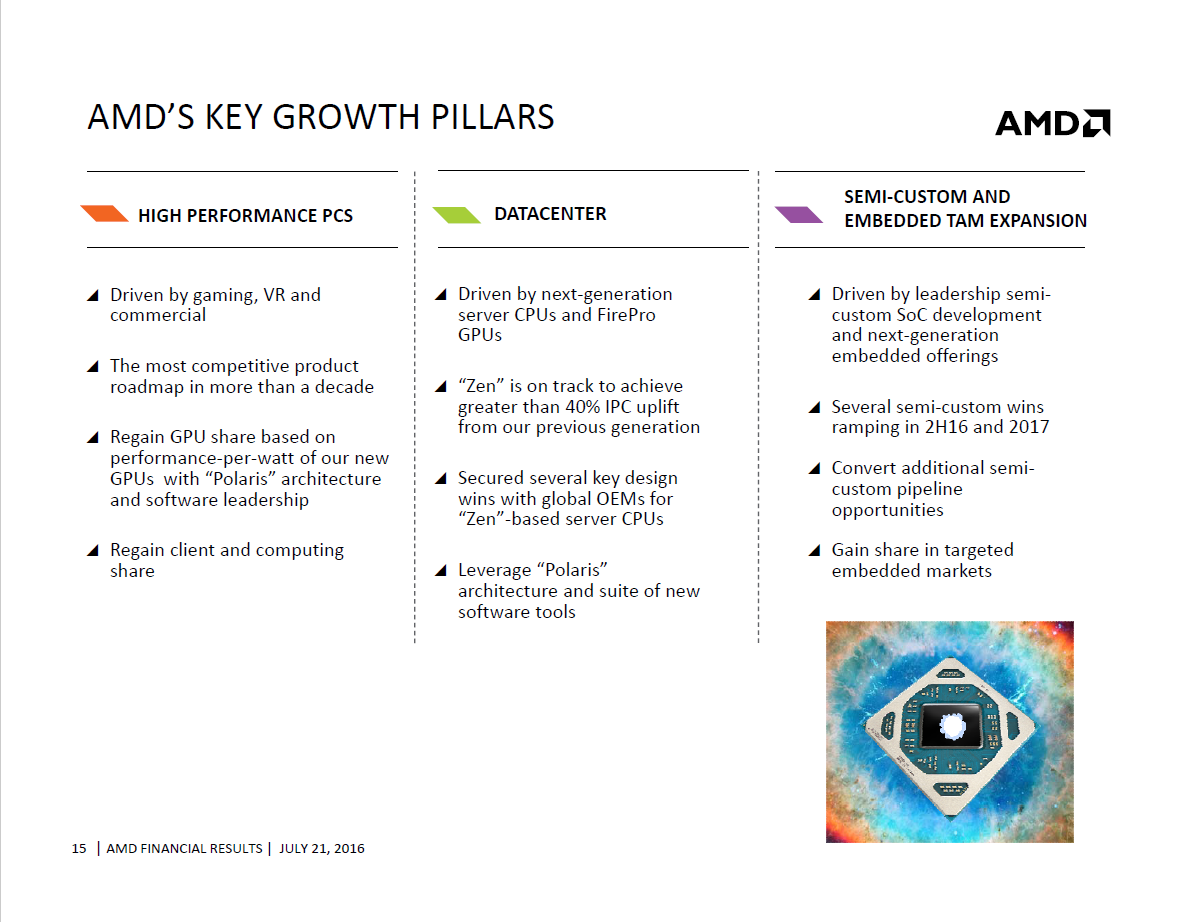
  • Enterprise, Embedded and Semi-Custom segment revenue of $592 million increased 59 percent sequentially and increased 5 percent year-over-year due to higher sales of semi-custom SoCs.
  • Operating income was $84 million compared with $16 million in Q1 2016 and $27 million in Q2 2015 primarily due to higher revenue from the sale of semi-custom SoC products and a $26 million IP licensing gain in Q2 2016 compared to $7 million in Q1 2016.
  • All Other category operating loss was $11 million compared with $14 million in Q1 2016 and $17 million in Q2 2015.
Source: http://ir.amd.com/phoenix.zhtml?c=74093&p=irol-newsArticle&ID=2187336

Conference call at 2 PM PST: http://ir.amd.com/phoenix.zhtml?c=74093&p=irol-eventDetails&EventId=5231046

AMD Teleconference
AMD will hold a conference call for the financial community at 2:00 p.m. PDT (5:00 p.m. EDT) today to discuss its second quarter financial results. AMD will provide a real-time audio broadcast of the teleconference on the Investor Relations page of its website at www.amd.com. The webcast will be available for 12 months after the conference call.
 
I love this GAAP stuff

We made $3 million from operations!

Fiddles with numbers [GAAP]

Ah ha not really! We lost $8 million.

Operating loss of $8 million, compared to an operating loss of $68 million in Q1 2016. Non-GAAP(1) operating income of $3 million, compared to non-GAAP(1) operating loss of $55 million in Q1 2016, primarily due to higher sales.

Anyway essentially they are breakeven and have enough cash on hand, hopefully Radeon 480 does well since it looks like the best value $200 card. I have nVidia GPU but competition is good.
 
I love this GAAP stuff

We made $3 million from operations!

Fiddles with numbers [GAAP]

Ah ha not really! We lost $8 million.


Anyway essentially they are breakeven and have enough cash on hand, hopefully Radeon 480 does well since it looks like the best value $200 card. I have nVidia GPU but competition is good.

I have a 1070, but I am absolutely hoping that the high end AMD cards are as impressive as the 480. NVIDIA needs a good kick in the ass right now.
 
R

Rösti

Unconfirmed Member
The presentation slides are up, they can be downloaded here: http://ir.amd.com/phoenix.zhtml?c=74093&p=irol-eventDetails&EventId=5231046

slide7tsmr.png


slide2misjs.png
 

SMattera

Member
I love this GAAP stuff

We made $3 million from operations!

Fiddles with numbers [GAAP]

Ah ha not really! We lost $8 million.

Actually, it's the other way around. Companies start with GAAP and then fiddle with the numbers to make them look better.
 

Duxxy3

Member
Hopefully the 480 and Zen are able to turn around AMD. Nvidia and Intel need somebody to keep them grounded.
 

THE:MILKMAN

Member
The second bullet point under 'broaden our technology reach' is interesting given it seems to me that that is exactly what AMD and Sony have done with the Neo APU.

Maybe it would be overstating the situation but I wonder if its true Sony have planned Neo all along (before PS4) then could they have had a hand in the design of Polaris?

Or is that crazy talk?
 

Sinistral

Member
But Polaris's performance-per-watt ended up not being too impressive compared against Nvidia's offerings, right? Unless AMD cards perform better in non-game use cases (which I've been wondering about, given their high FLOPS ratings but meh results).

True, but compared to their last generation of products it is a significant step forward. They'll sell them at extremely slim margins to remain competitive, as is always the case.
 
It'll be most interesting to see what their Q3 looks like. But what is really important will be their Zen line of processors their performance and TDP/Efficiency. When is their new CPU line slated?
 

IcyStorm

Member
But Polaris's performance-per-watt ended up not being too impressive compared against Nvidia's offerings, right? Unless AMD cards perform better in non-game use cases (which I've been wondering about, given their high FLOPS ratings but meh results).

They won't be close to catching Pascal for some time. But it is a substantial upgrade from AMD's previous generation of cards.
 

SRG01

Member
For more context, this stock has been on fire since their Q1 ER. AMD has literally been outperforming every stock in my portfolio despite buying *after* their Q1 report.

Also, it beat consensus earnings by three cents, which is huge.

They won't be close to catching Pascal for some time. But it is a substantial upgrade from AMD's previous generation of cards.

That's a deliberate strategy by AMD. Pascal's die size is huge compared to Polaris. Yields favor smaller dies so AMD will be able to push out more product for less money -- especially when it comes to wafer purchases.
 
D

Deleted member 465307

Unconfirmed Member
True, but compared to their last generation of products it is a significant step forward. They'll sell them at extremely slim margins to remain competitive, as is always the case.

That makes sense. And their roadmap suggests that performance-per-watt results will continue to show big improvements as they move to Vega and Navi. The 480's 4 GB model is a great value (and the 8 GB as well, to a lesser but still impressive degree), so I guess we'll find out in 3 months if that helped them out.
 
Have they announced projected operating income/loss for the next quarter?

It seems from reviews the Radeon 480 makes a lot of sense for a $200 budget GPU thats powerful enough for VR. As I recall from reviews, the 480 is the best value at $200 though you do get more performance with a 1060 though its $250+

So hopefully they can get a high yield on the new process and make a ton of cash with these 480's. It certainly opens up PC based VR for a much lower price point vs back in the 970+ days.

At least they basically broke even on an operating basis and have a lot of cash on hand (though over $2B in debt)
 

IcyStorm

Member
It'll be most interesting to see what their Q3 looks like. But what is really important will be their Zen line of processors their performance and TDP/Efficiency. When is their new CPU line slated?

Zen is still for Q1 2017... with rumors of a possible late Q4 2016 release.
 
But Polaris's performance-per-watt ended up not being too impressive compared against Nvidia's offerings, right? Unless AMD cards perform better in non-game use cases (which I've been wondering about, given their high FLOPS ratings but meh results).

RX480 performance per watt wasn't impressive, but if you believe AMD's statements, RX470 and RX480M are more efficient. Supposedly RX480 was simply pushed into less efficient territory to hit the required performance numbers. Also, if you look at Nvidia's numbers, GP106 is less efficient than GP104, which is similar to what has happened with earlier generations. The GP104 territory seems to be where the perf/W is best thanks to a more optimal mix of shaders/memory bus/etc.

amd-radeon-rx-470-rx-480m-performance-20160615.jpg
 

Renekton

Member
For more context, this stock has been on fire since their Q1 ER. AMD has literally been outperforming every stock in my portfolio despite buying *after* their Q1 report.
The run-up on AMD stock is about as dumb as the one for Nintendo after Pokemon GO.

AMD needs to get into the black consistently. Maybe get into more JVs with tech-starved China.
 
The second bullet point under 'broaden our technology reach' is interesting given it seems to me that that is exactly what AMD and Sony have done with the Neo APU.

Maybe it would be overstating the situation but I wonder if its true Sony have planned Neo all along (before PS4) then could they have had a hand in the design of Polaris?

Or is that crazy talk?
Not crazy at all. Cerny and friends have been working on GCN for a while now.
The three "major modifications" Sony did to the architecture to support this vision are as follows, in Cerny's words:

  • "First, we added another bus to the GPU that allows it to read directly from system memory or write directly to system memory, bypassing its own L1 and L2 caches. As a result, if the data that's being passed back and forth between CPU and GPU is small, you don't have issues with synchronization between them anymore. And by small, I just mean small in next-gen terms. We can pass almost 20 gigabytes a second down that bus. That's not very small in today’s terms -- it’s larger than the PCIe on most PCs!
  • "Next, to support the case where you want to use the GPU L2 cache simultaneously for both graphics processing and asynchronous compute, we have added a bit in the tags of the cache lines, we call it the 'volatile' bit. You can then selectively mark all accesses by compute as 'volatile,' and when it's time for compute to read from system memory, it can invalidate, selectively, the lines it uses in the L2. When it comes time to write back the results, it can write back selectively the lines that it uses. This innovation allows compute to use the GPU L2 cache and perform the required operations without significantly impacting the graphics operations going on at the same time -- in other words, it radically reduces the overhead of running compute and graphics together on the GPU."
  • Thirdly, said Cerny, "The original AMD GCN architecture allowed for one source of graphics commands, and two sources of compute commands. For PS4, we’ve worked with AMD to increase the limit to 64 sources of compute commands -- the idea is if you have some asynchronous compute you want to perform, you put commands in one of these 64 queues, and then there are multiple levels of arbitration in the hardware to determine what runs, how it runs, and when it runs, alongside the graphics that's in the system."
"The reason so many sources of compute work are needed is that it isn’t just game systems that will be using compute -- middleware will have a need for compute as well. And the middleware requests for work on the GPU will need to be properly blended with game requests, and then finally properly prioritized relative to the graphics on a moment-by-moment basis."

This concept grew out of the software Sony created, called SPURS, to help programmers juggle tasks on the CELL's SPUs -- but on the PS4, it's being accomplished in hardware.


The team, to put it mildly, had to think ahead. "The time frame when we were designing these features was 2009, 2010. And the timeframe in which people will use these features fully is 2015? 2017?" said Cerny.
(emphasis mine (not sure if "regular" GCN has the other stuff too))
http://www.gamasutra.com/view/feature/191007/inside_the_playstation_4_with_mark_.php
 

dr_rus

Member
There's a rather surprising amount of revenue coming from semi-custom business. It seems that AMD may actually get some solid income from all these console contracts they've managed to win in case they'll be able to maintain that revenue in the following quarters.

That's a deliberate strategy by AMD. Pascal's die size is huge compared to Polaris. Yields favor smaller dies so AMD will be able to push out more product for less money -- especially when it comes to wafer purchases.

Pascal's relative die sizes are smaller than that of Polaris even despite it being on a wee bit less dense production process.
 

Eradicate

Member
EDIT: From transcript found here: http://seekingalpha.com/article/3990485-advanced-micro-devices-amd-lisa-t-su-q2-2016-results-earnings-call-transcript?part=single (May have to sign up for a free account.)

Mark Lipacis - Jefferies LLC

Okay. Great. A follow-up, if I may. I was hoping that you could just help me with the accounting of the semi-custom design wins. If I remember properly, there was two that you expect in the back half of this year and then one, I thought it was the first half of next year. So Scorpio is one of those three? But that's next year. So that's the one for next year?

Lisa T. Su - President, CEO & Non-Independent Director

Yeah, let me help you out with the accounting. I know that we've had several different pieces of information on the semi-custom new design wins. So, what we've said is we'll have a total of three semi-custom new design wins that will account for about, let's call it $1.5 billion of revenue, approximately, over the next three to four years. We're starting the ramp of new business this coming quarter, this third quarter, and that will be one of the semi-custom design wins. Scorpio is also a design win, and that, as our customer has said, will be in 2017, and we'll give you more information about the third one as we have more visibility.

Mark Lipacis - Jefferies LLC

And do you have more design wins that you just haven't announced or mentioned timing of?

Lisa T. Su - President, CEO & Non-Independent Director

Well, we're trying to get out a little bit of the counting game, but I think, overall, we're pleased with the semi-custom pipeline. I think some of the questions that we've been asked are, do we believe we have design wins outside of game consoles, and the answer is yes. We have design wins outside of game consoles. I think we view the pipeline as good and it's a business model that works well with our high performance technology slant and our SoC capabilities.

For context for everyone!

Dumb question probably, but are they considering VR hardware as design wins?
 

ethomaz

Banned
Any shipment number for semi-custom console chips???

That's a deliberate strategy by AMD. Pascal's die size is huge compared to Polaris. Yields favor smaller dies so AMD will be able to push out more product for less money -- especially when it comes to wafer purchases.
Pascal is smaller than Polaris... I don't know where you read the opposite.
 

thefro

Member
Dumb question probably, but are they considering VR hardware as design wins?

VR hardware would only be a design win if it has an AMD semi-custom chip in it.

Most of the VR stuff I've seen is just a headset that connects to a PC, PS4, phone, etc (which actually powers the graphics).
 

LordOfChaos

Member
But Polaris's performance-per-watt ended up not being too impressive compared against Nvidia's offerings, right? Unless AMD cards perform better in non-game use cases (which I've been wondering about, given their high FLOPS ratings but meh results).

No, but it's also thought the high end Polaris parts will use TSMC, while the mid range 480 used the more inefficient GloFo process to fill out their wafer agreement (which is set to hamper them until 2024, sadly).

So all may not be lost on the efficiency front. I think Pascal will still be more efficient on the same process, but Polaris could close the gap significantly on a good process. AMD also likes to leave in more compute stuff than Nvidia, the 1070 and 1080 can trade blows with AMD cards there, but for each price class AMD has more compute, those two can brute force past AMD cards out right now. That'll matter more for async and GPGPU in games.

That's a deliberate strategy by AMD. Pascal's die size is huge compared to Polaris. Yields favor smaller dies so AMD will be able to push out more product for less money -- especially when it comes to wafer purchases.

RX480 is 232mm2, GTX 1060 was around 200mm2 iirc? So Pascal is actually smaller per unit performance. But like I said for equivalent price ranges AMD also leaves in more compute and DP, and then there's also that the 1060 no longer has SLI so may have saved a bit of die there, uses a narrower bus, etc.
 

THE:MILKMAN

Member
VR hardware would only be a design win if it has an AMD semi-custom chip in it.

Most of the VR stuff I've seen is just a headset that connects to a PC, PS4, phone, etc (which actually powers the graphics).

Could, for example, Nintendo's 'supplementary computing device' count as not a console?

serversurfer said:
Not crazy at all. Cerny and friends have been working on GCN for a while now.

To my mind it makes perfect sense but I'm just not sure if they really would cooperate as closely as I think they could be. Personally I think it would be a win, win for both companies.
 
How does AMD survive when they are constantly loosing money every quarter?

Amazon has been operating pretty much in the "red' for almost 20 years. Profit isn't everything when you're building up your business, especially when you're trying to regain market share.
 

ethomaz

Banned
RX480 is 232mm2, GTX 1060 was around 200mm2 iirc? So Pascal is actually smaller per unit performance. But like I said for equivalent price ranges AMD also leaves in more compute and DP, and then there's also that the 1060 no longer has SLI so may have saved a bit of die there, uses a narrower bus, etc.
There is nothing in the chip specific for SLI/Crossfire support that increases the die size... nVidia disabled SLI via PCB (the card itself) or drivers.

I guess (yeap only guess) AMD's arch has some redundancy units to handle Async Compute... well something like HT on Intel CPUs... that increase the die size a bit.
 

Eradicate

Member
VR hardware would only be a design win if it has an AMD semi-custom chip in it.

Most of the VR stuff I've seen is just a headset that connects to a PC, PS4, phone, etc (which actually powers the graphics).

Ah, perfect, thank you!

That's what I assumed as well, but I wasn't sure if there was some all-in-one VR out there in the mix I hadn't heard of! I also remember that vague "and one design win is beyond gaming" comment that they made a while back, but I think that got misconstrued left and right and all around!

Also, what's interesting (or not, LOL!) about the question and answer between Mark and Lisa a little bit ago is that Scorpio is the win for next year while the other two are for the end of this year (calendar year, not fiscal). Lisa's reply seems to be that Scorpio is set for 2017 while they are preparing for one which should be by the end of this year (as they are producing it this new quarter). The third win they won't provide information on until they "have more visibility," whatever that means. There wasn't an agreement or disagreement on whether it will be launched by the end of the year or if it'd be a product for next year. She also calls out Sony and Microsoft by name though (again, this is the link):

Turning to our enterprise embedded in semi-custom segment, our 59% sequential revenue increase is the largest since our first full quarter of semi-custom product shipments in 2013. As in the previous two years, we expect semi-custom shipments to peak for the year in the third quarter, as both Microsoft and Sony prepare for the holidays. Based on strong demand, we believe semi-custom unit shipments and revenue will grow on an annual basis.

Last quarter, at E3, Microsoft announced two new members of the Xbox One family powered by AMD. The Xbox One S is the slimmest Xbox console ever and the first to support HDR. The system is expected to go on sale in the coming weeks.

Microsoft also announced their next generation game console, codenamed Project Scorpio for the 2017 holidays. Project Scorpio is designed to be fully compatible with existing Xbox One software while leveraging AMD's leadership gaming technologies to create more immersive 4K and VR gaming experiences. Project Scorpio is one of the semi-custom design wins we communicated previously.
 

LordOfChaos

Member
There is nothing in the chip specific for SLI/Crossfire support that increases the die size... nVidia disabled SLI via PCB (the card itself) or drivers.

I guess (yeap only guess) AMD's arch has some redundancy units to handle Async Compute... well something like HT on Intel CPUs... that increase the die size a bit.

There always has to be something interfacing the SLI bridge to the GPU, data doesn't teleport. Maybe they saved some along the memory interfaces at the edges of the GPU. Just guessing, and probably trivially small, but it's something.
 

ethomaz

Banned
There always has to be something interfacing the SLI bridge to the GPU, data doesn't teleport. Maybe they saved some along the memory interfaces at the edges of the GPU. Just guessing, and probably trivially small, but it's something.
SLI bridge is only used to sent the result from the "slave" card to "master" card and it uses the actual bus interface of the card... nothing exists in the chip... you are talking here about a communication between cards and the data will be used by the chip like a normal workload.

I can be wrong but nothing in the chip that uses space is specific for SLI/Crossfire.

GP106 (the chip inside GTX 1060) supports SLI like every other nVidia chip but it is disabled by nVidia via PCB / drivers.

Edit - In fact reference 1060 card doesn't support SLI but AIB cards can support if they wish.
 

LordOfChaos

Member
SLI bridge is only used to sent the result from the "slave" card to "master" card and it uses the actual bus interface of the card... nothing exists in the chip... you are talking here about a communication between cards and the data will be used by the chip like a normal workload.

I can be wrong but nothing in the chip that uses space is specific for SLI/Crossfire.

GP106 (the chip inside GTX 1060) supports SLI like every other nVidia chip but it is disabled by nVidia via PCB / drivers.


You can do SLI with and without the bridge, one method is PCI-E only, which is what is possible for Nvidia to still patch in with the 1060. The initial photos with no SLI bridge were what had people guessing they'd remove it.

I think the bridge does more than just pass a final framebuffer between cards, as Nvidia just made a higher bandwidth one for the 1070/1080

http://www.geforce.com/hardware/10series/geforce-gtx-1080

This new higher bandwidth bridge has a very direct impact on performance, more than you would think if it was just passing framebuffers back and forth

bridge_comarison_rainbow_six_siege_4k-100667993-large.png

bridge_comarison_the_division_4k-100667995-large.png


http://www.pcworld.com/article/3087...ayoff-in-buying-nvidias-40-sli-hb-bridge.html

When you say " uses the actual bus interface of the card", do you mean PCI-E? Because then the bridge would seem rather pointless, it could all happen over PCI-E then, but that degrades performance.

So I think some of the bandwidth interface on the larger cards has to be for it

die.png
 

ethomaz

Banned
You can do SLI with and without the bridge, one method is PCI-E only, which is what is possible for Nvidia to still patch in with the 1060. The initial photos with no SLI bridge were what had people guessing they'd remove it.

I think the bridge does more than just pass a final framebuffer between cards, as Nvidia just made a higher bandwidth one for the 1070/1080

http://www.geforce.com/hardware/10series/geforce-gtx-1080

This new higher bandwidth bridge has a very direct impact on performance, more than you would think if it was just passing framebuffers back and forth

http://www.pcworld.com/article/3087...ayoff-in-buying-nvidias-40-sli-hb-bridge.html

When you say " uses the actual bus interface of the card", do you mean PCI-E? Because then the bridge would seem rather pointless, it could all happen over PCI-E then, but that degrades performance.

So I think some of the bandwidth interface on the larger cards has to be for it
Removed pictures to not take too much space...

What I mean is that the bridge connect the cards... not the chip... the bridge do a direct link between the PCI-E bus inside the card that connects directly to the PCI-E bus of the chip.

The bridge remove the needed to the data pass thought the motherboard PCI-E... in a dumb way that is what happens:

500x1000px-LL-a9d1792c_images.jpeg


We are looking at three layers here and all of then being PCI-E:

1. GPU (chip) bus interface
2. PCB (card) bus interface
3. Mobo bus interface

In a single scenario gpu you have this path: Game (Input) -> Mobo -> PCB -> GPU -> PCB -> Mobo -> Game (Output)

What happen with SLI without bridge is the two (or more) cards to communicate each other needs to go to use the Mobo bus interface (GPU2 -> PCB2 -> Mobo -> PCB1 -> GPU1) and in that way you will use the same Mobo PCI-E to handle all the data from game input, game output and GPU communication.

When you add the bridge you remove the need to use the Mobo for GPUs communication (GPU2 -> PCB2 -> PCB1 -> GPU1) and that way the Mobo PCI-E just needs to handle game input/output.

The GPU is still communication with the PCB via only one PCI-E bus interface... so the GPU only has one bus interface... so no extra controller/bus... no extra size in the die to handle that.

While the PCB (card) needs a new bus to handle SLI bridge because you have two path: PCB to Mobo and PCB to SLI Bridge. The PCB (card) needs to have extra build to handle SLI Bridge... not the CPU (chip).

The GP106 can be build inside a card with SLI Bridge support if AIB wish (or nVidia allow).
 

dr_rus

Member
There is nothing in the chip specific for SLI/Crossfire support that increases the die size... nVidia disabled SLI via PCB (the card itself) or drivers.

I guess (yeap only guess) AMD's arch has some redundancy units to handle Async Compute... well something like HT on Intel CPUs... that increase the die size a bit.

SLI functionality do require some die area as there are SLI connection and some SLI related synchronization logic. But it's not that big to even consider that the lack of SLI connector is the reason why GP106 is smaller than P10. I'm 100% sure that it would still be smaller even with SLI support.
 

ethomaz

Banned
SLI functionality do require some die area as there are SLI connection and some SLI related synchronization logic. But it's not that big to even consider that the lack of SLI connector is the reason why GP106 is smaller than P10. I'm 100% sure that it would still be smaller even with SLI support.
Source? The SLI bridge is implemented via card and not the chip... the algorithm for synchronization is done via software/drive.

From what I know the communication between chips is done via the PCI-E controller... only the card needs to support a bus to connect the bridge and the mobo to chip.
 
VR hardware would only be a design win if it has an AMD semi-custom chip in it.

Most of the VR stuff I've seen is just a headset that connects to a PC, PS4, phone, etc (which actually powers the graphics).
There's this…
http://sulon.com/blog/sulon-q-sneak-peek


To my mind it makes perfect sense but I'm just not sure if they really would cooperate as closely as I think they could be. Personally I think it would be a win, win for both companies.
Like, is it just Cerny passing them cryptic notes, or do they have an entire team of ninjaneers stationed 'round the clock at AMD HQ? Probably something in between, I'd guess? Cerny said, "The time frame when we were designing these features was 2009, 2010," which makes it sound like a fairly collaborative process. It would make sense that Sony would be fairly involved in the process though, given that it was largely based on the SPURS system they developed to keep the SPUs fed in the Cell.
 

dr_rus

Member
Source? The SLI bridge is implemented via card and not the chip... the algorithm for synchronization is done via software/drive.

From what I know the communication between chips is done via the PCI-E controller... only the card needs to support a bus to connect the bridge and the mobo to chip.

You can't use the same serial controller for both PCI-E bus and SLI connector so that's different and these SLI lines must connect to something in the chip as well. There were some old interviews on AFR frame pacing problems where NV have flat out stated that they have dedicated h/w in their GPUs which is helping to deal with this problem. So there is some die area requirement for SLI support but as I've said it is pretty small.
 

ViciousDS

Banned
I have a 1070, but I am absolutely hoping that the high end AMD cards are as impressive as the 480. NVIDIA needs a good kick in the ass right now.

they need to get cards in stock in order to do that.......I'm seeing 1060's pop up everywhere everyday and got mine ordered. Would have had a 480 but AMD fucked up, there loss. How do you still not have AIB cards yet and NVidia does it day fucking one.
 

ethomaz

Banned
You can't use the same serial controller for both PCI-E bus and SLI connector so that's different and these SLI lines must connect to something in the chip as well. There were some old interviews on AFR frame pacing problems where NV have flat out stated that they have dedicated h/w in their GPUs which is helping to deal with this problem. So there is some die area requirement for SLI support but as I've said it is pretty small.
That can be true and makes sense... I just can't find anything in depth to back up that.
 

ethomaz

Banned
they need to get cards in stock in order to do that.......I'm seeing 1060's pop up everywhere everyday and got mine ordered. Would have had a 480 but AMD fucked up, there loss. How do you still not have AIB cards yet and NVidia does it day fucking one.
That is funny when some guys said AMD RX 480 launch was widely available without the paper launch happened with GTX 1070/1080.

There is a big difference between the production of a big chip (GTX 1080) and a small chip (RX 480)... when nVidia showed his small chip it not only was available in the next week but every AIB was launched together with good availability.

Looking at the two launchs I'm inclined to say GTX 1060 sold more than RX 480 and the hope for the market share shift to AMD with Polaris didn't happened.

To be fair nVidia situation looks even better now after Polaria launch that it was before and they are using it in their favor (Titan X launch next week).
 

ViciousDS

Banned
That is funny when some guys said AMD RX 480 launch was widely available without the paper launch happened with GTX 1070/1080.

There is a big difference between the production of a big chip (GTX 1080) and a small chip (RX 480)... when nVidia showed his small chip it not only was available in the next week but every AIB was launched together with good availability.

Looking at the two launchs I'm inclined to say GTX 1060 sold more than RX 480 and the hope for the market share shift to AMD with Polaris didn't happened.

To be fair nVidia situation looks even better now after Polaria launch that it was before and they are using it in their favor (Titan X launch next week).

Yes, AMD really needs to step there launch game up when Nvidia is literally stalking them and waiting. If AMD had more cards readily available I definitely would have had a RX 480 no doubt. But nothing is in stock, AIB's are saying they won't hit till next week or even sometime August. If the stock on those cards are abysmal then they literally lost ground and didn't gain anything.


I still think its a little too late though for them. There are a ton more 1060's available to order than the RX480 at this point and more keep getting added. Both currently are out. But its obvious there was way more stock for the 1060 as well.
 
Top Bottom