Shifting goal posts already? Why switch the discussion to TDP when the original discussion was about yields?
")
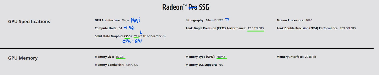
Please tell me how 36CUs@2.0GHz is gonna be economically cheaper to produce than 56CUs @1.675GHz.
Where did I say it is? Compared to 36CUs at 2.0GHz, it IS slow and something much more achievable and realistic in regards to NAVI. It is in general much more clockable than your Polaris cards.
Again where did I say this? Why are you resorting to lying?
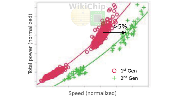
It is ironic you're lecturing me about power curve when I was the one to bring it into discussion as to how it affect yields. But yes, I do know. And, I also know, their dev kits are clocked at 1.8GHz and 2.0GHz which is way beyond NAVIs' sweet spot.
Besides, all your graphs using 5700/5700XT power curve is useless. You can't expect a console-level binned chip to perform close to a retail GPU. Why? Because of variance in silicon quality. Furthermore, concept of under-volting doesn't exist to console manufacturers. When AMD says 5700XT consumes maximum of 225W of power, that doesn't mean, ALL of 5700XT consume same amount of power. Some of them can achieve the same clocks at a lower-voltage, but that would be akin to winning a silicon raffle. These charts and graphs cannot be relied upon by console manufacturers to draw upon a baseline. But, this is something I've already explained to you earlier.
DF has stated XSX breaks what were traditional console barriers with regards to TDP, it's going to draw well north of 200W+. A look at form factor is a dead giveaway, so is Sonys' devkit.
Already told you how 7-10% won't be dramatic game-changer since the clock speeds of 1.8-2.0GHz are well beyond the optimum power/performance/thermal mark.
Yeah, these chips will magically start emitting much less heat, consume much less power after 18 month time-lapse just because node is more mature. Great argument.
Once again I never said that, you're again putting words in my mouth. I said why using 36CUs@1.8GHz would result in poor yields compared to a bigger GPU and gave you array of reasons as to why that would be the case. The reason which you have once again ignored.
Comparatively, comprehension is hard for some. Besides we have no idea if that is the configuration MS are going with for the Series X retail kit. They could opt for an even bigger CU count and further reduce the clocks to reach their target.
Such a shame I read this last or I wouldn't have wasted my energy. All the things I wrote about baseline, why companies divide tiers, how clocks and power affect yields etc. are chucked sideaways because 'I believe they can easily do that'.
Sigh, I give up. Carry on spreading your mis-information.