• Hey, guest user. Hope you're enjoying NeoGAF! Have you considered registering for an account? Come join us and add your take to the daily discourse.

Nintendo Switch Dev Kit Stats Leaked? Cortex A57, 4GB RAM, 32GB Storage, Multi-Touch.

Status
Not open for further replies.

LordOfChaos

Member
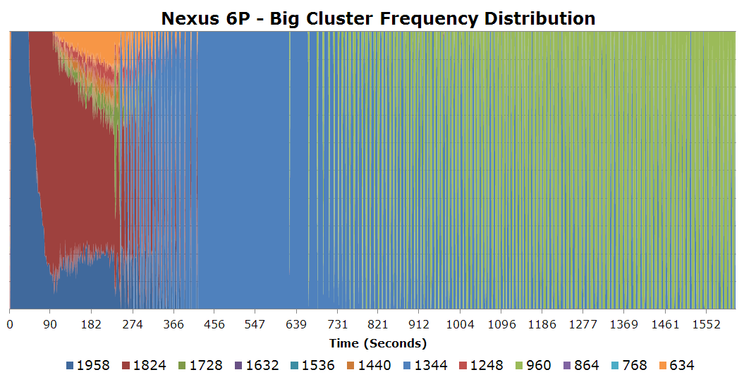
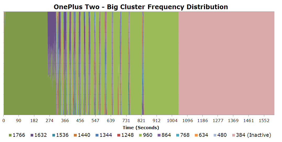
It's interesting to note that SoCs on high end Android phones can throttle to around or below 1GHz on the CPU:

6P (810)
6P.png


Oneplus Two
OP2.png


5X (S808)
5X.png


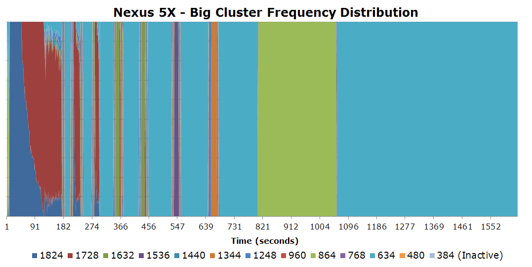
Granted the Snapdragon 810 was a particularly throttle happy SoC, the 820 was much better but I don't see this test done for it unfortunately, nor the TX1. And these aren't, of course, actively cooled like the Shield TV or Switch, and if they include heatsinks/heatspreaders they're tiny and phone sized.
 

MuchoMalo

Banned
I don't want to downplay it. I find the tests MDave does fascinating to follow. But what seemed to be quite a clear explanation at some point is back into speculation territory now.

What's interesting is that Pixel C has the CPU clock only a notch lower and the GPU clock cut down to almost Switch docked level. That would be interesting to see how it acts when it throttles.

You're basically saying that we either know everything or nothing. The size of the Switch is enough to explain why the CPU would need to be clocked lower in order to maintain the GPU clock. If you want perfect answers without any speculation whatsoever, you're going to have to wait for teardowns and a die analysis.
 

ggx2ac

Member
It's interesting reading about the GPU inside the iPad Air 2.

http://www.anandtech.com/show/8716/apple-a8xs-gpu-gxa6850-even-better-than-i-thought

A8X%20draft%20floorplan_575px.png


A8X SoC courtesy of Chipworks

However as we have theorized and since checked with other sources, GFXBench 3.0’s fillrate test is not bandwidth limited in the same way, at least not on Apple’s most recent SoCs. Quite possibly due to the 4MB of SRAM that is A7/A8/A8X’s L3 cache, this is a relatively “pure” test of pixel fillrate, meaning we can safely rule out any other effects.

With this in mind, normally Apple has a strong preference for wide-and-slow architectures in their GPUs. High clockspeeds require higher voltages, so going wide and staying with lower clockspeeds allows Apple to conserve power at the cost of some die space. This is the basic principle behind Cyclone and it has been the principle in Apple’s GPU choices as well. Given this, one could reasonably argue that A8X was using an 8 cluster design, but even with this data we were not entirely sure.

Clusters: 8, FP32 ALUs: 256, FP32 FLOPs/Clock: 512, FP16 FLOPs/Clock: 1024,Pixels/Clock (ROPs): 16, Texels/Clock :16

Meanwhile the die shot places the die size of A8X at roughly 128mm2.

Basically just showing how Apple went with a customised version of a PowerVR GX6650(?) which made the GPU larger to go with more power at low clocks to conserve battery power compared to running higher clock speeds.

The SoC had a 128-bit bus though using LPDDR3 RAM since this is older than a TX1.

I brought it up since the other article I posted where a TX1 was being compared to an iPad Air 2 mentioned this:

http://www.anandtech.com/show/8811/nvidia-tegra-x1-preview/3

The purpose of this demonstration was two-fold. First to showcase that X1 was up and running and capable of NVIDIA’s promised features. The second reason was to showcase the strong GPU performance of the platform. Meanwhile NVIDIA also had an iPad Air 2 on hand for power testing, running Apple’s latest and greatest SoC, the A8X. NVIDIA has made it clear that they consider Apple the SoC manufacturer to beat right now, as A8X’s PowerVR GX6850 GPU is the fastest among the currently shipping SoCs.

So the TX1 was designed to best Apple's SoC design, one of the big advantages was that the TX1 had memory bandwidth compression thanks to Maxwell that Nvidia went with a 64-bit bus and that LPDDR4 has a better bandwidth rate compared to LPDDR3.

None of this is suggesting anything about the Switch's possible specs, it's just to have a better understanding of mobile hardware related to the TX1 especially if you want to be thinking about what Nintendo could supposedly customise although we've gone through that a lot regarding fab node, bus width, number of SMs, RAM config, cache, CPU cores etc.
 

jackal27

Banned
Man this has GONE SOME PLACES

I can't even tell what I'm looking and all for a silly lil Captain Toad 2 console! This anticipation is real.

This is gonna be a loooooooong week til Thursday.
 

LordOfChaos

Member

Part of this is what I'm wondering/hoping/repeat-WUSTing. Given Nintendos history of making sure memory bandwidth isn't a primary developer pressure, I had wondered if like Apple, they would customize the Tegra with such an L3 cache, whether SRAM or eDRAM or eSRAM or whatever works, to alleviate memory pressure which is a long standing mobile weakness.

Or even have an external pool a-la Crystalwell. I get the feeling that if it was a separate chip like that we may have heard of it, but if it's additional memory on-die we'll find out with die scans (Anyone buddying up to Chipworks or Hector Marcan again yet?)

Nintendo had been very serious about the memory setup of their hardware since the disastrous setup in the N64, so it would be odd if they didn't make any customization for better efficiency.
 

ggx2ac

Member
Part of this is what I'm wondering/hoping/repeat-WUSTing. Given Nintendos history of making sure memory bandwidth isn't a primary developer pressure, I had wondered if like Apple, they would customize the Tegra with such an L3 cache, whether SRAM or eDRAM or eSRAM or whatever works, to alleviate memory pressure which is a long standing mobile weakness.

Memory bandwidth is basically the most I can expect customisation if any.

I'd be surprised if Nintendo added more CUDA cores since FP16 already helps in a sense to improve performance by some factor (but not exceeding 2x Flops) without having to increase GPU clock speed.

Other customisations? I don't know. I'd want to think they could have looked at A72 CPU cores but they'd really need to be 16nmFF to make a big difference in power consumption compared to A57.
 

Vic

Please help me with my bad english
Nintendo had been very serious about the memory setup of their hardware since the disastrous setup in the N64, so it would be odd if they didn't make any customization for better efficiency.
Actually, EVERY Nintendo hardware excepted the N64 had VRAM or some type of fast RAM. Even the NES and GB. The GBA was the first hardware with eSRAM in the main SoC IIRC. This is why it's very likely that the custom Tegra has a different internal and external memory setup from the X1. The biggest question mark regarding the GPU is what will be the amount of CUDA cores in the Switch SoC.
 

Vic

Please help me with my bad english
Memory bandwidth is basically the most I can expect customisation if any.

I'd be surprised if Nintendo added more CUDA cores since FP16 already helps in a sense to improve performance by some factor (but not exceeding 2x Flops) without having to increase GPU clock speed.

Other customisations? I don't know. I'd want to think they could have looked at A72 CPU cores but they'd really need to be 16nmFF to make a big difference in power consumption compared to A57.
If the fab process is indeed 20nm, it doesn't seem like anything other than A57 cores can be used.
 

Vena

Member
So both the A72 and A73 have 28nm designs, neat. (A57 and A53 as well.)

Too bad we've still heard absolutely nothing about the Switch CPU other than CPU clock speed on the dev kit and it being A57 since we know the dev kits were Jetson TX1.

It starts with an A. Heard it here first.
 

z0m3le

Banned
Nope, the CPU is hardly being used in that Unity test.

I managed to get the stats on the 3DMark benchmark when it appeared that the GPU was thermal throttling previously, large image warning:

http://puu.sh/tfUTW/8bb1f4b217.jpg

GPUs running max clock and not being pushed is quite different for heat consumption. Think of furmark and how they use to push cards into double tdp early on. So x1 running 990mhz when not being pushed isn't too important, if it was happening during heavy utilization, then we would have an issue. Thanks for all the hard work BTW.
 
Alrighty looks like the picture is starting to get clearer and clearer hah.

I ran my little indie game that pushes the CPU to 2GHz constantly, and rendering at 1080p 8xMSAA, getting about 30FPS with dips when CPU really gets hit a little too hard.


GPU is thermal throttling again! Even lower then 768MHz sometimes. Temperature is nearly 60c. But the CPU is staying a rock solid 2GHz. I guess that never throttles, so instead the Shield will throttle the GPU if the CPU starts heating things up. Which again lines up with the Dolphin developer, hah.

So in conclusion: GPU won't throttle down if the CPU is not being pushed to 2GHz. I don't know at what frequency it does start, but yeah interesting stuff.

About when the Physics test started running. Notice the massive dip in FPS shortly after the test started.
dumb question:
The Android TV you're testing, doesn't have a fan to cool the GPU and CPU, right? Sorry, dumb question for all the tech experts out there I'm sure. I'm trying to follow up on it as much as possible.

Its going to be a long week, but we likely won't know just how powerful switch is until sometime after March. /:
 

ggx2ac

Member
dumb question:
The Android TV you're testing, doesn't have a fan to cool the GPU and CPU, right? Sorry, dumb question for all the tech experts out there I'm sure. I'm trying to follow up on it as much as possible.

Its going to be a long week, but we likely won't know just how powerful switch is until sometime after March. /:

There's no fanless Shield TV.
 

Inuhanyou

Believes Dragon Quest is a franchise managed by Sony
Is this in relation to Sony and Microsoft's consoles? Just because Sony and Ms are cutthroat with their prices and undervalue gaming along with it, doesn't mean Nintendo isn't worth the price because it doesn't match it in raw specs. For a hybrid with a portability aspect with tech like this(not to mention rumored software at launch), the switch is worth the price at $250. Kimishima also has said he wants to make a profit of each console sold as well.

I hate when fans hook line and sinker regurgitate talking points of PR managers. That's exactly what Reggie said in regards to why the prices of their console and software don't go down.

Its a crappy argument as a consumer. You should want to get stuff as cheap as possible.

Nintendo knows this, they don't have a second back up plan in case this things goes south. They have to hit mass market balance right away. But that doesn't mean they are going to simply give these machines away just because they need to sell them. This 'undervaluing' mindset makes no sense.
 

Speely

Banned
For the techies:

Do you think that the NVN API and the libraries/tools that Nvidia has worked on will include any sort of automated testing tools for fp16 vs fp32 use and/or even some kind of driver settings that can convert some traditional fp32 code to fp16 based on heuristics, in order to sort of lay a basic framework before going in and manually switching shit around and then checking for artifacts, etc?

I am just thinking that for fp16 to be a considerable help with performance for ports, 3rd parties porting games would have a much easier time getting results if there were dedicated tools for that. As I understand it, mixed fp16 and fp32 code can be problematic if the coder is not taking specific care to avoid problems that can arise from it (catastrophic cancellation, namely,) and having dedicated tools for facilitating such mixed code usage would not only help devs avoid these pitfalls but also perhaps encourage them to use it in the first place. The Switch is after all supposed to make porting a fairly smooth process, in as much as it can be.

One concern of mine is that some devs will ignore fp16 code altogether. That's one reason I am happy that the PS4 Pro is around, since it won't just be exclusive to the Switch and PC, and might make what was once seen as retrogressive a bit more common among devs.
 
I hate when fans hook line and sinker regurgitate talking points of PR managers. That's exactly what Reggie said in regards to why the prices of their console and software don't go down.

Its a crappy argument as a consumer. You should want to get stuff as cheap as possible.

Nintendo knows this, they don't have a second back up plan in case this things goes south. They have to hit mass market balance right away. But that doesn't mean they are going to simply give these machines away just because they need to sell them. This 'undervaluing' mindset makes no sense.

Yes, I do think Publishers are devaluing videogames,, or certain companies are doing so out of desperation to continue profits and get a bigger install base.. When you have STEAM and subscriptions like PS+ and Xbox live giving out free games every month or at incredibly reduced prices, it cheapens the hard work developers put into the game and devalues them.

I never said we're not getting fantastic deals, nor am I trying to guilt tripping the actual consumers for buying these games and consoles for affordable prices. Indeed this is THE BEST time to be a consumer. If you adjust for inflation from the 90s, we're getting way better deals for games, and the games nowadays have a lot more content than they did back then.

Perhaps the real issue behind this is that the gaming industry is really volatile and it shows how risky and vulnerable gaming industry is as whole. They're bleeding. Games are more expensive than ever, and if you compare the industry now to 10 years ago, a lot of game developing companies have sent under. Now most of the AAA companies exist.

Anyway my point in that post you just quoted is just because sony and microsoft are making their consoles really affordable(and they ARE being cutthroat about it like a lot of big businesses are), doesn't mean the Switch is worth less at the same price when you compare it on raw power alone. I'm not saying that the PS4 and Xbone consoles themselves costing 250 is hurting the industry, just that sony and ms are really competitive(the devaluing is just the free games, wich I didn't mention in the post you quoted) I'm just tired of people saying things like the switch needs to be 200 because ps4 and xbone are 250 right now. I've always admired Nintendo for putting values into their games and consoles. Not all the time however--as the Wii U really should have dropped in price to 200-250 ages ago.

Other than that.. I'm not here for an extended discussion about this. This thread is supposed to be about discussing switch specs.

Yes, lets all be thankful to Nintendo for making us spend more than we need to, what sort of fanboy crap is that?

R&D for consoles should be much lower now than in the past since consoles are using customised off the shelf parts, gone are the days of expensive R&D where they are designing chips from scratch.

It's almost as bad as that thread thanking Nintendo for not reducing prices on their games years down the line.

Why would anyone be grateful that they have to spend more?

If studios are dying it's because their games just didn't sell that well, nothing to do with undervaluing gaming.
 

KingSnake

The Birthday Skeleton
You're basically saying that we either know everything or nothing.

Honestly I have no idea what are you talking about here. I guess you're doing a MuchoMalo but in the other direction.

The size of the Switch is enough to explain why the CPU would need to be clocked lower in order to maintain the GPU clock.

No, it doesn't. Especially since the new Shield is as small as Shield. What explains the CPU clock would be the power draw restrictions as mentioned already. That still doesn't fully explain the GPU clocks.

If you want perfect answers without any speculation whatsoever, you're going to have to wait for teardowns and a die analysis.

I don't want perfect answers. I actually like the speculations going on in this thread. I just said that the one version that looked to match much better the whole situation dropped and we're back to square one (as in there are several ideas, none having a clear advantage). For some reason this made you angry and I have no idea why? I didn't complain one bit about the speculations happening. Really. If you think otherwise you haven't paying attention.
 

ggx2ac

Member
No, it doesn't. Especially since the new Shield is as small as Shield. What explains the CPU clock would be the power draw restrictions as mentioned already. That still doesn't fully explain the GPU clocks.

20nm is a shitty node that leaks too much heat when doing work at high clock speeds.

Yes, the Shield TV CPU has a higher clock speed than the GPU, what is its wattage? Around 7.38W

What is the wattage of the GPU? Somewhere around 10W-12W but we know that is already throttled so it would actually be higher at 1GHz

Why would the GPU be throttling first then? It produces more voltage which causes more heat.

The cooling solution for the Shield TV isn't sufficient for it to run at 1GHz consistently, hence it throttles to 768 MHz which is almost a 25% drop in clock speed.

The TX1 can run at 1GHz GPU clock speed, it just needs a sufficient cooling solution.

The Shield TV doesn't list clock speeds in the specs page so they are not being misleading about clock speeds because they haven't listed any.
 

KingSnake

The Birthday Skeleton
20nm is a shitty node that leaks too much heat when doing work at high clock speeds.

Yes, the Shield TV CPU has a higher clock speed than the GPU, what is its wattage? Around 7.38W

What is the wattage of the GPU? Somewhere around 10W-12W but we know that is already throttled so it would actually be higher at 1GHz

Why would the GPU be throttling first then? It produces more voltage which causes more heat.

The cooling solution for the Shield TV isn't sufficient for it to run at 1GHz consistently, hence it throttles to 768 MHz which is almost a 25% drop in clock speed.

The TX1 can run at 1GHz GPU clock speed, it just needs a sufficient cooling solution.

The Shield TV doesn't list clock speeds in the specs page so they are not being misleading about clock speeds because they haven't listed any.

My point was that the GPU seems to throttle when the CPU is pushed to run at 2Ghz or close to that. If the CPU is already capped at 1Ghz, the GPU should not throttle anymore, as it seems to run perfectly fine in the Shield under these conditions (both CPU and GPU at 1Ghz) according to the tests.

So the throttling alone doesn't explain the GPU clock.

Of course it might be the case that the fan in Switch or the way Switch is organised on the inside to be less effective in terms of cooling than the Shield and then the GPU had to be also capped.
 

ggx2ac

Member
My point was that the GPU seems to throttle when the CPU is pushed to run at 2Ghz or close to that. If the CPU is already capped at 1Ghz, the GPU should not throttle anymore, as it seems to run perfectly fine in the Shield under these conditions (both CPU and GPU at 1Ghz) according to the tests.

So the throttling alone doesn't explain the GPU clock.

Of course it might be the case that the fan in Switch or the way Switch is organised on the inside to be less effective in terms of cooling than the Shield and then the GPU had to be also capped.

My assumption: MDave had the CPU and GPU at 1GHz so the GPU didn't throttle because the cooling was sufficient for the overall wattage. As we know, 4 A57 cores at 1GHz is around 1.8W so the 10W-12W GPU range increasing probably didn't put it over 20W total. Although if there was a way to get the Wattage measured with any of those benchmarks it would have been nice.

Why the CPU was acting weird during his test? I'm guessing the CPU clock speed was too low that it was a bottleneck for the benchmark test he was doing?
 
So, I just realized I'm off work Friday. The stream is @1pm Friday, right? (I'm in the same time zone as Kyoto)

I'm suddenly a lot more hyped than I should be...
 

MDave

Member
When I come home from work I will disable vsync so the GPU won't wait around for the next frame, now that I found the command to do that. One thing to be mindful of is that even if I force the CPU to 2GHz, if the load is still low/non-existant it won't throttle the GPU. 100% CPU load at 1GHz could still thermal throttle the GPU, but less likely to.
 

Mokujin

Member
My point was that the GPU seems to throttle when the CPU is pushed to run at 2Ghz or close to that. If the CPU is already capped at 1Ghz, the GPU should not throttle anymore, as it seems to run perfectly fine in the Shield under these conditions (both CPU and GPU at 1Ghz) according to the tests.

So the throttling alone doesn't explain the GPU clock.

Of course it might be the case that the fan in Switch or the way Switch is organised on the inside to be less effective in terms of cooling than the Shield and then the GPU had to be also capped.

You really don't need more explanation than 1Ghz being the balanced clock that.-


  • Is the sweet spot power consumption wise in handheld mode -> this clock is going to be the same docked to enable coherency between both modes.
  • Now that you have the CPU clock fixed you need the optimal GPU clock in handheld mode that gives a balanced performance / battery life combination, which might be those 307 Mhz.
  • From there you only need to upclock to a comfortable clock ratio that enables you to upgrade resolution to 1080 which a x2.5 jump is, some overhead over the x2.25 resolution jump.
This possible design choices chain leaves almost no room in my opinion to be puzzled about the clocks, and MDave testing further adds that there might be not much room left to upclock either side without getting into thermal problems (full cpu cluster + gpu + battery charge), there also might be some safety leeway to account for temperature deltas between regions, weather, etc. And that's also without really knowing how much power can Switch usb connection deliver, we know Dock max power but not how much goes to the main unit itself.

Of course there could still be arguing about using a better fab process or newer cores (i belive they are still a57s 20 nm until proven otherwise) but it wouldn't surprise me that even at 16nm if the chip has some noticeable customizations (cpu setup, memory setup, something weird?) those clocks would be the ones needed to balance the system.
 

Hermii

Member
You really don't need more explanation than 1Ghz being the balanced clock that.-


  • Is the sweet spot power consumption wise in handheld mode -> this clock is going to be the same docked to enable coherency between both modes.
  • Now that you have the CPU clock fixed you need the optimal GPU clock in handheld mode that gives a balanced performance / battery life combination, which might be those 307 Mhz.
  • From there you only need to upclock to a comfortable clock ratio that enables you to upgrade resolution to 1080 which a x2.5 jump is, some overhead over the x2.25 resolution jump.
This possible design choices chain leaves almost no room in my opinion to be puzzled about the clocks, and MDave testing further adds that there might be not much room left to upclock either side without getting into thermal problems (full cpu cluster + gpu + battery charge), there also might be some safety leeway to account for temperature deltas between regions, weather, etc. And that's also without really knowing how much power can Switch usb connection deliver, we know Dock max power but not how much goes to the main unit itself.

Of course there could still be arguing about using a better fab process or newer cores (i belive they are still a57s 20 nm until proven otherwise) but it wouldn't surprise me that even at 16nm if the chip has some noticeable customizations (cpu setup, memory setup, something weird?) those clocks would be the ones needed to balance the system.

It would be hilarious if they actually fit the Wii U cpu in a Tegra X1. Thats one of the crazier theories I seen here.
 

Mokujin

Member
It would be hilarious if they actually fit the Wii U cpu in a Tegra X1. Thats one of the crazier theories I seen here.

Yeah, I know it's crazy and I sure hope they don't do it, but after seeing what was inside Wii U MCM and the lengths they went just to have direct hardware BC plus those late Iwata comments I wouldn't even be surprised.

On a related note one of the later LKD comments saying that Gamecube VC games would not have upgraded resolution made me worried about being a hint toward this, but again I sure hope they made a fresh start this time for real.
 

Donnie

Member
Well I'd rather they have the WiiU CPU in there than just the 4 ARM cores alone. At least then they could use the WiiU CPU to run OS/secutiry stuff ect leaving all 4 ARM cores for games. Of course I'd much prefer they just kept the 4x A53 cores and modified the SoC to allow them to run at the same time as the higher power ARM cores.
 

FyreWulff

Member
Well I'd rather they have the WiiU CPU in there than just the 4 ARM cores alone. At least then they could use the WiiU CPU to run OS/secutiry stuff ect leaving all 4 ARM cores for games. Of course I'd much prefer they put 4x A53's in their for that.

this melts the handheld
 

Donnie

Member
What does? Modifying the SoC to allow the 4x A53 CPU to run along with the main ARM cores? It uses 0.5w for all four cores at full load at 1Ghz so no. Or are you talking about having a WiiU CPU in there? Well that uses about 4w on 45nm, on 20nm it'll use under 1w.
 

LordRaptor

Member
On a related note one of the later LKD comments saying that Gamecube VC games would not have upgraded resolution made me worried about being a hint toward this, but again I sure hope they made a fresh start this time for real.

Rightly or wrongly, Nintendo seem to value fidelity to the original experience with the VC, including darkened image outputs to reflect LCD screens being brighter than CRTs and 50Hz PAL titles to reflect much of their PAL output was poorly optimised for PAL displays.
 
Eh no the Wii U cpu will not be in there as they would need to both to pay NEC for the IP and use their process to manufacture the chip w/EDRAM (at 40 nm) so nope.


Edit: Also what FyreWulff said
 
Any possibility Nintendo adds more cores in the final version for the OS? They would have had to tell developers that they could only use 3 cores in their games otherwise right?
 

Donnie

Member
Any sort of PowerPC CPU. The Wii U needs a lot of airspace and a loud fan, in addition to the underclock, to keep temps under control.

Temperature management is one of the main reasons PowerPC deadended in consumer products.

Well obviously they wouldn't just chuck a entire WiiU SoC in their on a 45nm process like the original chip.. It would be just the 3x Espresso CPU cores inside the Switch SoC on the same 20nm process. Which would add maybe half a watt to the SoC, about the same extra power draw as 4x A53 cores.

Obviously I don't believe they'd do it anyway, but not because it would be any kind of issue for power draw. More because it would be a lot of bother modifying the SoC for a worse solution than just keeping the A53 cores and modifying them to run in tandem with the main ARM cores. I was just saying I'd rather have 3 Espresso cores in their than nothing.
 
Any possibility Nintendo adds more cores in the final version for the OS? They would have had to tell developers that they could only use 3 cores in their games otherwise right?

There is a possibility because the x1 in the shield TV has the following.

Tegra X1’s technical specifications include:
256-core Maxwell GPU
8 CPU cores (4x ARM Cortex A57 + 4x ARM Cortex A53)
60fps 4K video (H.265, H.264, VP9)
1.3 gigapixel of camera throughput
20nm process
 

Mokujin

Member
Eh no the Wii U cpu will not be in there as they would need to both to pay NEC for the IP and use their process to manufacture the chip w/EDRAM (at 40 nm) so nope.


Edit: Also what FyreWulff said


I can see other reasons that could make it a really difficult task, but those doesn`t look like a huge problem. But as I said just a crazy wild theory with some disturbing background, I also hope they just changed from cluster migration to global thread scheduling and took advantage of the a53 for the SO and extra working threads.

On a positive note we know that Nvidia has already done some work in the global thread scheduling design with Parker where Denver cores and A57s worked at the same time, so there is that.
 
Well yeah if you just chucked a WiiU CPU on its original 45nm process in there... But obviously in this case it would be WiiU CPU cores in the SoC on the same 20nm process. Which would add maybe half a watt to the SoC.

Obviously they aren't going to do it anyway, but it certainly wouldn't do anything like melt the handheld, it would add about the same extra power usage as 4x A53 cores.

Again I don't believe they'd do it anyway, just saying I'd rather have 3 Espresso cores in their than nothing.

You can't just shrink EDRAM and no-one has built any eDRAM on TSMCs process nodes at all. It's not just a case of shrinking it and hitting 'burn' on your foundry control panel. That's before we get into all the issues with multiple IP holders and the stratospheric cost of doing it even if it was available.

PowerPC is not a portable ISA none of the existing designs is optimised for on the go power consumption and IBM is deeply uninterested in adding them as their Power8 is all about HPC. Nintendo had to go with what is available and that is ARM
 
Well I'd rather they have the WiiU CPU in there than just the 4 ARM cores alone. At least then they could use the WiiU CPU to run OS/secutiry stuff ect leaving all 4 ARM cores for games. Of course I'd much prefer they just kept the 4x A53 cores and modified the SoC to allow them to run at the same time as the higher power ARM cores.

Why are we even discussing this... this is just absurd.. there is 0 chance this is happening.
 

Donnie

Member
You can't just shrink EDRAM and no-one has built any eDRAM on TSMCs process nodes at all. It's not just a case of shrinking it and hitting 'burn' on your foundry control panel. That's before we get into all the issues with multiple IP holders and the stratospheric cost of doing it even if it was available.

PowerPC is not a portable ISA none of the existing designs is optimised for on the go power consumption and IBM is deeply uninterested in adding them as their Power8 is all about HPC. Nintendo had to go with what is available and that is ARM

You don't have to have the eDRAM, the cache setup could be modified to share another cache on the SoC. Again I'm not saying they should do it, because their are far easier and better solutions. I said I'd rather have any extra CPU's on their than no extra CPU's even if it was a strange solution like 3x Espresso cores.
 

Donnie

Member
Why are we even discussing this... this is just absurd.. there is 0 chance this is happening.

We're discussing it because after someone mentioned the possibility I basically said that despite it being a bad idea I'd rather have any extra CPU's in their than no extra CPU's (even Espresso). It was then claimed it wouldn't be possible due to heat which isn't the case. But yeah its not going to happen, not because its impossible, because its a extremely strange thing to do. Hopefully they just keep the A53 cores and modify to allow them to run along with the main ARM cores.
 
You don't have to have the eDRAM, the cache setup could be modified to share another cache on the SoC. Again I'm not saying they should do it, because their are far easier and better solutions. I said I'd rather have any extra CPU's on their than no extra CPU's even if it was a strange solution like 3x Espresso CPU's.

When we start to do that we start to cause as many or more issues than just straight soft emulating Espresso. Timings would change which would require manual adjustments to either game code or to a s/w layer to sit on top and manage all of that somehow. To be honest I was shocked when WiiU continued down the PowerPC path at launch, it was always a technological dead end and left Nintendo stuck with a single supplier's tech that was never going to see a node shrink and thus the easy path to lower cost manufacture.

In fact the TX1 helps highlight some of these issues on it's own, despite shipping with a BIGlittle core setup only half the cores have ever been enabled in shipping solutions. The long standing rumour has been that cache coherency between the two four core modules is broken. Without cache coherency it's impossible for the two modules to share workloads without expensive and disastrously slow flush to RAM so everyone just fuses one or other module off. I'm very curious to see if Switch will completely excise these vestigial cores or will they just fuse them off as everyone else has.
 

Donnie

Member
Oh I agree its a ridiculous solution to a simple problem. I was just trying to make the point that I hope there are more than just the four main cores no matter what is used. There needs to be something to run the OS and leave all four main cores for gaming, or developers may run into real problems.

No idea why TX1 can't use both sets of CPU's at the same time, I haven't looked into it. Hopefully its something Nintendo have had Nvidia work on. Because while the likes of Shield and Pixel C might have a use for switching to a low power CPU at times a games system doesn't really. Also having all 8 cores work at once would be a great advantage for such a small amount of extra power draw.
 
We're discussing it because after someone mentioned the possibility I basically said that despite it being a bad idea I'd rather have any extra CPU's in their than no extra CPU's (even Espresso). It was then claimed it wouldn't be possible due to heat which isn't the case. But yeah its not going to happen, not because its impossible, because its a extremely strange thing to do. Hopefully they just keep the A53 cores and modify to allow them to run along with the main ARM cores.

Ya it seems more likely they include the shield tv setup of 8 CPU cores (4x ARM Cortex A57 + 4x ARM Cortex A53). That would be nice if they do it.
 
Status
Not open for further replies.
Top Bottom