• Hey, guest user. Hope you're enjoying NeoGAF! Have you considered registering for an account? Come join us and add your take to the daily discourse.

Nintendo Switch Dev Kit Stats Leaked? Cortex A57, 4GB RAM, 32GB Storage, Multi-Touch.

Status
Not open for further replies.
When we start to do that we start to cause as many or more issues than just straight soft emulating Espresso. Timings would change which would require manual adjustments to either game code or to a s/w layer to sit on top and manage all of that somehow. To be honest I was shocked when WiiU continued down the PowerPC path at launch, it was always a technological dead end and left Nintendo stuck with a single supplier's tech that was never going to see a node shrink and thus the easy path to lower cost manufacture.

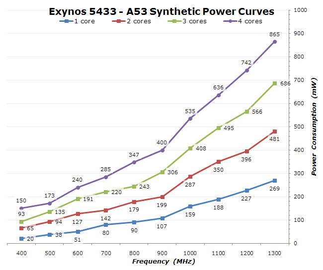
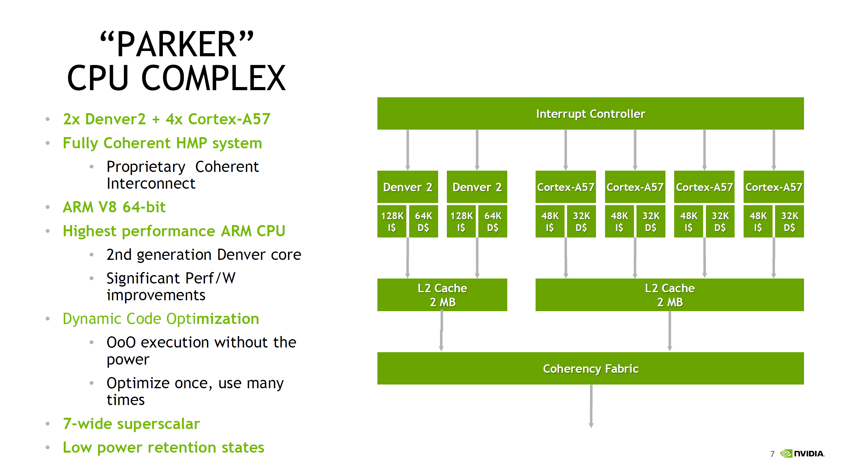
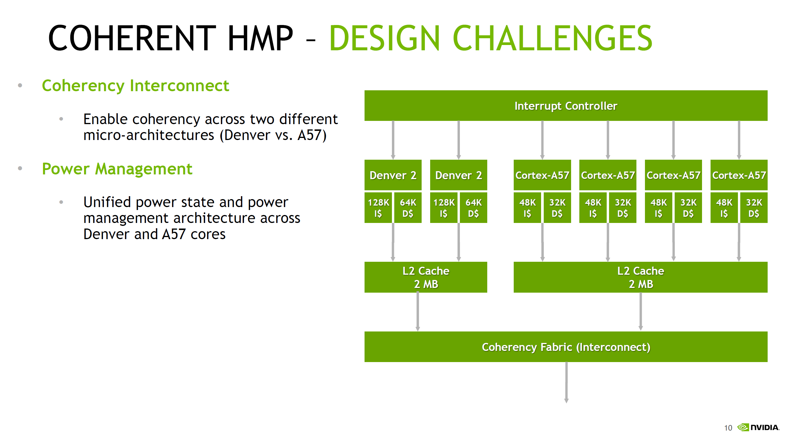
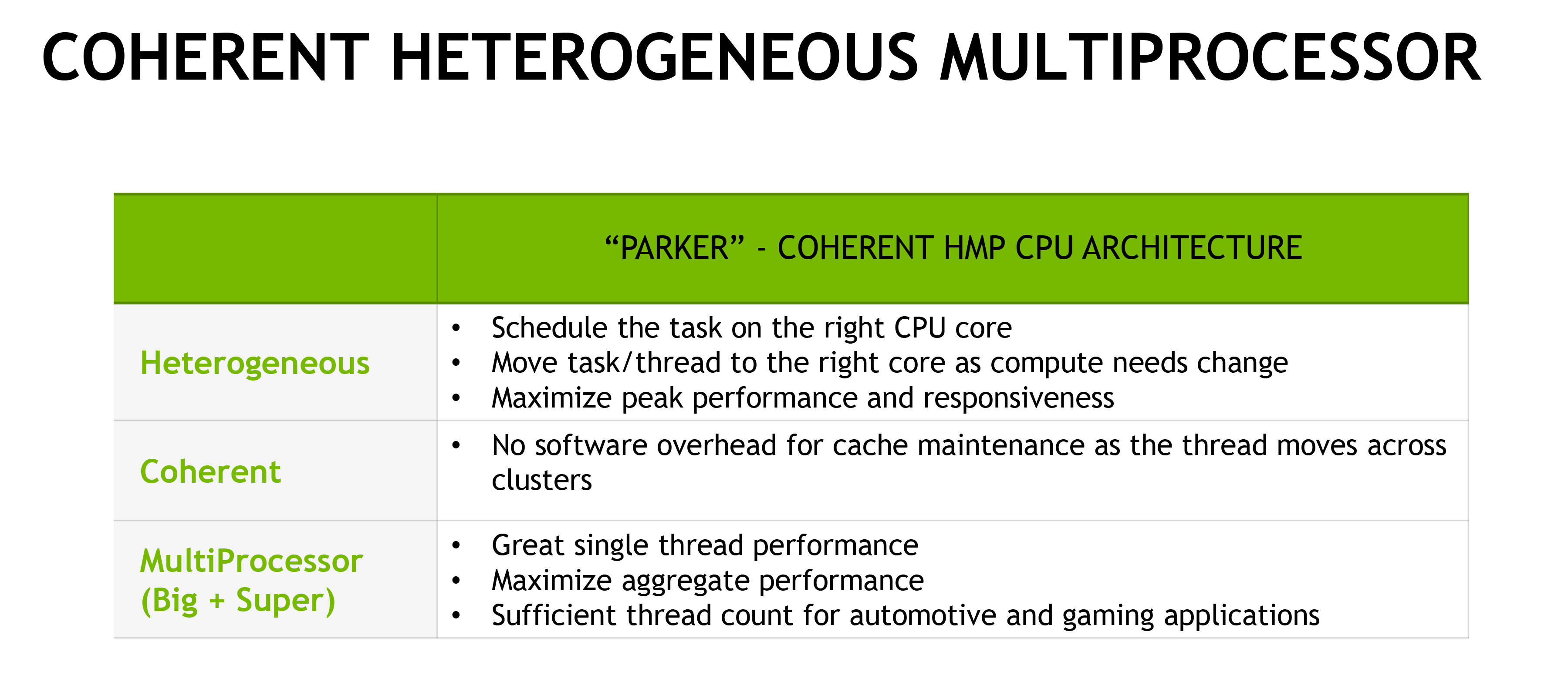
In fact the TX1 helps highlight some of these issues on it's own, despite shipping with a BIGlittle core setup only half the cores have ever been enabled in shipping solutions. The long standing rumour has been that cache coherency between the two four core modules is broken. Without cache coherency it's impossible for the two modules to share workloads without expensive and disastrously slow flush to RAM so everyone just fuses one or other module off. I'm very curious to see if Switch will completely excise these vestigial cores or will they just fuse them off as everyone else has.

Couldn't OS threads run rather independently from games though? Calls to the API could theoretically run directly on the big cores, while background threads run on the little cores.
 
The question is how hard would it be to modify the SoC to allow the A57 and A53 cores to run simultaneously?

Quite difficult, if it had been trivial then NV would have done so by now because it is a major issue for phone and tablet designs that benefit from BIG.little designs. On a recent investor con-call they said they had no 'custom' cpu design work on the go right now which suggests that the Switch TX1 is pretty close to standard TX1. Now perhaps there were NDAs in place but being 'flexible' with the truth in investor con calls is frowned upon pretty hard. We likely won't know if any custom work has been done until someone gets a switch, laps the CPU and throws it under a scanning electron microscope

Couldn't OS threads run rather independently from games though? Calls to the API could theoretically run directly on the big cores, while background threads run on the little cores.

No as they share a memory controller, without cache coherency when Module A wants to read Address X Module B has to flush all of it's cache and registers to RAM to ensure it hasn't taken the data at X and modified it somehow which stalls Module B and A while this happens. Without fixing cache coherency it is practically impossible to use both modules
 

Schnozberry

Member
The question is how hard would it be to modify the SoC to allow the A57 and A53 cores to run simultaneously?

It wouldn't be the same processor at all. As it is, they share logic. They'd have to move to a two cluster setup with heterogeneous multiprocessing and coherent cache.
 

Mr Swine

Banned
It wouldn't be the same processor at all. As it is, they share logic. They'd have to move to a two cluster setup with heterogeneous multiprocessing and coherent cache.

Can't they just put in 8 A57 cores in there and scrap the A53 cores or would that not be feasible at all?
 

Mokujin

Member
Quite difficult, if it had been trivial then NV would have done so by now because it is a major issue for phone and tablet designs that benefit from BIG.little designs. On a recent investor con-call they said they had no 'custom' cpu design work on the go right now which suggests that the Switch TX1 is pretty close to standard TX1. Now perhaps there were NDAs in place but being 'flexible' with the truth in investor con calls is frowned upon pretty hard. We likely won't know if any custom work has been done until someone gets a switch, laps the CPU and throws it under a scanning electron microscope

While I'm not saying its the case, as I commented above Nvidia has already done work in this field as seen in these Parker Slides.-

Parker4.PNG

Not saying it's the case, and of course not relating Parker at all with Switch, but seems like if Nintendo wanted and Nvidia tried they could make A57s and A53s work together.

Anandtech
 

Schnozberry

Member
Can't they just put in 8 A57 cores in there and scrap the A53 cores or would that not be feasible at all?

They could do whatever they want. If they wanted more threads, they'd probably be better off with 8 A53 cores at higher clocks, because their power consumption is so low it's almost magical.
 

AlStrong

Member
Can't they just put in 8 A57 cores in there and scrap the A53 cores or would that not be feasible at all?

A57s are significantly larger per core, and then there's associated L2 cache, which is also a fair bit more.

Then there's the power consumption.
 
While I'm not saying its the case, as I commented above Nvidia has already done work in this field as seen in these Parker Slides.-
...
Not saying is the case, and of course not relating Parker at all with Switch, but seems like if Nintendo wanted and Nvidia tried they could make A57s and A53s work together.

Absolutely they could but at this point the costs start to spiral in a very bad way. Building on TX1, even with it's limitations, works for Nintendo as it is a mature product with good docs and known performance parameters. Building a solution on TX1 works for NV because they need to recoup the investment in it's creation and it gives them a high/low product mix. Nintendo gets a stable product at lower cost, NV gets someone to feed them an ongoing revenue stream to allow them to try and find high margin customers for Parker.
 
What I would say is "nothing" is off the table. As much hate as Nintendo gets for being "cheap" they don't mind spending money to customize the processors for their consoles. If I recall from the WiiU GPU thread someone that worked at Renesas said it was pretty expensive to create the GPU in the Wii U. So I say we wait and either Nvidia decides to give us more info at the event or some time this week or we E wait for a system teardown.

It was from chipworks
Originally Posted by Jim Morrison, Chipworks

Been reading some of the comments on your thread and have a few of my own to use as you wish.

1. This GPU is custom.
2. If it was based on ATI/AMD or a Radeon-like design, the chip would carry die marks to reflect that. Everybody has to recognize the licensing. It has none. Only Renesas name which is a former unit of NEC.
3. This chip is fabricated in a 40 nm advanced CMOS process at TSMC and is not low tech
4. For reference sake, the Apple A6 is fabricated in a 32 nm CMOS process and is also designed from scratch. It’s manufacturing costs, in volumes of 100k or more, about $26 - $30 a pop. Over 16 months degrade to about $15 each
a. Wii U only represents like 30M units per annum vs iPhone which is more like 100M units per annum. Put things in perspective.
5. This Wii U GPU costs more than that by about $20-$40 bucks each making it a very expensive piece of kit. Combine that with the IBM CPU and the Flash chip all on the same package and this whole thing is closer to $100 a piece when you add it all up
6. The Wii U main processor package is a very impressive piece of hardware when its said and done.
 

Mokujin

Member
Absolutely they could but at this point the costs start to spiral in a very bad way. Building on TX1, even with it's limitations, works for Nintendo as it is a mature product with good docs and known performance parameters. Building a solution on TX1 works for NV because they need to recoup the investment in it's creation and it gives them a high/low product mix. Nintendo gets a stable product at lower cost, NV gets someone to feed them an ongoing revenue stream to allow them to try and find high margin customers for Parker.

Eh I'm the first one defending that the Switch SoC is going to be very, very close to a standard TX1 but if there has been some customization that doesn't seem like a big deal to me (plus there are already other SoCs in the market already using A57s + A53s with global thread scheduling).
 

MuchoMalo

Banned
I wanted to estimate how much of a boost in "instructions per FLOPS" we're looking at going from R700 (the basis of Wii U's GPU) to Maxwell. To do this, I used the 3DMark Vantage graphics scores of the Radeon HD 4870 at stock (1.2 TFLOPS) and the GTX 980 Ti @1.274GHz (7.175 TFLOPS). From this comparison, you can see that the 980 Ti is 8.7x as fast as the 4870 in this test, but only 6x as fast in terms of FLOPS. This works out to an "IPFLOPS" advantage of 1.45x in Maxwell's favor. Thus, scaled back to the efficiency of Wii U's GPU, the Switch in handheld mode is as powerful as 228 GFLOPS version of the Wii U's GPU, or roughly 30% faster than Wii U. In docked mode this becomes 570 scaled GFLOPS 3.2x as fast as Wii U.

I want to note though that this isn't consistent across the line; when I used a 750 Ti instead of the 980 Ti the advantage jumped to 1.66x, meaning the portable and docked clocks of Switch would be 1.48x and 3.71x as powerful as Wii U respectively. It's probably somewhere inbetween, but only when not using FP16. Nintendo themselves will probably try to use it as much as possible, so 1.5-2x Wii U in handheld mode is likely what we'll see from Nintendo in real-world usage (though trying to quantify that by eye is difficult/impossible and to many people it'll still just seem like a portable Wii U that can render in 1080p on a TV).

Should I do something similar to compare GCN 1.1 (Xbone) to Switch?
 

foltzie1

Member
What I would say is "nothing" is off the table. As much hate as Nintendo gets for being "cheap" they don't mind spending money to customize the processors for their consoles. If I recall from the WiiU GPU thread someone that worked at Renesas said it was pretty expensive to create the GPU in the Wii U. So I say we wait and either Nvidia decides to give us more info at the event or some time this week or we E wait for a system teardown.

A PowerPC CPU being on die with an ARM chipset probably is off the table. An AMD GPU sharing on die with an Nvidia GPU is probably off the table.

You are right we won't "know" with 100% certainty until Thursday, but I would be willing to make a beefy wager it won't be.

Anyone want to make an avatar bet on the subject?
 
It is just going to be the x1 soc with a few modifications to clock speed and how the memory is handled. Further customization could come from the fab process as well.

I go with the most simple path.. They dont want to reinvent the wheel they want to get out a cost effective solution so this thing can be in as many hands as possible as fast as possible.

People are getting too cute on what is going in this thing.
 
Exactly. So basically I always hated the Nintendo cheaps out every time stigma. You can argue their reasons but a lot of people are going off the assumption Nintendo is trying to cheap out and using close to standard tx1. I say we wait they obviously did something pretty amazing to have this thing running the full version of unreal 4 at medium setting assuming all of that is true. But I like you guys can't wait to see what they did. I think they worked some magic along with Nvidia to create a pretty special chipset in the switch.

Agreed, I dunno what to expect about this system from the technical side, but when you see ps4 ports on the vita(I found the downgrade was huge on some games) and everyone saying that it will be the difference between the vita and 360 technically, well maybe who know but visually I guess there could be some "magic" and giving the feeling of a "portable current gen" if you compare it to a ps4 or xbox one(even the difference could become really clear in docked mode) thanks to the optimization that Nvidia + Nintendo have worked on.
I'm confident that we will not have a vita render in current gen ports, and the vita gave illusion to have a "ps3 handheld" in our hands.
 
Exactly. So basically I always hated the Nintendo cheaps out every time stigma. You can argue their reasons but a lot of people are going off the assumption Nintendo is trying to cheap out and using close to standard tx1. I say we wait they obviously did something pretty amazing to have this thing running the full version of unreal 4 at medium setting assuming all of that is true. But I like you guys can't wait to see what they did. I think they worked some magic along with Nvidia to create a pretty special chipset in the switch.
While Nintendo didn't "cheap out" with the Wii U, that also drove up the price, which is something we know they're trying to avoid this time.
 

Hermii

Member
I think what needs to be looked at is this is a rebranding and a restart for nintendo. Their main guy died last year, they have all their devs working on one platform, and they are moving away from an old architecture. This chip is not being made with just switch in mind. They are thinking about years after the switch. Think gamecube they designed those chips and got three consoles selling a total of 136 million. But again we will see. Hopefully we can get better info from Nvidia.

I think you are right there, except for the part about Iwata I don't think that has anything to do with it. I think Iwata wanted a restart with the switch, looking at things he said.

I think this chip or perhaps even more the NVN API is created for the long term. I think any game written in NVN will work natively on all future Nintendo hardware for as long as they are partnered with NVIDIA. They can probably release a much more powerful Volta switch in a few years and have perfect bc with the Switch.
 

Vena

Member
They aren't putting a WiiU inside the Switch. They also aren't running a stock TX1 at lower clocks with all else equal.

I'd put my money on:
  • Memory changes (L3 cache, or large cahce, or bus-speed changes)
  • Tore out the A53 cores, or they are used to run the OS/Record
  • Final clocks were likely tested at their utmost limits for thermal throttling.
I think the fact that they clocked up their dev-kits sometime near the end of last year may actually mean they made significant changes to the chip, since I'd imagine that the TX1 throttle is actually more lenient (in the old Shield TV, IIRC it is larger+thicker than the Switch). If they managed to get it higher later in life, this could be from a shrink to 16nm transition that came in later on and allowed the final kits to clock higher to match retail.

OG SHIELD TV:
Depth: 25mm

NS:
Depth: ~14mm

If we take all else being equal, I think its not unreasonable that they may well have shrunk the Maxwell to 16nm, grabbed some aspects of Parker, and called it a day. This gives them comparable clocks to the TX1 in the OG Shield TV but in a smaller unit, lower wattage needs, and longer battery (fits in with Laura and Nate's updated times on battery power... or they have some gargantuan battery pack).

Given the depth shrink, and the seeming inefficacy of the thermal conduction for the TX1 to maintain its clocks in the larger shell, either Nintendo added a really potent fan for a smaller casing or their chip is more efficient to remain at the peak throttle of the TX1 while also charging a battery (which also introduces heat).
 
I think you are right there, except for the part about Iwata I don't think that has anything to do with it. I think Iwata wanted a restart with the switch, looking at things he said.

I think this chip or perhaps even more the NVN API is created for the long term. I think any game written in NVN will work natively on all future Nintendo hardware for as long as they are partnered with NVIDIA. They can probably release a much more powerful Volta switch in a few years and have perfect bc with the Switch.

That would be awesome!
 

LordOfChaos

Member
It would be hilarious if they actually fit the Wii U cpu in a Tegra X1. Thats one of the crazier theories I seen here.

Hah, if the trusty old PowerPC 750 lived on for another half decade in a Nintendo console, I wouldn't know to laugh or cry...

Since they never said it's BC I think we can safely discount that theory...I hope...

Nvidia: "So we have this cool modernish SoC"
Nintendo: "Mmhmm"
"It's GPU architecture is broadly compatible with the rest of the 2017 world"
Nintendo: "OK"
Nvidia: "It has modern A57 cores and DSP and NEON SIMD per core"
Nintendo: "Hold on...Can we put the iMac G3 processor in there?"
Nvidia: ಠ_ಠ


Any sort of PowerPC CPU. The Wii U needs a lot of airspace and a loud fan, in addition to the underclock, to keep temps under control.

Temperature management is one of the main reasons PowerPC deadended in consumer products.


Underclock? The Espresso in the Wii U is maybe the second highest clocked the 750 has ever been, the GPU is what was underclocked from the rumour. The PowerPC CPU would have been a pretty small part of the already small power draw, suggesting "any PowerPC CPU" is a heat monster is a very broad stroke. The POWER series, certainly, but PowerPC is just an ISA, you can scale up, you can scale down, and the 750 on a modern process proved small and power efficient.

It's just lacking in some modernities, has nothing like ARMs Advanced SIMD or much in the way of branch prediction, etc. If the fan is loud in a 30W TDP, that's Nintendos design and system budget.
 

Thraktor

Member
It wouldn't be the same processor at all. As it is, they share logic. They'd have to move to a two cluster setup with heterogeneous multiprocessing and coherent cache.

Cache coherency shouldn't be that big of a deal if the clusters are operating on separate data sets (i.e. the big cores on games and the small cores on the OS), but yeah, they would have to use a different setup than the TX1 to even make all 8 cores useable at the same time anyway. I'd be kind of surprised if they weren't using A53s for the OS, given how they'd do the job within a near-trivial die area and power consumption compared to big ARM cores like A57/A72.

Speaking of ARM cores, it's worth noting that the recently announced Snapdragon 835 uses customised ARM Cortex cores rather than the fully custom cores Qualcomm used in the 820. I'm not really expecting anything other than stock cores in Switch's SoC, but if Nvidia are going this route with their new cores I suppose it's possible that we could get something lightly modified in Switch.
 

Thraktor

Member
You mean like Denver? :p

Yep, good old "lightly modified Cortex core" Denver. It's basically just an A57 if you scrap everything about it down to the ISA itself.

I'm assuming that for the "custom ARM64 CPU" in Xavier they're dropping the Denver design in favour of a native ARM core, but it's still likely to be too far away to be used in Switch.
 
I wanted to estimate how much of a boost in "instructions per FLOPS" we're looking at going from R700 (the basis of Wii U's GPU) to Maxwell. To do this, I used the 3DMark Vantage graphics scores of the Radeon HD 4870 at stock (1.2 TFLOPS) and the GTX 980 Ti @1.274GHz (7.175 TFLOPS). From this comparison, you can see that the 980 Ti is 8.7x as fast as the 4870 in this test, but only 6x as fast in terms of FLOPS. This works out to an "IPFLOPS" advantage of 1.45x in Maxwell's favor. Thus, scaled back to the efficiency of Wii U's GPU, the Switch in handheld mode is as powerful as 228 GFLOPS version of the Wii U's GPU, or roughly 30% faster than Wii U. In docked mode this becomes 570 scaled GFLOPS 3.2x as fast as Wii U.

I want to note though that this isn't consistent across the line; when I used a 750 Ti instead of the 980 Ti the advantage jumped to 1.66x, meaning the portable and docked clocks of Switch would be 1.48x and 3.71x as powerful as Wii U respectively. It's probably somewhere inbetween, but only when not using FP16. Nintendo themselves will probably try to use it as much as possible, so 1.5-2x Wii U in handheld mode is likely what we'll see from Nintendo in real-world usage (though trying to quantify that by eye is difficult/impossible and to many people it'll still just seem like a portable Wii U that can render in 1080p on a TV).

Should I do something similar to compare GCN 1.1 (Xbone) to Switch?

I think that is a nice idea as long as you continue to look at more than one sample to make a conclusion. Your results so far seems to be roughly around what would be expected.

If you have the time, you can play around with another comparison. If anything, it is something to check out as we wait for the 12th. :)
 

Schnozberry

Member
Cache coherency shouldn't be that big of a deal if the clusters are operating on separate data sets (i.e. the big cores on games and the small cores on the OS), but yeah, they would have to use a different setup than the TX1 to even make all 8 cores useable at the same time anyway. I'd be kind of surprised if they weren't using A53s for the OS, given how they'd do the job within a near-trivial die area and power consumption compared to big ARM cores like A57/A72.

Speaking of ARM cores, it's worth noting that the recently announced Snapdragon 835 uses customised ARM Cortex cores rather than the fully custom cores Qualcomm used in the 820. I'm not really expecting anything other than stock cores in Switch's SoC, but if Nvidia are going this route with their new cores I suppose it's possible that we could get something lightly modified in Switch.

It really seems like Nintendo found themselves planning the Switch at a disadvantage. Had the WiiU been more successful, they would have had the luxury of perhaps waiting another year and finding themselves with much better technology to work with.
 

AlStrong

Member
Yep, good old "lightly modified Cortex core" Denver. It's basically just an A57 if you scrap everything about it down to the ISA itself.

I'm assuming that for the "custom ARM64 CPU" in Xavier they're dropping the Denver design in favour of a native ARM core, but it's still likely to be too far away to be used in Switch.

I meant, it didn't seem like nV was going for a light modification direction.
 
It really seems like Nintendo found themselves planning the Switch at a disadvantage. Had the WiiU been more successful, they would have had the luxury of perhaps waiting another year and finding themselves with much better technology to work with.
The concept of the Wii U in general was a little too early for it to properly work the way it should to make it marketable. Technology marches on, but at least there is the concept of the Switch can work well with what is available today. It can be improved in later renditions.
 

MuchoMalo

Banned
I think that is a nice idea as long as you continue to look at more than one sample to make a conclusion. Your results so far seems to be roughly around what would be expected.

If you have the time, you can play around with another comparison. If anything, it is something to check out as we wait for the 12th. :)

The issue is that there aren't too many ways to make such a comparison without buying a 4870 and testing it against my GTX 970 in a few DX10 games. With that said, DX10 is a huge factor here, as the difference may not be the same due to huge API differences.

What I will say is that this is the second comparison I've done, but I don't have the results from the first one saved anywhere.
 

MDave

Member
Oh man, this is interesting. The CPU is definitely throttling the GPU when its at 2GHz. And it looks like the other way around is true too.

Here are the results when I don't lock the CPU to any frequency, the kernel / governor manages it all:

These are the best results. This is also when the GPU went as low as 768MHz when it was, I suspect, it being throttled.

https://puu.sh/tfUTW/8bb1f4b217.jpg

Here are the results of locked 2GHz CPU benchmarks. Notice it has actually performed worse then a non-locked CPU frequency! The GPU sometimes goes as low as 537MHz.

http://puu.sh/tgLof/19520ff241.jpg
http://puu.sh/tgLJs/dd2570df40.png

And this is the results when the CPU is locked at 1GHz. The GPU is able to stay much closer to 1GHz. But it looks like the GPU might be thermal throttling the CPU, as the CPU can't keep a lock at 1GHz for some reason.

http://puu.sh/tgLGp/0c42f6c426.jpg
http://puu.sh/tgLLw/deb8b6bbe1.png

It's looking like the CPU and GPU cannot operate at their maximum frequencies when both are pushed as hard as they can at the same time. So to get the most out of it, best to develop a game that doesn't push the CPU too hard to get the most out of the GPU, and vice versa :p

Lastly, it's not simple to turn off vsync after all. Looks like Android relies on it at a core level.
 

blu

Wants the largest console games publisher to avoid Nintendo's platforms.
Oh man, this is interesting. The CPU is definitely throttling the GPU when its at 2GHz. And it looks like the other way around is true too.

Here are the results when I don't lock the CPU to any frequency, the kernel / governor manages it all:

These are the best results. This is also when the GPU went as low as 768MHz when it was, I suspect, it being throttled.

https://puu.sh/tfUTW/8bb1f4b217.jpg

Here are the results of locked 2GHz CPU benchmarks. Notice it has actually performed worse then a non-locked CPU frequency! The GPU sometimes goes as low as 537MHz.

http://puu.sh/tgLof/19520ff241.jpg
http://puu.sh/tgLJs/dd2570df40.png

And this is the results when the CPU is locked at 1GHz. The GPU is able to stay much closer to 1GHz. But it looks like the GPU might be thermal throttling the CPU, as the CPU can't keep a lock at 1GHz for some reason.

http://puu.sh/tgLGp/0c42f6c426.jpg
http://puu.sh/tgLLw/deb8b6bbe1.png

It's looking like the CPU and GPU cannot operate at their maximum frequencies when both are pushed as hard as they can at the same time. So to get the most out of it, best to develop a game that doesn't push the CPU too hard to get the most out of the GPU, and vice versa :p

Lastly, it's not simple to turn off vsync after all. Looks like Android relies on it at a core level.
Thank you, MDave, for the in-depth clock work. Apropos, can you build NDK code for it, seeing how gaf is largely short of A57 boxes ; )
 

MuchoMalo

Banned
Oh man, this is interesting. The CPU is definitely throttling the GPU when its at 2GHz. And it looks like the other way around is true too.

Here are the results when I don't lock the CPU to any frequency, the kernel / governor manages it all:

These are the best results. This is also when the GPU went as low as 768MHz when it was, I suspect, it being throttled.

https://puu.sh/tfUTW/8bb1f4b217.jpg

Here are the results of locked 2GHz CPU benchmarks. Notice it has actually performed worse then a non-locked CPU frequency! The GPU sometimes goes as low as 537MHz.

http://puu.sh/tgLof/19520ff241.jpg
http://puu.sh/tgLJs/dd2570df40.png

And this is the results when the CPU is locked at 1GHz. The GPU is able to stay much closer to 1GHz. But it looks like the GPU might be thermal throttling the CPU, as the CPU can't keep a lock at 1GHz for some reason.

http://puu.sh/tgLGp/0c42f6c426.jpg
http://puu.sh/tgLLw/deb8b6bbe1.png

It's looking like the CPU and GPU cannot operate at their maximum frequencies when both are pushed as hard as they can at the same time. So to get the most out of it, best to develop a game that doesn't push the CPU too hard to get the most out of the GPU, and vice versa :p

Lastly, it's not simple to turn off vsync after all. Looks like Android relies on it at a core level.

And now we have our answers for the chosen clocks. The CPU is clocked as low as it is for the sake of keeping power consumption low, and the GPU ios clocked where it is because retaining the max clock 100% of the time simply isn't possible without more cooling and stronger power delivery. The undocked GPU clock was chosen due to how it performs next to Wii U (being a GCN -> Wii kind of jump except with much bigger improvements beneath the surface) and because Nintendo likely wants all of their own games to run at native 720p on the go and native 1080p at home with identical settings otherwise. It all adds up. Thus, we can say that the Tegra within the Switch is identical to the X1 in almost every way except clock speeds as far as the CPU and GPU go. The customization, if any, was likely done elsewhere; I'd assume to mitigate the bandwidth issue or, worse, to simply remove the A53 cores meaning that only 2-3 cores would be usable by games unless the OS doesn't run in the background at all.
 

KingV

Member
Interesting thread. Though switch isn't probably hitting the speculation of the early days, it still looks like a pretty cool system given the portability.

A portable Wii U that hits 1080p when docked is damn nice compared to a 3ds or Vita.
 

Thraktor

Member
It really seems like Nintendo found themselves planning the Switch at a disadvantage. Had the WiiU been more successful, they would have had the luxury of perhaps waiting another year and finding themselves with much better technology to work with.

Well, yeah, 10/7nm and A73s and Volta and so forth would be nice, but there's always better technology around the corner. The most important thing for Switch technologically is that they set themselves up in a way that gives them the greatest possible latitude when developing future hardware while retaining compatibility, and they're actually in a good spot for that, with technology like ARMv8 and Vulkan giving them the ability to target a wide variety of performance levels and form-factors (and potentially even CPU/GPU vendors) going forward. Being able to use Maxwell/Pascal, the first desktop-class GPU arch in a long time to use tiled rendering, is also very helpful in that it allows them to do away with their usual route of using a big pool of (expensive) on-die VRAM in favour of a unified single memory pool.

I meant, it didn't seem like nV was going for a light modification direction.

Well, yes, they didn't go the light modification route for Denver, but that's not necessarily an indication of what they're going to do in the future. (For one thing Denver's design was of course heavily influenced by the desire to run both ARM and x86, and even then it seems to be largely based on Transmeta's work, so isn't necessarily a ground-up design.) If Qualcomm, a company which probably has the second-highest ARM R&D spend after Apple, is backtracking on a fully custom design to use a modified Cortex instead, then what's to say Nvidia won't do the same? Perhaps using a modified Cortex for the first generation or two of their post-Denver core before moving to a fully custom core.

Anyway, I don't think Nintendo's actually getting a custom CPU (except perhaps some light cache modifications or something like that), I just find it kind of interesting that Qualcomm is moving closer to ARM's reference designs, particularly in the context of what Nvidia will be doing for both Switch and Xavier.
 
Oh man, this is interesting. The CPU is definitely throttling the GPU when its at 2GHz. And it looks like the other way around is true too.

Here are the results when I don't lock the CPU to any frequency, the kernel / governor manages it all:

These are the best results. This is also when the GPU went as low as 768MHz when it was, I suspect, it being throttled.

https://puu.sh/tfUTW/8bb1f4b217.jpg

Here are the results of locked 2GHz CPU benchmarks. Notice it has actually performed worse then a non-locked CPU frequency! The GPU sometimes goes as low as 537MHz.

http://puu.sh/tgLof/19520ff241.jpg
http://puu.sh/tgLJs/dd2570df40.png

And this is the results when the CPU is locked at 1GHz. The GPU is able to stay much closer to 1GHz. But it looks like the GPU might be thermal throttling the CPU, as the CPU can't keep a lock at 1GHz for some reason.

http://puu.sh/tgLGp/0c42f6c426.jpg
http://puu.sh/tgLLw/deb8b6bbe1.png

It's looking like the CPU and GPU cannot operate at their maximum frequencies when both are pushed as hard as they can at the same time. So to get the most out of it, best to develop a game that doesn't push the CPU too hard to get the most out of the GPU, and vice versa :p

Lastly, it's not simple to turn off vsync after all. Looks like Android relies on it at a core level.

Maybe I'm out of my league here but without the temperature on the graph how do we know the CPU is running at the lower clock rates because it can and not because it's too hot? Any CPU that does frequency scaling will run its lower clock speeds if it can. In testing servers for SQL I've often had to force the system to always use the higher clock speed to get proper benchmark data because the systems would continue to use a lower clock speed resulting in skewed data.
 

MDave

Member
Maybe I'm out of my league here but without the temperature on the graph how do we know the CPU is running at the lower clock rates because it can and not because it's too hot? Any CPU that does frequency scaling will run its lower clock speeds if it can. In testing servers for SQL I've often had to force the system to always use the higher clock speed to get proper benchmark data because the systems would continue to use a lower clock speed resulting in skewed data.

I'm using an app called Kernel Adiutor that lets me force the CPU to any frequency I wish, and to set the CPU governor to 'performance' mode, thus it will always be running at the frequency I set, if it can. So when it doesn't reach the frequencies I set, its most definitely because of thermal throttling. The first screenshot with results I link to is with the CPU governor set to how you describe (by default "Interactive"; what phones and tablets use), the ones after are ones I force to what I want.
 
And now we have our answers for the chosen clocks. The CPU is clocked as low as it is for the sake of keeping power consumption low, and the GPU ios clocked where it is because retaining the max clock 100% of the time simply isn't possible without more cooling and stronger power delivery. The undocked GPU clock was chosen due to how it performs next to Wii U (being a GCN -> Wii kind of jump except with much bigger improvements beneath the surface) and because Nintendo likely wants all of their own games to run at native 720p on the go and native 1080p at home with identical settings otherwise. It all adds up. Thus, we can say that the Tegra within the Switch is identical to the X1 in almost every way except clock speeds as far as the CPU and GPU go. The customization, if any, was likely done elsewhere; I'd assume to mitigate the bandwidth issue or, worse, to simply remove the A53 cores meaning that only 2-3 cores would be usable by games unless the OS doesn't run in the background at all.

The handheld's clockspeed may have been chosen because it was simply 2.5x less than the clock frequency docked, which was itself chosen due to the thermal thottling that the original TX1 did.

I also believe that Nintendo would be careful about how many cores to reserve for the OS. The devs that are working on the system already knows what they can work with, so we would have heard something if it was too much of a compromise.
Has a big.LITTLE configuration been ruled out?

Lots of speculation about what customizations were done, could be that big and LITTLE run concurrently instead of either/or... with little handling OS? That would explain why devs were told they had all four cores to work with.
 

Ac30

Member
Has a big.LITTLE configuration been ruled out?

Lots of speculation about what customizations were done, could be that big and LITTLE run concurrently instead of either/or... with little handling OS? That would explain why devs were told they had all four cores to work with.

It would be weird if that weren't the case, after everyone and their mother complained about the awful CPU in the the Wii U...
 
I'm using an app called Kernel Adiutor that lets me force the CPU to any frequency I wish, and to set the CPU governor to 'performance' mode, thus it will always be running at the frequency I set, if it can. So when it doesn't reach the frequencies I set, its most definitely because of thermal throttling. The first screenshot with results I link to is with the CPU governor set to how you describe (by default "Interactive"; what phones and tablets use), the ones after are ones I force to what I want.

In the final test under 1Ghz and 2Ghz, is that physics test CPU bound?

Or asked another why, should it be a CPU heavy calculation?
 

ggx2ac

Member
Just looking around.

A53-power-curve.png


But I read that A53 doesn't have out of order execution although, it does have a shorter pipeline compared to A57: 8 stages vs 18 stages.
 

blu

Wants the largest console games publisher to avoid Nintendo's platforms.
Anyway, I don't think Nintendo's actually getting a custom CPU (except perhaps some light cache modifications or something like that), I just find it kind of interesting that Qualcomm is moving closer to ARM's reference designs, particularly in the context of what Nvidia will be doing for both Switch and Xavier.
ARM are masters of low-power, but their high-end cores have been getting better and better. By the gen, literally.

I'm using an app called Kernel Adiutor that lets me force the CPU to any frequency I wish, and to set the CPU governor to 'performance' mode, thus it will always be running at the frequency I set, if it can. So when it doesn't reach the frequencies I set, its most definitely because of thermal throttling. The first screenshot with results I link to is with the CPU governor set to how you describe (by default "Interactive"; what phones and tablets use), the ones after are ones I force to what I want.
Have you also tried 'userspace' mode?

There is no A72 on 20nm. They'd have to go down to 16nm for that.
Actually the entire Helio X2n line (where big is A72) by MediaTek is 20nm HPM.
 
I wonder if Nintendo will use fewer cores at a higher clock speed for GameCube emulation (for the same power consumption but higher single-threaded performance). That's feasible, right? As far as I know, emulation is typically bottlenecked by, say, the CPU emulation thread, and benefits very little from parallelization.
 
According to 3DMark:
During the physics test, GPU load is kept to a minimum as the CPU is focused on making physics calculations. Uses the BulletPhysics library.

Ok. If the unit is hot and throttled from the previous test, why is it immediately able to use max speed when starting that test in both cases? My concern here is that the graph doesn't correlate with the explanations I'm reading and either my understanding is wrong or the how we're reading the data is incorrect. It seems to be that the CPU is not listening to your attempts to set its speed, but rather only capping the maximum speed available. During the tests prior to the final physics test, it looks like the CPU is simply using a lower frequency because it can, not because it has too (throttling due to heat)
 
Status
Not open for further replies.
Top Bottom