• Hey, guest user. Hope you're enjoying NeoGAF! Have you considered registering for an account? Come join us and add your take to the daily discourse.

Nintendo Switch Dev Kit Stats Leaked? Cortex A57, 4GB RAM, 32GB Storage, Multi-Touch.

Status
Not open for further replies.
Just looking around.

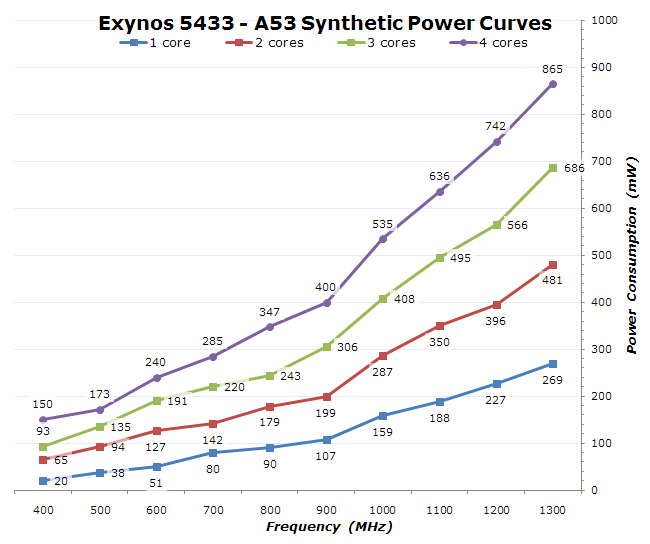
A53-power-curve.png


But I read that A53 doesn't have out of order execution although, it does have a shorter pipeline compared to A57: 8 stages vs 18 stages.
So, a quad core A53 used as LITTLE clocked at 1Ghz would use just over half a Watt at load?

Would that fit into the power/cooling rato with a quad core A57 as big and GPU clocks? Would it explain the fan?
 

LordOfChaos

Member
Has a big.LITTLE configuration been ruled out?

Lots of speculation about what customizations were done, could be that big and LITTLE run concurrently instead of either/or... with little handling OS? That would explain why devs were told they had all four cores to work with.

We only heard the four A57s leak, if the A53s remain in there we haven't heard of them. Not impossible by far of course, but what you're talking about with using both clusters seamlessly is heterogeneous multi-processing, the Tegra X1 only had cluster switching

Cluster switching, lets call it 'gen one' big.little
Big.Little_Cluster_Switching.png


in-kernel switching, which allows a mix of 4 of any cores
In_Kernel_Switcher.jpg


HMP, any and all
Global_Task_Scheduling.jpg
 

Schnozberry

Member
Well, yeah, 10/7nm and A73s and Volta and so forth would be nice, but there's always better technology around the corner. The most important thing for Switch technologically is that they set themselves up in a way that gives them the greatest possible latitude when developing future hardware while retaining compatibility, and they're actually in a good spot for that, with technology like ARMv8 and Vulkan giving them the ability to target a wide variety of performance levels and form-factors (and potentially even CPU/GPU vendors) going forward. Being able to use Maxwell/Pascal, the first desktop-class GPU arch in a long time to use tiled rendering, is also very helpful in that it allows them to do away with their usual route of using a big pool of (expensive) on-die VRAM in favour of a unified single memory pool.

I think they just a little late to the party to hit 16nm. Had Wii U recovered enough to plan for a Holiday 2017 release, then we might be seeing A72 cores and a 16nm GPU that affords them a little more headroom for clocks. The leakage and thermal issues with 20nm are very real, as the Snapdragon 810 showed in 2015, and the Switch is reflecting that now with the limited clock speeds.

I think the Switch is the most forward thinking piece of tech we've seen from Nintendo since the Gamecube. It's just easy to see how timing sort of tied their hands.
 
We only heard the four A57s leak, if the A53s remain in there we haven't heard of them. Not impossible by far of course, but what you're talking about with using both clusters seamlessly is heterogeneous multi-processing, the Tegra X1 only had cluster switching

Cluster switching, lets call it 'gen one' big.little
Big.Little_Cluster_Switching.png


in-kernel switching, which allows a mix of 4 of any cores
In_Kernel_Switcher.jpg


HMP, any and all
Global_Task_Scheduling.jpg

heterogeneous multi-processing would mean they share the load, though? That's not what I'm meaning. Unless it just means sharing memory.


The fact that we haven't heard of them is why I think they'd be used for OS if they are still there. The X1 has a big.LITTLE confiuration so Nintendo would have had to chosen to remove the cores if they aren't there. The leaks are based around what devs have access to. If LITTLE is being walled off for OS/firmware, then devs wouldn't have access to it or even need to know about it.


Those engineering man-years had to go somewhere other than just playing with frequencies on a standard X1.
 

ggx2ac

Member
So, a quad core A53 used as LITTLE clocked at 1Ghz would use just over half a Watt at load?

Would that fit into the power/cooling rato with a quad core A57 as big and GPU clocks? Would it explain the fan?

It doesn't explain anything. All we know is that the dev kits have 4 A57 cores because it's a Jetson TX1.

There's this rumour that is annoying with the dev kits from October being "more powerful" than the ones in July which doesn't tell us much.

It's annoying because the leakers never said what dev kit version belonged to whatever leaks they were making. As soon as Eurogamer leaked the clock speeds it's as though Laura Kate Dale went into damage control by mentioning the October dev-kits are more powerful than the ones in July without even specifying anything.

We can assume the clock speeds increased but we don't know if that's the case and it's weird Laura Kate Dale didn't go into specifics when she has already leaked a lot of things about Nintendo Switch.
 

blu

Wants the largest console games publisher to avoid Nintendo's platforms.
Interesting. That must be their own design then, because AFAIK ARM didn't put out reference designs for the A72 at 20nm. Just 16nm and later 28nm.
True, but MediaTek are among the largest early adopters (along with Huawei) of ARM Holdings' designs. I guess MT just had to ask ARM kind enough for a 20nm A72 port.
 
It doesn't explain anything. All we know is that the dev kits have 4 A57 cores because it's a Jetson TX1.

There's this rumour that is annoying with the dev kits from October being "more powerful" than the ones in July which doesn't tell us much.

It's annoying because the leakers never said what dev kit version belonged to whatever leaks they were making. As soon as Eurogamer leaked the clock speeds it's as though Laura Kate Dale went into damage control by mentioning the October dev-kits are more powerful than the ones in July without even specifying anything.

We can assume the clock speeds increased but we don't know if that's the case and it's weird Laura Kate Dale didn't go into specifics when she has already leaked a lot of things about Nintendo Switch.
Just thinking that if A53s were running concurrently and took the OS load off the A57s it would seem as though the CPU got a bump from the outside.
 

ggx2ac

Member
Has it been confirmed that the NS is 20nm? I'm a little out of the loop for the last couple of days due to work.

Nothing is confirmed and probably nothing more will be leaked until after the Switch presentation assuming Nintendo doesn't go into details about the specs.

Guess we'll be waiting for a Chipworks die shot in March, possibly.
 

MDave

Member
Have you also tried 'userspace' mode?

Hah, not sure what 'performance' mode does then. 'userspace' seems to do the trick of keeping the CPU from dropping down.

Results!

http://puu.sh/tgW36/d066a480ca.jpg
http://puu.sh/tgW5h/372ec0d750.png

GPU thermal throttling is more ... consistent when the CPU clock is more consistent? Hah.

Just wanna throw out how awesome it is you are doing thesw tests.

Thanks, just want to give back to the community! It's also fun, and I think I'm the only one here with a Shield TV, rooted, that allows me to measure the GPU and set the CPU states :p Probably why Eurogamer and such didn't or wouldn't test too deeply, as rooting voids the warranty. I started mainly wanting to test the memory bandwidth to see if really is something Nintendo would want to customise in the chip, but it seems to be quite capable of 1080p with 8x MSAA in my tests, hah.

(Large image warning: 2.52MB)
http://puu.sh/tgWLi/e1a78d4272.png

Ok. If the unit is hot and throttled from the previous test, why is it immediately able to use max speed when starting that test in both cases? My concern here is that the graph doesn't correlate with the explanations I'm reading and either my understanding is wrong or the how we're reading the data is incorrect. It seems to be that the CPU is not listening to your attempts to set its speed, but rather only capping the maximum speed available. During the tests prior to the final physics test, it looks like the CPU is simply using a lower frequency because it can, not because it has too (throttling due to heat)

You're right, for some reason 'performance' CPU governor doesn't do exactly what it says on the tin, but 'userspace' does. Check above results :)
 

LordOfChaos

Member
heterogeneous multi-processing would mean they share the load, though? That's not what I'm meaning. Unless it just means sharing memory.

Having both of them on at the same time can't be done in the previous two implementations, the first of which Tegra X1 uses. See the diagrams, first type is one of two clusters on at once, second type is 4 of 8 of either core type mixed on at once, third type is dynamic scheduling to any and all of 8 cores. This is not regarding load sharing.

Either way, it would need the interconnect to be updated over the TX1, even if you mean having the little cluster wholly separate. That would still mean modifying it to allow them to operate separately. Possible, but no proof for or against to even guess on.
 

Vena

Member
It doesn't explain anything. All we know is that the dev kits have 4 A57 cores because it's a Jetson TX1.

There's this rumour that is annoying with the dev kits from October being "more powerful" than the ones in July which doesn't tell us much.

It's annoying because the leakers never said what dev kit version belonged to whatever leaks they were making. As soon as Eurogamer leaked the clock speeds it's as though Laura Kate Dale went into damage control by mentioning the October dev-kits are more powerful than the ones in July without even specifying anything.

We can assume the clock speeds increased but we don't know if that's the case and it's weird Laura Kate Dale didn't go into specifics when she has already leaked a lot of things about Nintendo Switch.

Ya this is the peskiest rumor with no clarity to it.
 
Having both of them on at the same time can't be done in the previous two implementations, the first of which Tegra X1 uses.

Either way, it would need the interconnect to be updated, even if you mean having the little cluster wholly separate.

Has there been anything leaked that would represent all those man-years of engineering?
 

blu

Wants the largest console games publisher to avoid Nintendo's platforms.
I started mainly wanting to test the memory bandwidth to see if really is something Nintendo would want to customise in the chip, but it seems to be quite capable of 1080p with 8x MSAA in my tests, hah.

(Large image warning: 2.52MB)
http://puu.sh/tgWLi/e1a78d4272.png
Are you working on a game of yours?

Has there been anything leaked that would represent all those man-years of engineering?
Software can be a very laborious endeavour.
 

LordOfChaos

Member
Has there been anything leaked that would represent all those man-years of engineering?

They made a bespoke API, NVN. 500 man years sounds impressive but wouldn't make most chip makers bat an eye, that's 250 people working 2 years. A ground up GPU can take hundreds working 4 years for instance. Particularly including a ground-up API in that mix, I think people should set their expectations to 'closer to standard' than something insanely customized, and at best they'll be pleasantly surprised.
 

EDarkness

Member
They made a bespoke API, NVN. 500 man years sounds impressive but wouldn't make most chip makers bat an eye, that's 250 people working 2 years. A ground up GPU can take hundreds working 4 years for instance.

If they already have a base to start with, then they wouldn't need to start from scratch which cuts down on the number of man-years they'll need. Still if all they did was make a couple of small modifications on the X1, then it doesn't seem all that impressive. I'm hoping that this just isn't the case. Maybe they did something interesting with it and we'll find out a little bit this week.

Nope, but you can bet on that.

Nothing is confirmed and probably nothing more will be leaked until after the Switch presentation assuming Nintendo doesn't go into details about the specs.

Guess we'll be waiting for a Chipworks die shot in March, possibly.

Thanks, guys. Trying to catch up right now.
 

Oregano

Member
So far we've heard no major customization. When the 3DS was announced it was specifically named as a Pica200 in the device and even then DMP created a new Maestro function for the 3DS.

I think they would have just said an X1 if it was a standard X1. There would be no real reason to hide that.
 

MuchoMalo

Banned
The handheld's clockspeed may have been chosen because it was simply 2.5x less than the clock frequency docked, which was itself chosen due to the thermal thottling that the original TX1 did.

I also believe that Nintendo would be careful about how many cores to reserve for the OS. The devs that are working on the system already knows what they can work with, so we would have heard something if it was too much of a compromise.

I mentioned that first part in my post.
 
They made a bespoke API, NVN. 500 man years sounds impressive but wouldn't make most chip makers bat an eye, that's 250 people working 2 years. A ground up GPU can take hundreds working 4 years for instance. Particularly including a ground-up API in that mix, I think people should set their expectations to 'closer to standard' than something insanely customized, and at best they'll be pleasantly surprised.

I actually don't think they did anything to modify the GPU at all based on leaks. The only thing I think they may have done is allow the LITTLE cores to function independently to handle OS. That would make the leak that devs have access to all four A57 cores make sense. They already had a base API to work off of considering Switch was registered to use Vulkan, the would indicate that NVN may be a branch of the existing API tweaked for the specific hardware.
 

LordOfChaos

Member
I actually don't think they did anything to modify the GPU at all based on leaks. The only thing I think they may have done is allow the LITTLE cores to function independently to handle OS. That would make the leak that devs have access to all four A57 cores make sense. They already had a base API to work off of considering Switch was registered to use Vulkan, the would indicate that NVN may be a branch of the existing API tweaked for the specific hardware.

Totally possible, but no proof for or against it as I said. It would be great if it was true and there was no OS reservation on the larger cores.
 
Totally possible, but no proof for or against it as I said. It would be great if it was true and there was no OS reservation on the larger cores.

Honestly, I was hoping asking the question would get a little birdy to drop a crumb regarding Devkit CPU access/usage, lol. Was probably too much to hope for considering NDAs. Or even if the devs would be able to know much other than how their game is running from one devkit to the other.
 

AzaK

Member
The handheld's clockspeed may have been chosen because it was simply 2.5x less than the clock frequency docked, which was itself chosen due to the thermal thottling that the original TX1 did.

I also believe that Nintendo would be careful about how many cores to reserve for the OS. The devs that are working on the system already knows what they can work with, so we would have heard something if it was too much of a compromise.

So are we looking at a docked limit driven by a mobile restriction (Small space) and inability to cool efficiently. That is, if they had have been more aggressive with cooling when docked, would we have something better, even on a stock TX1?
 

antonz

Member
So are we looking at a docked limit driven by a mobile restriction (Small space) and inability to cool efficiently. That is, if they had have been more aggressive with cooling when docked, would we have something better, even on a stock TX1?

The Size of the device plays a large factor. The Switch is roughly 14mm thick. Shield TV is roughly 26mm thick. So you start to see just how compact the Switch is. The Jetson TX1 has when taking those sizes comparatively a massive heatsink that is close to 26mm thick by itself with a fan.

Nintendo Would have needed to basically have the Wii U Gamepad all over again to realistically even begin to push the X1 at max without throttling and even then that may not have been enough.
 

LordOfChaos

Member
What (if any) would be the most likely customizations Nintendo would ask for based on what we know of TX1?

Looking at everything Nintendo has made since the N64, I'm looking forward to learning about memory chain optimization, as they've been paranoid about memory bandwidth limitations since then.
 

ggx2ac

Member
What (if any) would be the most likely customizations Nintendo would ask for based on what we know of TX1?

Don't know about most likely but here's the rundown.

- Add L3 Cache containing 4MB of SRAM similar to iPad Air 2 for some low latency fast memory.
- More CUDA cores for better performance while keeping low clock speeds while making the GPU larger because 20nm nodes suck.
- Upgrade from A57 to A72 CPU cores because they are much better in performance but require a 28nm or 16nmFF node.
- Shrinking the TX1 SoC to 16nmFF to increase clock speeds while keeping down power consumption.

Keep in mind 20nm screwed things up for SoC designs because they leak too much heat at high clock speeds.

A good example of this is a comparison between the A8X SoC and the A9X SoC.

C1xZH5oVIAABjfC.jpg


A8X had 3 CPU cores clocked at 1.5GHz and customised their PowerVR GPU to add 2 more GPU clusters so they could get more performance while keeping the clock speed low. They added 4MB SRAM for L3 Cache. This is all on a 20nm node.

In comparison, A9X has 2 CPU cores clocked at 2.26GHz and 12 GPU clusters powering the iPad Pro which has a huge display resolution. They put in 128-bit LPDDR4 RAM but no L3 Cache although, it's not exactly known why.

It’s also while looking at A9X’s memory subsystem however that we find our second and final curveball for A9X: the L3 cache. Or rather, the lack thereof. For multiple generations now Apple has used an L3 cache on both their phone and tablet SoCs to help feed both the CPU and GPU, as even a fast memory bus can’t keep up with a low latency local cache. Even as recent as A9, Apple included a 4MB victim cache. However for A9X there is no L3 cache; the only caches on the chip are the individual L1 and L2 caches for the CPU and GPU, along with some even smaller amounts for cache for various other functional blocks.

The big question right now is why Apple would do this. Our traditional wisdom here is that the L3 cache was put in place to service both the CPU and GPU, but especially the GPU. Graphics rendering is a memory bandwidth-intensive operation, and as Apple has consistently been well ahead of many of the other ARM SoC designers in GPU performance, they have been running headlong into the performance limitations imposed by narrow mobile memory interfaces. An L3 cache, in turn, would alleviate some of that memory pressure and keep both CPU and GPU performance up.

One explanation may be that Apple deemed the L3 cache no longer necessary with the A9X’s 128-bit LPDDR4 memory bus; that 51.2GB/sec of bandwidth meant that they no longer needed the cache to avoid GPU stalls. However while the use of LPDDR4 may be a factor, Apple’s ratio of bandwidth-to-GPU cores of roughly 4.26GB/sec-to-1 core is identical to A9’s, which does have an L3 cache. With A9X being a larger A9 in so many ways, this alone isn’t the whole story.

What’s especially curious is that the L3 cache on the A9 wasn’t costing Apple much in the way of space. Chipworks puts the size of A9’s 4MB L3 cache block at a puny ~4.5 mm2, which is just 3% the size of A9X. So although there is a cost to adding L3 cache, unless there are issues we can’t see even with a die shot (e.g. routing), Apple didn’t save much by getting rid of the L3 cache.

Our own Andrei Frumusanu suspects that it may be a power matter, and that Apple was using the L3 cache to save on power-expensive memory operations on the A9. With A9X however, it’s a tablet SoC that doesn’t face the same power restrictions, and as a result doesn’t need a power-saving cache. This would be coupled with the fact that with double the GPU cores, there would be a lot more pressure on just a 4MB cache versus the pressure created by A9, which in turn may drive the need for a larger cache and ultimately an even larger die size.

As it stands there’s no one obvious reason, and it’s likely that all 3 factors – die size, LPDDR4, and power needs – all played a part here, with only those within the halls of One Infinite Loop knowing for sure. However I will add that since Apple has removed the L3 cache, the GPU L2 cache must be sizable. Imagination’s tile based deferred rendering technology needs an on-chip cache to hold tiles in to work on, and while they don’t need an entire frame’s worth of cache (which on iPad Pro would be over 21MB), they do need enough cache to hold a single tile. It’s much harder to estimate GPU L2 cache size from a die shot (especially with Apple’s asymmetrical design), but I wouldn’t be surprised of A9X’s GPU L2 cache is greater than A9’s or A8X’s

http://www.anandtech.com/show/9766/the-apple-ipad-pro-review/2

So unless Nintendo planned their SoC with 16nmFF in mind, it may not be much different to the TX1 SoC.
 

Vena

Member
The Size of the device plays a large factor. The Switch is roughly 14mm thick. Shield TV is roughly 26mm thick. So you start to see just how compact the Switch is. The Jetson TX1 has when taking those sizes comparatively a massive heatsink that is close to 26mm thick by itself with a fan.

Nintendo Would have needed to basically have the Wii U Gamepad all over again to realistically even begin to push the X1 at max without throttling and even then that may not have been enough.

I still think the tiny size of the Switch (depth) suggests the node isn't 20nm because, given what we've seen of the Shield throttling, it doesn't seem like even the Shield can reliably handle clocks much higher than what we're seeing of the Switch... and the Sheild TV is in a larger chasis with more room for fan sizes and air to move for thermal conduction concerns.

Given what MDave showed, the Switch isn't very far from "locked" Sheild TV performance in docked, and also has to charge a battery.

But maybe I am off my rocker!
 

GaryD

Member
But if NVIDIA had their stuff running on 16nm why wouldn't they have done it themselves? Seems to me they would have if they could have. Maybe they tried, it went wrong and this was plan b.
 

ggx2ac

Member
But if NVIDIA had their stuff running on 16nm why wouldn't they have done it themselves? Seems to me they would have if they could have. Maybe they tried, it went wrong and this was plan b.

Could you rephrase that because I don't get what you're referring to.
 
But if NVIDIA had their stuff running on 16nm why wouldn't they have done it themselves? Seems to me they would have if they could have. Maybe they tried, it went wrong and this was plan b.

I don't think there was ever a comment on the process size the X1's in the new Shield are made at
 

EDarkness

Member
But if NVIDIA had their stuff running on 16nm why wouldn't they have done it themselves? Seems to me they would have if they could have. Maybe they tried, it went wrong and this was plan b.

Could be any number of reasons. My personal belief is that they didn't see the need to go "all out" on the Shield TV since it probably won't sell as much in the first place. They can save up a big hardware reveal for when the next iteration of Tegra and to see how the NS does in the gaming space.
 

Branduil

Member
What (if any) would be the most likely customizations Nintendo would ask for based on what we know of TX1?
Most people seem to think any customizations would focus on memory bandwidth and how the CPU interacts with the OS. Which would make sense for a system focused on gaming.
 

ggx2ac

Member
I don't think there was ever a comment on the process size the X1's in the new Shield are made at

I'm certain that if the die was shrunk, they would've made a big deal about the Shield TV being more power efficient, instead they talked about software.

The casing of the old Shield TV has a lot of space for the HDD and is probably the reason the newer model without the HDD is small.

The product is releasing next week right? Maybe a tech site will do a teardown of the new models with the HDD and without.
 

Hermii

Member
Is IT possible Nintendo wanted a more powerful 16nm ff but for whatever reason changed it to an x1 in the final 6 months?

We had initial romours about a bleeding edge chip, Natedrake and others heard pascal, the nvidia blog post said same architecture as top performing cards. And we may end up with close to a bog standard tx1 from 2015?
 
Is IT possible Nintendo wanted a more powerful 16nm ff but for whatever reason changed it to an x1 in the final 6 months?

We had initial romours about a bleeding edge chip, Natedrake and others heard pascal, the nvidia blog post said same architecture as top performing cards. And we may end up with close to a bog standard x1 from 2015?
There has been no gossip about any type of downgrade. In fact, LDK latest information about the final dev kits implied that they are even stronger than before despite not changing that much. NateDrake said that there was indeed talks about Pascal chips at some point, but Nintendo/Nvidia could have for some reason decided to keep 20nm and only took certain elements of Pascal instead.

Perhaps it is something that Nintendo wanted to include that was only available in 20nm (like the eDRAM in the Wii U only being available in 45nm), but we just don't know at this time.

Either way, we are definitely not getting a bog standard TX1.
 
Status
Not open for further replies.
Top Bottom