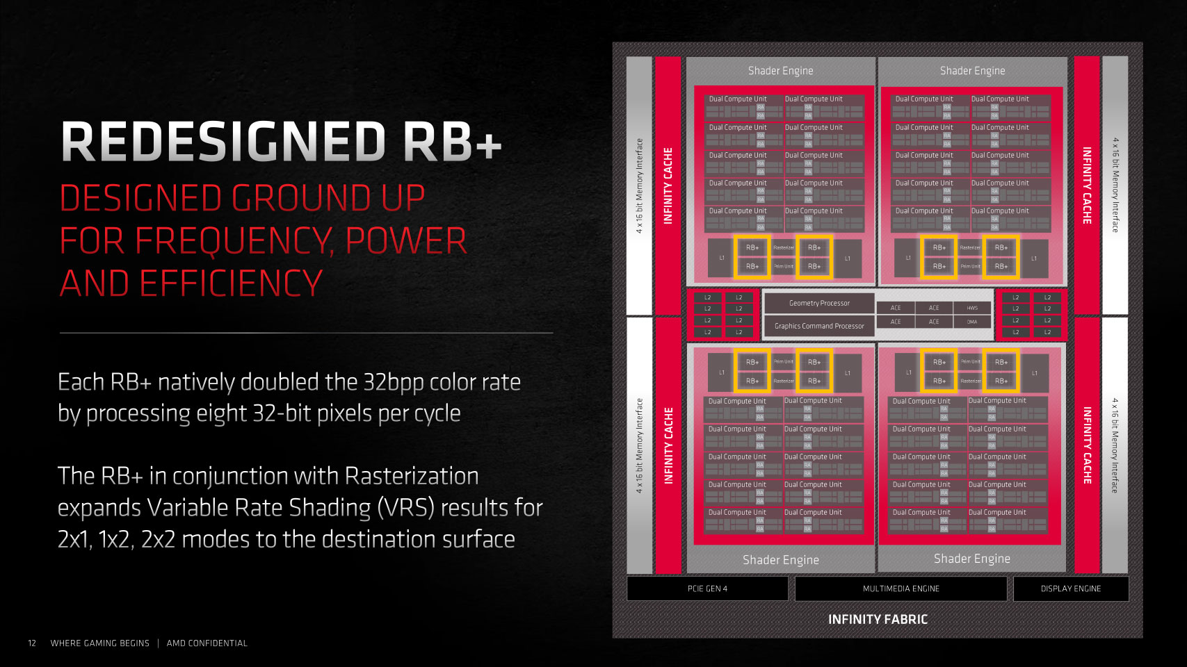
According to the official whitepaper, a shader engine consists of a rasterizer unit and a primitive unit. Series X clearly has a prim unit and raster unit in each of those 4 engines. Are you certain that isn't 4 distinct shader engines?
Could it be 4 SE with 1 SA per SE? Perhaps. Doesn't look that way tho. Idk.
If you look at the slide with their GPU layout, it has 2 things labeled shader input. Those would seem to indicate 2 shader engines, idk.
The 2 groups of 28 CUs are also spaced further apart in 2 groups, which also seems clear that its 4 SA but 2 SE.
And btw, none of this is a criticism of the XSX. Just my thoughts and guesses.
Edit - another thought is ROPs:
Navi 21 die has 80 CUs in 4 Shader Engines, with 128 ROPs. 32 ROPS per SE.
Navi 22 die will have 40 CUs, 2 SEs, with 64 ROPs. 32 ROPs per SE.
PS5 GPU has 40 CUs, 2 SEs, with 64 ROPs. 32 ROPs per SE.
XSX GPU also has 64 ROPs. So .. it likely has 2 SEs and same 32 ROPs per SE.
Otherwise, it would have just 16 ROPs per SE if it had 4 SEs. Personally, I doubt that.
Oh god, that nonsense from Moore's law again. The console has access to all 12 TFLOPS for gaming. There isn't any performance dedicated solely to cloud computing.
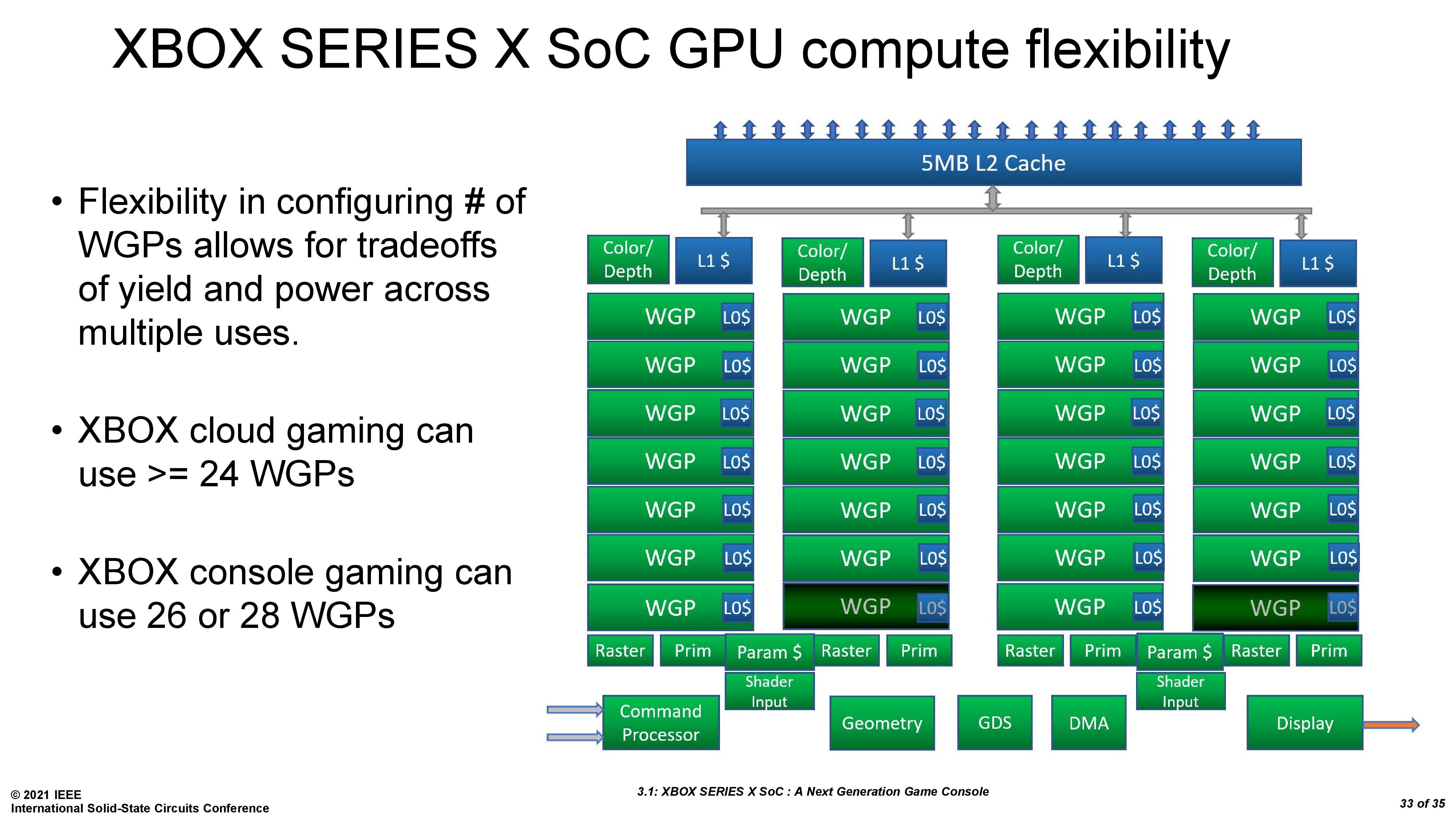
Thats not what that poster meant. I don't know or care what that youtuber guy said but Phil Spencer himself has said the XSX SoC was designed with the Azure silicon engineer team as well. That's why Azure engineers did the hot chips presentation. The chip was built for multiple purposes, console chip and xcloud server chip.
Thats why Xbox have said the XSX when used in xcloud servers can run 4 Xbox One games simultaneously from 1 SoC. Because it was built for that as well. Thats why in their recent presentation they discuss the flexibility of the CU design to serve both console & cloud server roles.
"Multiple uses" refers to use in console (XSX) and cloud (xcloud server.)
Xbox Cloud Gaming refers to when used in cloud servers. They only need 24 DCUs, 48 CUs total. Because Xbox One games use 12 CUs each. Each Xbox One has 7 DCUs on chip, 6 active. Thats why they built the XSX GPU to be 4 arrays of 7 DCUs. To be able to run 4 Xbox One games at once from 1 chip. Xbox One games use 5 GB RAM. For 4 games, the server chip would need 20 GB RAM. For the typical setup of 20 GB RAM, one would use either 10x 2 GB RAM chips or 20x 1 GB RAM chips, connected to a 320 bit interface. Thats most likely why the XSX console has the 320 bit bus but split bandwidth setup with 16 GB RAM. They wanted more bandwidth than 448 GB/s, and wanted the 320 bit bus on die for its secondary use in xcloud, but didn't want to spend the extra cash per console to put 20 GB RAM in each XSX. And using faster 16 Gb/s G6 RAM would have also cost more and or increased heat generated inside the console.
Plus, normally, any XSX chip that doesn't yield 52 CUs would end being wasted. But for using in xcloud, they only need 48, so they can actually save extra money and use more of the chips per wafer that they're paying TSMC to make for them. Its a clever way of building 1 chip that can serve 2 roles.
This is why once they determined they had 52 active CUs in the XSX, they just picked the clock speed to achieve 12 TFLOPS which Phil said was their goal all along. They did the same thing with XOneX, where they arrived at 40 active CUs and set the oddly specific clock of 1.172 GHz needed to get exactly 6.0 TFLOPs. And the same thing with XSS. Its a 20 CU GPU, and their goal was 4 TFLOPs, so they set clock to exactly 1.565 GHz to get exactly 4.0 TFLOPs.