Unknown Soldier
Member
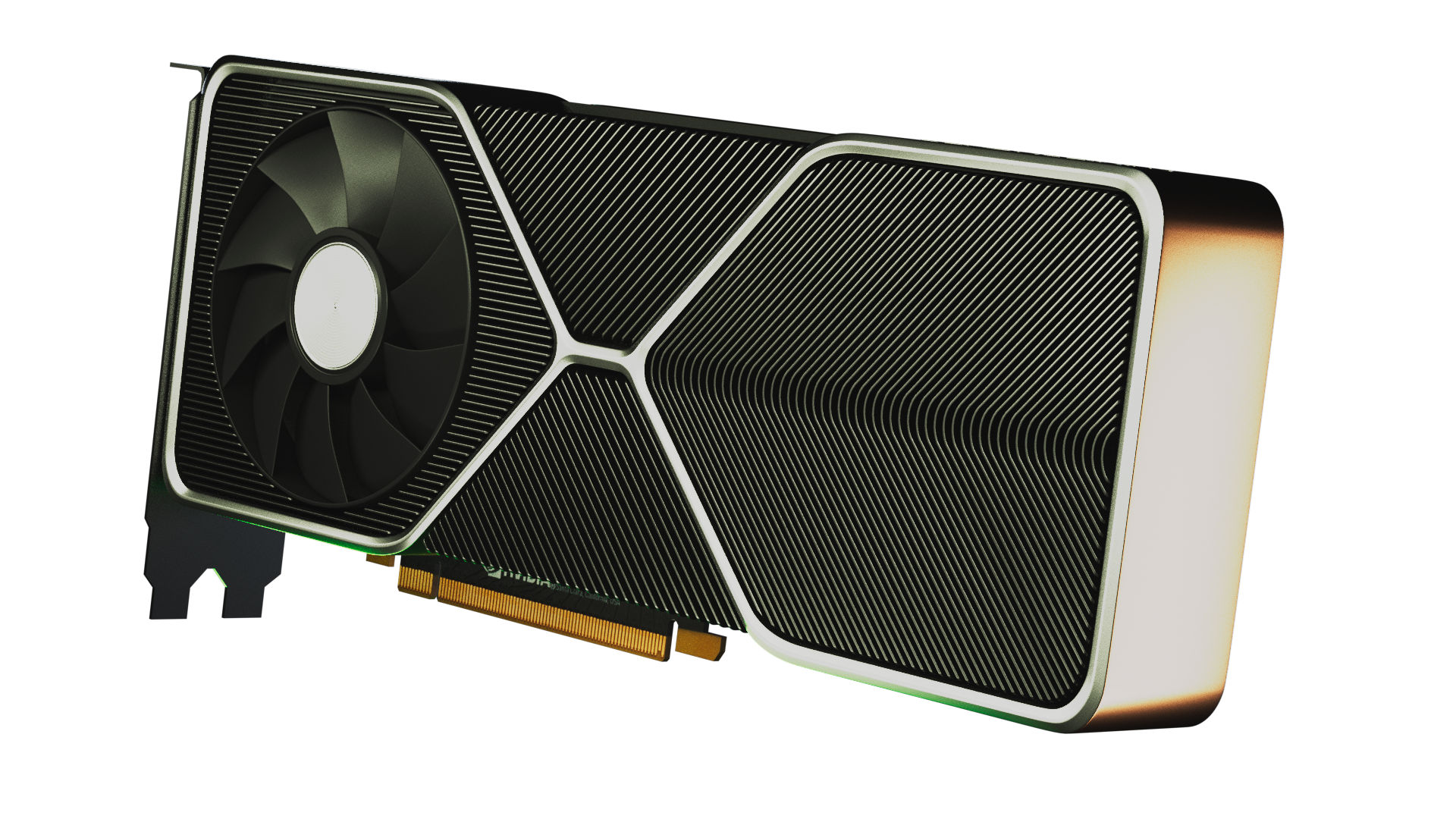
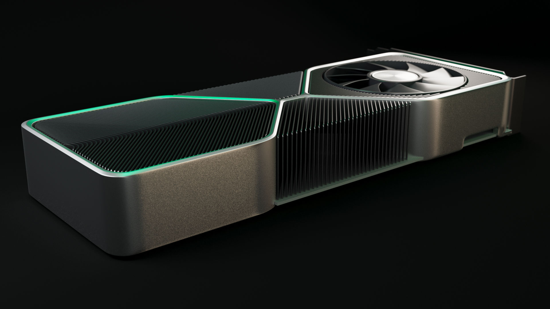
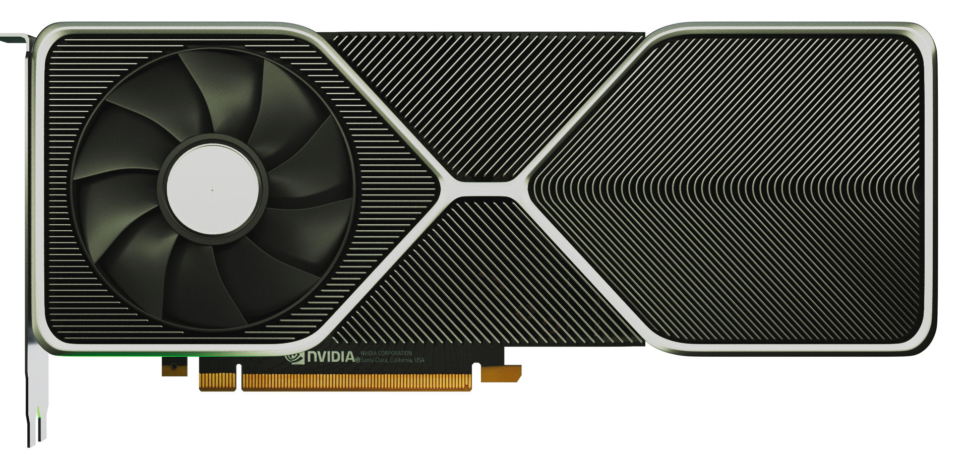
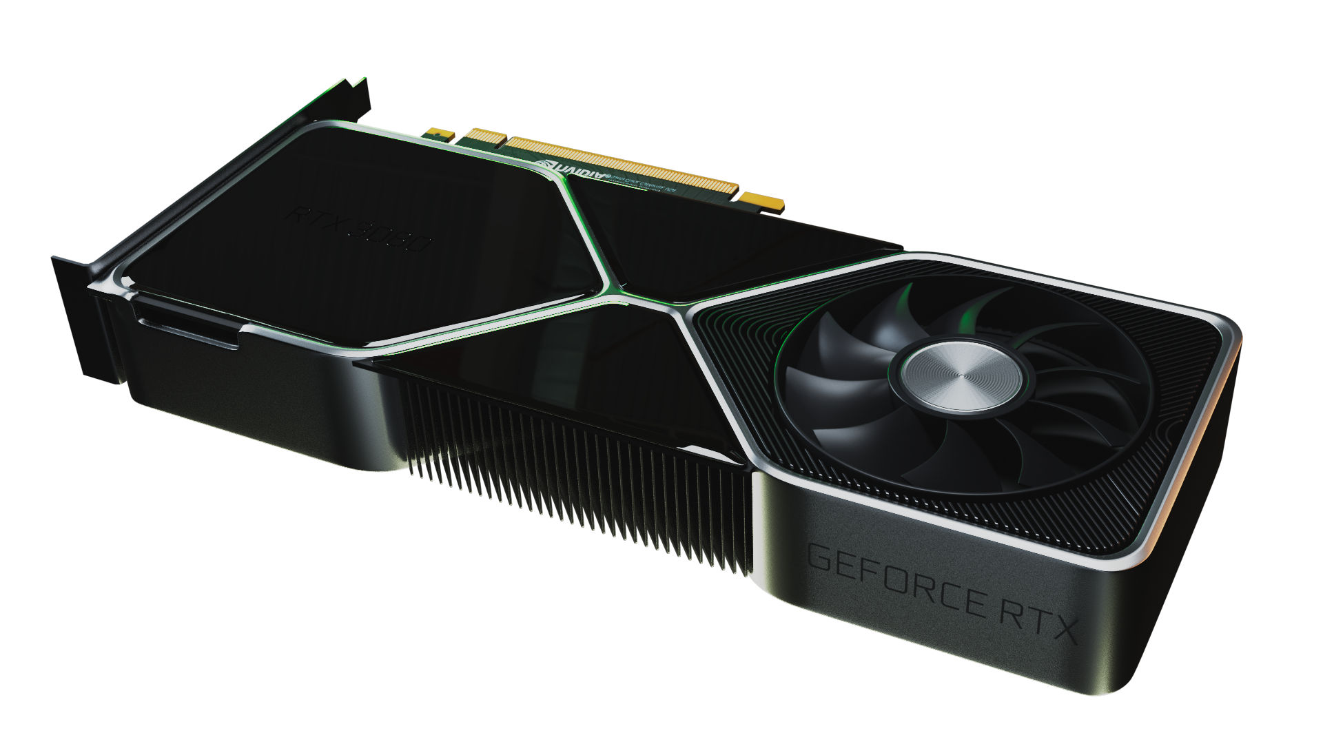
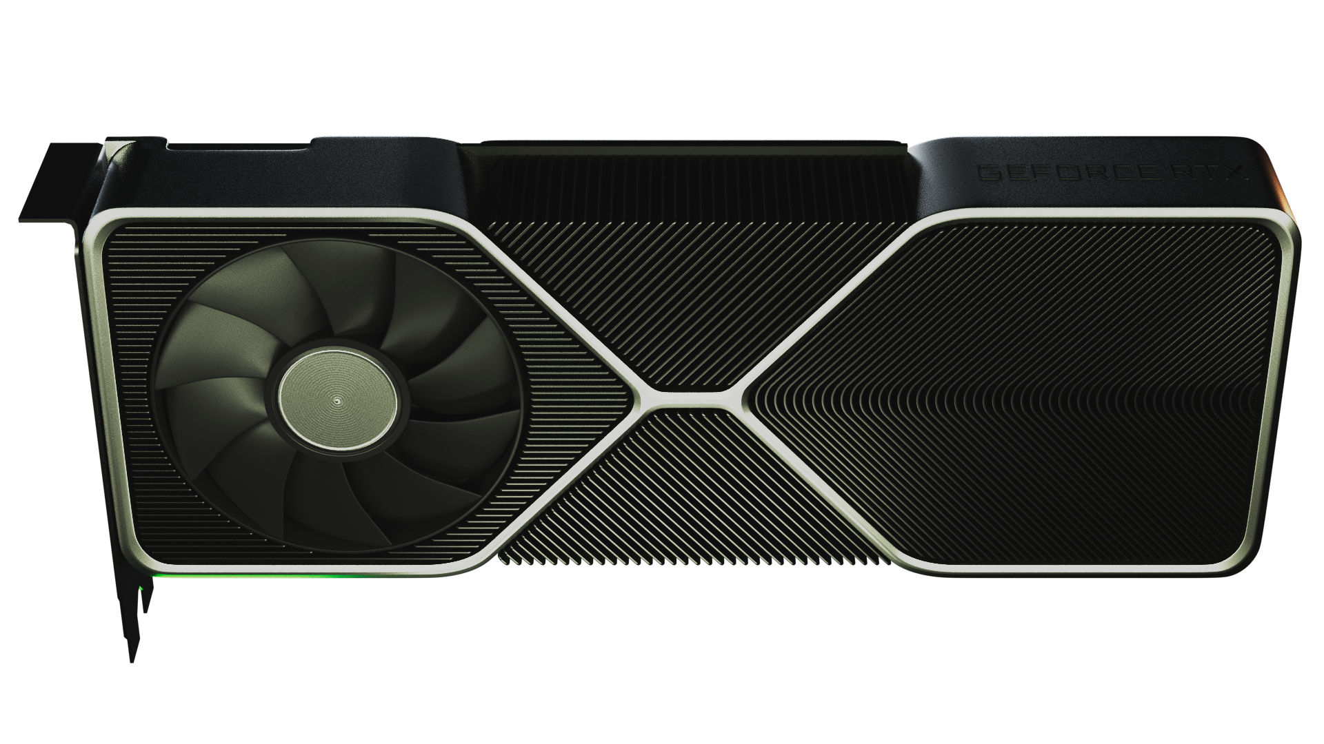
Wait....a fan on both top and bottom? That....doesn't really make any sense. I can't think of any way this benefits cooling. I'm calling fake.
Sounds like you might had bad PSU . You should not need a 1200 watt PSU for 2080 TI 650 wattage is recommend.
You had two options RMA the PSU
Or just buy another PSU with similar wattage.
Trust me if you where overloading the PSU you wouldn't be getting a buzzing sound.
")

Wow, if true Nvidia ain't joking this time. 3080 could be based off the big die, GA102. I hope AMD is prepared for that.
I think AMD will actually try to compete
Note howLeonidas couldn't answer the question about which AMD chip is "RIP"-ed by "leaked" 3080.
AMD is not going after halo product (just yet). 505mm2 is too small for that.
What NV is gonna get is AMD annoying it with cheaper and faster products across broader spectrum, NV would need something substantially larger than 500mm2 for niche cards not challenged by AMD.
RT will be a total misnomer, with only a handful of games supporting it and even then, only for a handful of effects, so expect lots of Leonidast minded sites twist it a lot "AMD is cheaper and faster and (perhaps) consumes less, but that RT thing in NV sponsored games doesn't run that fast". We'll likely see Tesselation Returns: RT edition.
Wait....a fan on both top and bottom? That....doesn't really make any sense. I can't think of any way this benefits cooling. I'm calling fake.
3080 having the same specs as 2080Ti but at 7nm doesn't sound exciting for me, quite the opposite. So either all the improvements will go into Tensor and RT cores, or the rumor is simply false.
Yes. Emphasis on "for them".Big Navi will be a halo product for them.
It won't beat NVs halo, which will be a bigger chip.Whether or not 505mm2 is "too small" for the halo end of the market depends entirely on performance:
Yep. And you chose Vega to compare, because?GP102 was 471mm2 and had 3840 shaders, meanwhile Vega10 was 495mm2 and had 4096 shaders.
Of course its a halo device "for them". Who else would it be a halo device for? They're making it.Yes. Emphasis on "for them".
Remind me when the fastest product you have isn't your halo product.
Or who would expect RDNA2 not to have something much faster than 5700XT.
It won't beat NVs halo, which will be a bigger chip.
Yep. And you chose Vega to compare, because?
That 495mm2 translated into 330mm2 7nm chip, which, even though it was equipped with HBM2 memory, is barely faster than AMD's own Navi 250mm2 chip with cheaper memory.
Have you ever been excited by an x80 GPU?
1080 was quite a jump compared to Maxwell GPUs, not to mention the Ti version. But that was achieved thanks to lower process node, so I expect similar jump this time as well thanks to 7nm. I mean, we already know the specs of the full die.

Fair enough.You don't make this kind of statement when you're not trying compete at the highest end of the market. Whether or not they succeed and "win" they halo end of the market remains to be seen. But it is a halo device.
Just my speculation, based on GA100 being that massive this early into 7nm and how NV was acting in the past.Will it? Do you know the die size for GA102?
1080 wasn't interesting to 980Ti owners with good OCed AIBs.1080 was quite a jump compared to Maxwell GPUs
That depends entirely on how things stack up in terms of performance. AMD could go bigger. In fact in HPC they undoubtedly will. Its a matter of if they think its worth putting the investment in making another massive 600+mm2 die like Fiji. Who knows.Fair enough.
Just my opinion: they'd need to go bananas, way beyond 505mm2 to win "I have the fastest of the obnoxiously priced cards", given how much value does NV see in that.
It could still be touted to "compete at the highest end" with "pay $500 less and get only 15% slower card"
On the Fermi times: as Anand later revealed (don't remember what the article was actually about, sorry), there was a major issue with that node and AMD happened to find brilliant solution to it. That level of discrepancy could happen now only if TSMC is vastly superior to Samsung's process node (as there seem to be no gotchas).
As for why Vega ain't relevant: Vega comes from "starving AMD" times (+Raja).
Perf/transistor wise, Navi is far ahead of it, roughly on par with NV. (so was Polaris, by the way).
Just my speculation, based on GA100 being that massive this early into 7nm and how NV was acting in the past.
GA100 is sold at 20k a piece, 10 per package (mkay, maybe a bit less as two AMD CPUs in that package should cost 10-20k-ish). It is basically "the best you can cram" kind of card.
But what happens to stuff that has only some faulty units? NV doesn't sell a product with them.
1.4Ghz being relatively low: well, with some of the units/non-gaming number crunchers disabled, they surely can go higher.

Tell me about a single case of that sort of nonsense, once Koduri was gone.Whether the designer of the architecture was Raja Koduri, David Wang, or even Lisa Su herself, doesn't matter. At the end of the day, Vega had AMD's logo on it. Its relevant, because they still released the product. They still made big promises. They still made stupid marketing decisions like the inane "Poor Voltage" campaign. Its a product under their brand. Whether it was the product of bad management or bad finances doesn't matter.
Mm, that would be weird, how come it's not on the same node as Navi 20?826mm2 is a huge die. And not only is it huge, its also very dense. It is the same node as Navi 10
I think here, we had "The Leather man has played 'piss partners off' with yet another company" case.Do they waste all of their TSMC 7nm wafers on GA100
And then you get 10k+ per each of those 27. How much is that 300 waffer + process?Most wafers are 300mm diameter. In such a wafer at most you can have 58 GA100 chips per wafer. That's not a lot. TSMC's N7 has a defect rate of around 0.1 per cm2. That's very very good. But even with a defect rate that low, with that huge 826mm2 die you're left with only 27 fully functioning chips per wafer.
GA100 is a (in a way, certainly when compared to CPUs, very dumb) number cruncher, which is likely to be 100% busy, unlike GPUs.Bare in mind, that a cut down GA100 at a relatively low frequency is drawing 400W. Imagine how much power a fully unlocked GA100 would consume - even if you dropped the clocks further, it would be astronomical.
meh
1. One of the shrouds has a small little tiny "NVIDIA" logo, no faker would invest time into putting a small logo on these types of things. It would require pretty specific tooling and usually with fakers they love to put the logo big so that there's no ambiguity to the fake.
2. Irregular PCB shape, both Komachi and Kitty have said this in prior leaks.
3. It says EMC Certification Pending on the PCI-E connector.
4. The design looks familiar to NVIDIA and it's clear NVIDIA loves to change their cooler design every generation, it's definitely unique for a reference card, but too complex for a faker to make themselves, most fakers do something dumb like add three fans based on the existing cooler and call it a day for their "leak".
5. The blue plastic wrap, any faker wouldn't leave this on, they always like the logos to appear unobstructed, also it just seems too legit to have the blue plastic wrap on there.
Sounds like you might had bad PSU . You should not need a 1200 watt PSU for 2080 TI 650 wattage is recommend.
You had two options RMA the PSU
Or just buy another PSU with similar wattage.
Trust me if you where overloading the PSU you wouldn't be getting a buzzing sound.
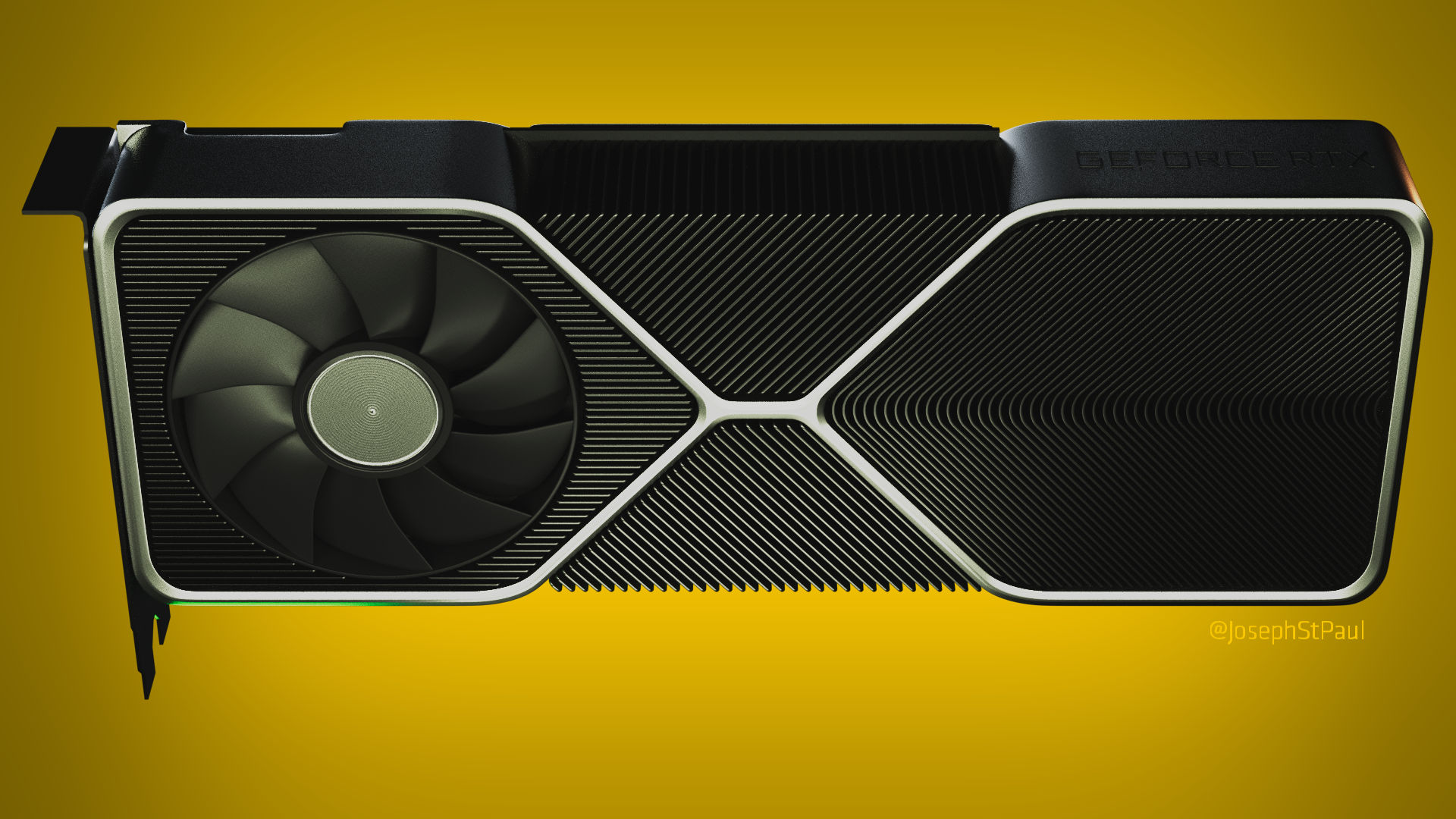
IKR, i don't give a fuck how it looks as long as it stays cool!I genuinely didn't know there was judgement cast on how a gfx card looks, til.
Then why jump to conclusions that 3080 possibly having the same core count as 2080 Ti as being a bad thing? The only possible spec in that tweet where you jumped to your conclusions was core counts.
An x80 GPU has never had higher core counts than the previous gen x80 Ti.
But there was a clock gain in return with each new generation, Pascals could go as high as 2,1GHz compared to 1,4-1,5 on Maxwells, that's why there was such a jump in performance, and when switching from Pascals to Turings the jump was basically non-existent, because the clocks can go higher only by 25-50MHz at best, so if both the core count and clock speeds will remain the same in Ampere GPUs again then sorry, I cannot get excited. Bare in mind once next-gen only games will start to show up, games not made with PS4/XB1 in mind, the requirements will go through the roof if we want to maintain 60FPS and more. Some rumors suggest the RT performance will quadruple, with even better DLSS on top of that, others suggest up to 30TF GPUs, too many different/opposite rumors are out there to make a concrete conclusion if you ask me, I'm personally hoping for all around improvements, in rasterization, RT, DLSS, Mesh Shading, and maybe even some new fancy tech NV will come up with.
 videocardz.com
But there was a clock gain in return with each new generation, Pascals could go as high as 2,1GHz compared to 1,4-1,5 on Maxwells, that's why there was such a jump in performance
and when switching from Pascals to Turings the jump was basically non-existent, because the clocks can go higher only by 25-50MHz at best, so if both the core count and clock speeds will remain the same in Ampere GPUs again then sorry, I cannot get excited.
if you ask me, I'm personally hoping for all around improvements, in rasterization, RT, DLSS, Mesh Shading...
A good design improves cooling. That's the point.You are really salty about that, aren't you? I wonder when a PC will be able to have an SSD IO subsystem as fast as the PS5's. A year, two maybe? On topic, I don't really get the point of an elaborate GPU design, they all kind of look the same and go inside your PC case anyway.
A good design improves cooling. That's the point.
Lots of people have tempered glass cases and can see inside their PC. A backplate looks better. Not complicated.I don't mean the cooling system, I mean the backplate, with the green paint, angular design and whatnot. Some of them even have RGB if I recall correctly. The whole "xtreeem!!" aesthetics just looks to be made for children.
Lots of people have tempered glass cases and can see inside their PC. A backplate looks better. Not complicated.
The backplate is part of the cooling system. A good cooling system seals up the air so that the airflow follows the desired path.I don't mean the cooling system, I mean the backplate, with the green paint, angular design and whatnot. Some of them even have RGB if I recall correctly. The whole "xtreeem!!" aesthetics just looks to be made for children.
You realise your opinion isn't fact, either, right?Better is debatable, RGB looks ridiculous. Still looks like made for children.
Honestly, with a 1080ti, you're set for years to come.150 bucks for a cooler, watch that card cost 1200 bucks. then the ti version double that.
Good luck with that, will sail on my 1080ti until the 4000 hits then.
The backplate is part of the cooling system. A good cooling system seals up the air so that the airflow follows the desired path.
The RGB stuff isn't for "children", it's not to your taste but some people have cases with clear sides that show the components and want the parts to match their visual theme.
It's childish to actually say it's for children. "It's not like i want, it's for children waah waah waah"