The reference to gigabyte 3D stacked wafers being tested attached to quad core CPUs was from 2008. IBM 3D stacking is going on line in 2012 ramping up to full production in 2013 and one of the first products is the logic layer for the 3D stacked memory from Micron and Samsung. The Global Foundries "process optimized building blocks" and custom SOCs is going on-line in 2012 with ramp up to full production in 2013.
Global Foundries/AMD + IBM TSV 3D stacking going on line at the same time MIGHT indicate something but what?
http://chipdesignmag.com/lpd/blog/2011/10/06/samsung-micron-unveil-3d-stacked-memory-and-logic/ said:
What becomes particularly interesting with 3D memory is the possibility of using the memory much more judiciously with heterogeneous cores so only the resources that are needed are actually used. That can save on power while also reserving enough performance for those applications that require more memory and processing power. These memories can be used both in 3D stacks, as well as 2.5D stacked configurations where the memory is connected through an interposer layer.
Both Graham and Pablo Temprano, director of DRAM and graphics marketing at Samsung Semiconductor, acknowledged there are numerous possible scenarios for using this technology. They noted that some customers also are looking at using 3D stacked memory to replace some of the cache on a chip because moving data in and out of memory can be extremely fast.
http://www.infoneedle.com/posting/100175?snc=20641
(A.6) Wide I/O DRAM
Recently, the Hybrid Memory Cube (HMC) Consortium which includes companies like Micron, Intel, Altera, Samsung, Open Silicon, Xilinx, and IBM created an entirely new technology (
http://www.micron.com/innovations/hmc.html). The end results could be a high bandwidth (15x more than DDR3), low power (70% less energy per bit than DDR3), and small form-factor (90% less space than RDIMMS) product as shown schematically in Figure 2a and is planned for fabricated with one of IBMs via-middle TSV technologies shown in Figure 2b [1]. The cross-section is shown in Figure 2c and the logic/memory interface (LMI) is following the new JEDEC Wide I/O SDR (JESD229) standard (
http://www.jedec.org/), which is shown in Figure 2d.
Normally a chip or SOC design is a 2+year effort and there is no way a new memory with new standard could be used without a large lead time. It's now possible to reduce time to market (From AMD) using process optimized STANDARDized building blocks in a SOC. That's half the story, as seen in the picture a SOC substrate with TSVs or bumps must be designed and manufactured. IBM probably has software to design and build a Substrate for a SOC using "Building blocks" built to known standards with little lead time.
The Hybrid Memory Cube appears to be a serial standard like SATA for Hard disks. As such it is probably not practical inside a SOC but the HMC without the logic layer is made up of stacked ultrawide I/O memory wafers built to a standard that might be used for other applications.
PDF on Hybrid memory cube confirms a serial interface with the maximum transfer speed of 1Tb/sec only possible with a optical buss.
http://www.edn.com/article/521730-Microsoft_joins_Micron_memory_cube_effort.php said:
Micron says it will deliver early next year 2 and 4 Gbyte versions of the Cube providing aggregate bi-directional bandwidth of up to 160 Gbytes/second.
Separately, the Jedec standards group is working on a follow on to the 12.8 Gbit/second Wide I/O interface that targets mobile applications processors. The so-called HB-DRAM or HBM effort is said to target a 120-128 Gbyte/second interface and is led by the Jedec JC-42 committee including representatives from Hynix and other companies.
Micron is making 2 gig and 4 gig stacks of ultrawide I/O memory and IBM is making the logic layer, it's not known at this time who is assembling the HMC. The 2 gig and 4 gig Micron memory stacks without the logic layer could be used for other purposes and IBM has the TSV connection template for the Micron memory because they make the logic layer.
Micron Stockholder meeting August 2011:
Graphics and consumer. Fair to say, a little bit of a slowdown here, specifically in the DTV segment. I'll speak more about what's happening in game consoles as well. A pretty good push for more memory coming up in the Game Console segment as a level of redesigns. We'll start to hit it over the next couple of years.
And talking about consumer again here. I thought it'd be beneficial to show you across a couple of key applications how this looks in terms of megabyte per system. On the left, what we have are game consoles. This is a space that's been pretty flat for a number of years in terms of the average shipped density per system. That's going to be changing here pretty quickly. I think everyone realizes that these systems are somewhat clumpy in their development. The next generation of system is under development now and that because of 3D and some of the bandwidth requirements, drives the megabyte per console up fairly quickly. So we're anticipating some good growth here.
We've worked with a number of these vendors specifically on both custom and semi-custom solutions in that space.
I hear that "target Specs" for the PS4 is for GDDR5 memory:
http://www.brightsideofnews.com/news/2011/11/30/radeon-hd-7000-revealed-amd-to-mix-gcn-with-vliw4--vliw5-architectures.aspx said:
A rumor recently exploded that HD 7900 Series will come with Rambus XDR2 memory. Given the fact that AMD has a memory development team and the company being the driving force behind creation of GDDR3, GDDR4 and GDDR5 memory standards - we were unsure of the rumors.
Bear in mind that going Rambus is not an easy decision, as a lot of engineers inside AMD flat out refuse to even consider the idea of using Rambus products due to company's litigious behavior. However, our sources are telling us that AMD is frustrated that the DRAM industry didn't made good on the very large investment on AMD's part, creating two GDDR5 memory standards: Single Ended (S.E. GDDR5) and Differential GDDR5. Thus, the company applied pressure to the memory industry in bridging GDDR5 and the future memory standard with XDR2 memory. The production Tahiti part will utilize GDDR5 memory, though.
Is AMD going to continue investing in future memory standards? We would say yes, but with all the changes that have happened, it just might take the executive route to utilize available market technologies rather than spending time and money on future iterations of GDDR memory. After all, AMD recently reshuffled their memory design task force. In any case, Differential GDDR5 comes at very interesting bandwidth figures and those figures are something AMD wants to utilize "as soon as possible".
Product list of Hynix
GDDR5
2Gb x32/x16 7.0Gbps Game console, Desktop, Notebook, Workstation, HPC
1Gb x32/x16 6.0Gbps
So game console(s) are going to use GDDR5 (which one and how much). Developer platforms using existing NON-SOC hardware have 2 64 bit DDR3 interfaces for the Fusion ALU and if they are using a faster more efficient 2nd GPU could use GDDR5 for it. All I/O and memory transfer between second GPU and ALU is through the PCIe buss, they don't have a common memory buss. This is a PC design not a game console.
The final design SOC could have the second GPU migrate into the SOC and then it wouldn't use GDDR5 memory but some faster than DDR3 main memory which should be 3D stacked memory, there is no faster than DDR3 until later this year when DDR4 is released (Slower than GDDR5). But guys with access to developers are stating that documentation states the target memory is 2 gig GDDR5 which does not make sense with current designs unless the second GPU and SOC share the same GDDR5 memory buss rather than using the PCIe buss like PCs do. That's a significant design change.
Using key words in the AMD cite above (GDDR5 Differential) brings up a
2011 PDF from Hynix memory
3 Options after GDDR5
GDDR5 Single-ended I/O
- Max. 8Gbps with same power
GDDR5 Differential I/O
- Max. 14Gbps with much more power
HBM*(Wide I/O with TSV) High Bandwidth Memory HBM migrating to mainstream 2-3 years after High-end segmentation
- Lower speed with many I/Os and low power => Handheld low power DRAM
 Upgradable DRAM Speed ==> using higher power faster DRAM at higher clock speed, not for handheld
 Increasable # of I/O
 Flexible # of stack
Graphics Card, HPC, Workstation
Interim Solution between DDR3 and HBM
GDDR5M
 Speed : Max. 4.0Gbps @1.35V
 IO : x16/x8
Based on the strong partnership with AMD, Hynix navigates the best Graphics solutions of each system for the future today.
"Differential GDDR5 comes at very interesting bandwidth figures and those figures are something AMD wants to utilize "as soon as possible". "the company applied pressure to the memory industry in bridging GDDR5 and the future memory standard with XDR2 memory" GDDR5 + some of the XDR2 memory features = differential GDDR5.
It's possible that the final design could have second GPU and SOC share the same GDDR5 differential memory buss rather than using the PCIe buss like PCs do. That's a significant design change from developer platforms and not mentioned in any roadmaps. Differential "XDR" buss GDDR5 would be needed just as the PS3 needed XDR1 because of the speed and length of buss lines outside the GPU and SOC. This would allow efficiencies for the CPU to prefetch for the second GPU as well as a common memory for Zero copy.
Still think the SOC should have a 100 meg or so of Ultrawide I/O memory, may or may not be 3D stacked. Best long term cheapest solution is to have second GPU in the SOC with 2 gigs of 3D stacked ultrawide I/O memory which appears to be on the roadmap and as mentioned before, timing puts it as a possible for 2014. Developers were told target spec is GDDR5 which with something like a Differential buss or wider than normal data buss can increase memory bandwidth. Also with custom packaging mentioned above, a reduction in the number of chips that have to be attached to the motherboard can reduce the drive voltage and current.
Tradeoffs for differential buss memory is a more expensive motherboard (more traces) and memory with higher power but memory buss driver in SOC and GPU would be driving a lower voltage and should run cooler.
AMD has access to wide I/O DRAM interface
EDIT:
It appears that it's possible to have 2 gigs of wide I/O inside the SOC now but 4 gigs would have to wait and/or be more expensive. The following needs to be understood completely, quad channel DDR3 or 4 "don't think about it" needs to be understood, it's not gong to be in a future design for the same reason the PS3 Cell @ 40nm can't be easily scaled to 32nm, the XDR interface is too large just like 4 DDR channels in a AMD Fusion would be. The next node process shrink would have issues and that should be part of Sony and Microsoft long range plans.
A custom memory interface is an absolute MUST!
http://www.amdzone.com/phpbb3/viewtopic.php?f=532&t=139005&start=50#p218132 said:
DDR4 is not much faster than DDR3 ... it all depends on latencies (tymings). Also DDR4 tends to consume more relative power for the higher "speeds" ... better would be AMD to launch a LR (load reduced) non-registered non-ECC high speed standard!... just a crazy idea!... but since AMD is now in the DRAM business also, it could make better with what is already there.
About a quad channel APU, just DON'T think about it... DRAM DIMM interfaces are absolutely HUGE and scale terribly bad with smaller process nodes ... the necessary lane layout would mean a much larger chip than necessary, perhaps curtailing the possibility of ULV 17W bins. Also it defeats the purpose for mobile, entry to mainstream desktop markets...
The better way to deal with the memory bandwidth problem of APUs is to have TSV eDRAM... IBM could help in the design ( i think AMD already has a license for the macro designs) and also the Wide I/O DRAM interface of which consortium AMD is part, all fits like a charm.
So after Kavery we can have an APU with 512 to 1GB of TSV DRAM on the package, no POPs no interposers, cooling solutions already exist, so the "execution" parts don't have to lose much (if anything).
heck! it can have also an interposed on package like Haswell will have 512MB to 1GB of DRAM
Heck this is nothing new, quite before any Haswell, only it could be way much better... and instead of a Radeon it will be an APU on that package... and by the time it will be necessary it can have 2 DRAM chips instead of 4, cause TSV is starting to be big among DRAM IDMs, and those chips can have up to 8 stacked dies (4Gbit/die each means 4GB/chip or 8 GB for total of 2 DRAM chips on package -> meaning 1 to 2GB total will be relative inexpensive... heck! 4 DRAM dies + 1 controller (a LR type ) and it will be 2GB in one single chip (with up to 128bit interface on the Wide I/O standard)... for the GPGPU on the APU!..
Micron stated in a stockholder meeting that they are providing custom and semi-custom memory for next generation game consoles.
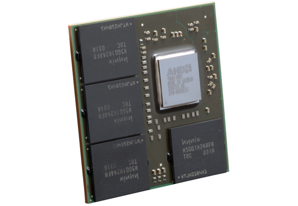
2 Gig of stacked RAM in the SOC (one to two layers high only, more and fill/heat issues crop up) would be an efficient and cost effective design. More memory at this time would have to be outside the SOC (probably a Load Reduced DDR3 128 bit wide custom package) but could be attached to a package like in the above picture. These are the kinds of design changes that can take place, the SOC is probably locked at this point.
In this picture on the bottom right is a prototype SOC with 2 memory chips inside the SOC (two rectangles on the right).
So either way, inside the SOC or outside on the package is possible. Trace length is not an issue with either method but the number of pins, how wide the Memory buss (I/O) is an issue. Inside the SOC you could have a 512 bit buss, outside the SOC on the package 256 or 128 bit buss.
Only if there is going to be a second GPU outside the SOC would GDDR5 memory be used. DDR3 memory as a second pool for the GPU is not going to happen if it's a HSA design. Rumors of split pool and odd memory sizes are probably from developer platforms which can only approximate a final design using current hardware made for PCs.
Over and over I see Memory wall issues mentioned (memory bandwidth has not kept up with CPU needs) and APU Fusion SOCs needing large memory bandwidth, Game consoles will push against the memory wall even harder.
This is the point of the SimiAccurate post on the PS4, "Stacked memory and lots of it". Stacked memory uses TSVs to stack like on like memory to increase the density which decreases the total trace length on motherboards. This is necessary to have faster memory and also reduces motherboard costs. Game console volumes justify/make practical a custom memory for a game console. The interface between SOC to memory outside the SOC is another "Game console volume justifies/makes economically practical" the cost of a custom interface.
Just to be clear about custom memory interface; current DDR memory controllers are 64 bit wide and to create a 256 bit buss you use 4 DDR memory controllers. A custom DDR memory controller connected to custom memory might be ONE 256 bit DDR memory controller connected to between 1 and 4 external Stacked memory chips that would be replaced in the next refresh with a HMC "Copper"multi-serial interface or an optical (1Tbye/sec) interface. Game consoles don't need expandable memory so the most cost effective design is to include the memory inside the SOC with a 256 or 512 bit interface. If this is not possible this generation then a 256 bit external interface allows for an easy refresh to support 256 bit memory inside the SOC in 2 years.