-
Hey, guest user. Hope you're enjoying NeoGAF! Have you considered registering for an account? Come join us and add your take to the daily discourse.
You are using an out of date browser. It may not display this or other websites correctly.
You should upgrade or use an alternative browser.
You should upgrade or use an alternative browser.
- Status
- Not open for further replies.


vpance
Member
Maybe it just wasn't worth leaking?
Ovech-King
Gold Member
There is no way Sony settles for anything less than base native 4k graphics for the ps5 . How do you look in 2025 if so ? Doesn't make sense that why I'm thinking they are going all in at easy 4k 60 fps performance
Last edited:
Insane Metal
Member
Arthur Gies... wrong? OH NO IT CAN'T BE
Fake
Member
Impossible. After all this time?
Last edited:
CyberPanda
Banned
Microsoft Project Denali a Game Changer for Flash Storage at Scale
Microsoft Project Denali is a potential game-changer for flash storage at the scale Azure operates at. The company outlined how and why this is moving into production this year at OCP Summit 2018
 www.servethehome.com
Microsoft presented its new infrastructure developments at OCP Summit 2018. Last year, the buzz was around Project Olympus which was successful and deployed in Azure. This year, Microsoft’s contributions are focused on security and storage. We wanted to highlight Microsoft Project Denali for flash storage which may have major repercussions in the storage industry.
Microsoft Project Denali Background
Starting out the background information, Microsoft threw out some numbers. 30% of global flash output consumed by enterprise and cloud. Of that 30%, half is consumed by big cloud companies or roughly 15% of global output. Of that amount, Microsoft consumes “multi-exabytes” of flash storage each year. The message behind this is that Microsoft and other hyper-scalers are huge consumers of NAND flash and that it is a technology that makes up a large portion of the Azure infrastructure.
Since it is a large part of the Azure infrastructure, Microsoft sees challenges with the current generations of SSDs. Most of these challenges boil down to the fact that SSDs are designed as a tight product between the NAND, controller, and firmware rather than being seen as raw storage to a larger software-defined paradigm.
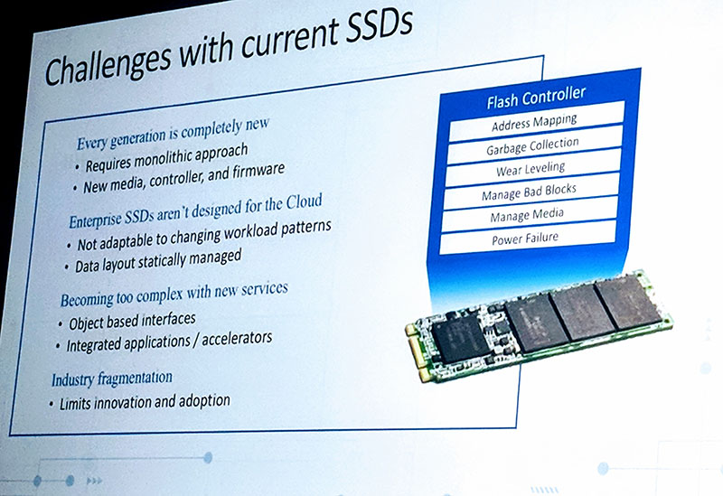
Microsoft Project Denali Challenges With Current SSDs In Azure
Microsoft acknowledged that every SSD supplier is driving innovation, but not necessarily in the same way. Project Denali is designed for cloud-first storage. Microsoft wants to be able to take advantage of new NAND and storage class memory as it becomes available. As such, it needs to disaggregate the current storage model and use software-defined data placement that works in tight coordination with the SSD.
Project Denali has focused on four main goals:
(Source: Microsoft Azure)
- Flexible architecture for innovation agility: Workload-specific optimizations, FTL managed as cloud services component
- Rapid enablement of new NAND generations: NAND follows Moore’s Law; SSDs: hours to precondition, hundreds of workloads
- Support a broad set of applications on massively shared devices: Azure (>600 services), Bing, Exchange, O365, others; up to hundreds of users per drive
- Scale requires multi-vendor support & supply chain diversity: Azure operates in 38 regions globally, more than any other cloud provider
Microsoft Project Denali Disaggregates Flash Model
Microsoft Project Denali is designed for the disaggregation of flash storage. Instead of all of the address mapping, garbage collection, and wear leveling happening on the SSD itself, Microsoft thinks that its Azure cloud workloads would be better serviced by managing the data placement at a higher level.
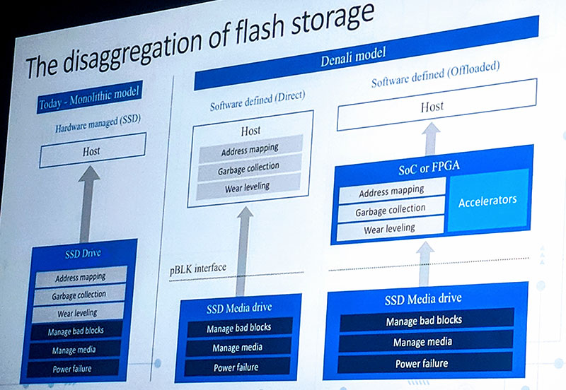
Microsoft Project Denali For Azure The Disaggregation Of Flash Storage
In this new paradigm, SSDs would still be responsible for the raw media layer, taking care of ECC and bad blocks. The new job of SSDs will simply be to present “perfect NAND” to the software layers above. Perfect NAND can be simplified is an array of NAND at a certain latency.
Microsoft thinks software can define address mapping, garbage collection, wear leveling. This is because it believes the application knows the workload pattern the best and can decide how to lay out the data on the device. Making applications or higher-level software aware means that software can be used to lower write amplification, lower costs, and better performance by exposing parallelism. Using this model, SoCs or FPGAs can be used to accelerate the storage tasks across broader arrays of NAND.
To the SSD vendors, this should sound terrifying. Many of the functions that these vendors use to differentiate essentially move up the software stack. If an SSD or NAND provider needs to only ensure that it is presenting NAND that is functional and will retain data, then it lowers the intelligence and value SSD vendors can deliver. Microsoft knows this and if you were looking to push cost out of a large deployment, this is one way you can do it.
Project Denali Prototypes to m.2 Deployment
This is a project that has been ongoing for years. Microsoft, Dell, Micron, Samsung, Seagate and others all have investments in a company, CNEX Labs that has been the primary developer of the new storage class. Over the years, it has provided a few different prototypes of what these devices can look like.
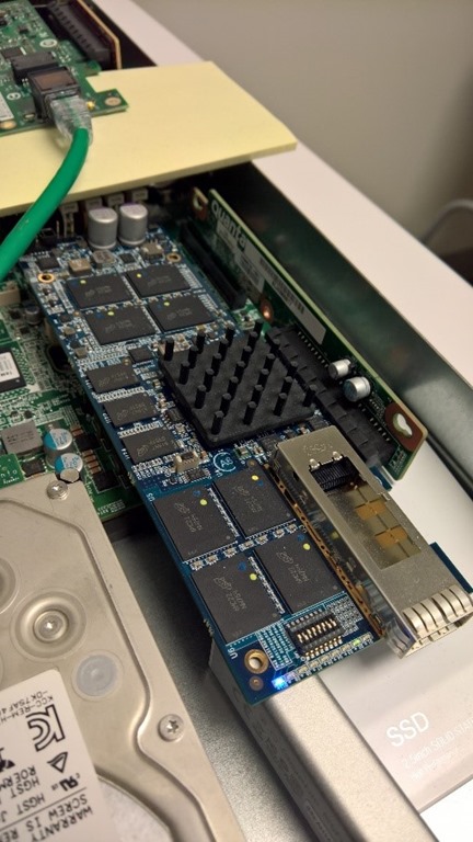
Microsoft Project Denali Prototype
On stage at OCP Summit 2018, we got our first glimpse of the first m.2 drive in the hand of CNEX Labs co-founder Alan Armstrong.
Microsoft Project Denali Prototype M.2
Those in attendance were told that this new m.2 form factor will be deployed in data centers this year. As you can see, the form factor has been miniaturized and better productized. Also, with deployment only months in the future, Project Denali is moving from the theoretical prototype space to something in use by potentially millions of customers in the next few quarters.
Other Perspectives on Project Denali
There are many implications of this technology, especially in the ecosystem. On stage, the companies were able to list a number of prominent partners for the project.
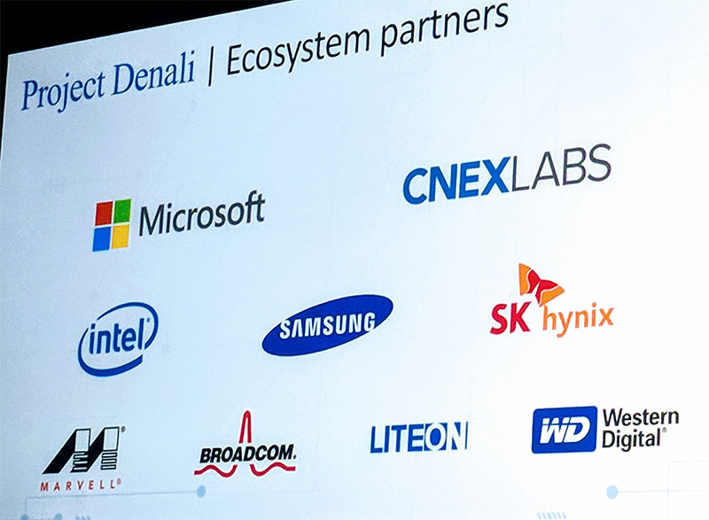
Microsoft Project Denali Ecosystem Partners
At the show, we asked several of the vendors what they thought of this. There was some concern over how much IP the NAND makers would have to share to make this work. Likewise, Microsoft is such a large flash buyer that this was seen as something that may end up being fact on that account.
While editing this article, we were able to speak to Robert Hormuth, CTO, VP/Fellow, Server & Infrastructure Systems at Dell EMC. His 30-second take is that this is certainly an interesting technology, but it is not quite ready for enterprise customers in its current form. He also said that Dell EMC is keeping an eye on the technology as it matures and will continue to evaluate it going forward.
We asked other hyper-scalers who were at the conference and they said they are interested to see what else comes from the project.
Final Words
We do not see this as taking over the consumer market or the lower-end enterprise market anytime soon. If you are dealing with a small number of devices and fewer users/ applications, the current model is both well understood and works well. Instead, we see this as a cost and performance push by the hyper-scale players as it leads to the commoditization of hardware. At the same time, for a large hyper-scaler like Microsoft that has CPU and FPGA fabrics widely deployed, Project Denali makes sense as a next-step solution for lowering costs and extracting value from a massive scale.
Aceofspades
Banned
The PS5 price will be decisive to win the next generation and stay in the lead
PS5 WILL sell better than Xbox no matter what the price. PlayStation brand is simply way bigger and has massive worldwide appeal.
Evilms
Banned
PS5 WILL sell better than Xbox no matter what the price. PlayStation brand is simply way bigger and has massive worldwide appeal.
I'm not so sure, as proof the $599 PS3 had trouble getting started unlike the PS1, PS2 and PS4 which have from the beginning asphyxiated the competition, as the price remains an important factor and I I'm sure Sony are aware of that.
ResilientBanana
Member
This will most likely be the case. But again, Microsoft is more interested in selling GaaS than consoles. It’s more lucrative.Agree.
PS5 can lose US to Nextbox but worldwide it will always sell better and launching near each other PS5 will never be behind.
CyberPanda
Banned
Just like Jack Tretton said, they are going in great into the new generation, but competition is going to be extra tough this time around. Especially with new contenders entering the ring. It’s going to be a very interesting generation.Agree.
PS5 can lose US to Nextbox but worldwide it will always sell better and launching near each other PS5 will never be behind.
pawel86ck
Banned
Quake 4 was unoptimized launch title, but without any doubts Xbox 360 GPU was comparable to high end GPU's back then, in fact it was first GPU with unified shaders. I remember one year before xbox 360 launch 2x Geforce 6800 ultra were used to run Unreal Engine 3 tech demo, yet xbox 360 run it on single GPU. Xbox 360 GPU was even faster than PS3 GPU that launched one year later (although CELL was helping GPU as well).2005 we have these graphic cards:
GeForce 7800 GTX (Jun 2005)
Radeon X1800 XL (Sep 2005)
Radeon X1900 (Jan 2006)
At that time the GPU power was not mensured with FLOPs... so there is no direct comparison.
But at time the Xenos was inferior in games to these GPUs.... it is just more advanced in terms of design.
Quake 4 never run at the same framerate/resultion than PC with these cards.
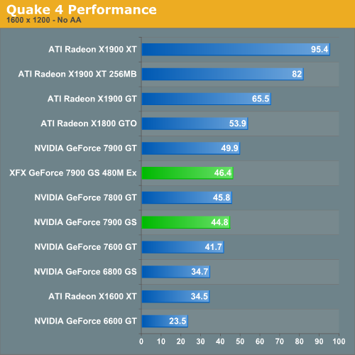
On Xbox 360 it runs at 1280x720 (no AA) unlocked 60fps (dips to 30fps).
Last edited:
ethomaz
Banned
I don’t disagree 360’s was more advanced.Quake 4 was unoptimized launch title, but without any doubts Xbox 360 GPU was comparable to high end GPU's back then, in fact it was first GPU with unified shaders. I remember one year before xbox 360 launch 2x Geforce 6800 ultra were used to run Unreal Engine 3 tech demo, yet xbox 360 run it on single GPU. Xbox 360 GPU was even faster than PS3 GPU that launched one year later (although CELL was helping GPU as well).
But high-end PC at same time delivered better graphics (resolution and framerate) even being less advanced (old tech).
You can find benchmarks for any game between PC and 360 with the high-end cards launched before 360 and all games will run on PC with better resolution, framerate and AA.
Last edited:
CyberPanda
Banned
I agree, but that Xenos card was state of the art. Especially in regards to unified shaders.I don’t disagree 360’s was more advanced.
But high-end PC at same time delivered better graphics (resolution and framerate) even being less advanced (old tech).
ethomaz
Banned
It was based in the incoming new architecture (R600)... maybe it was the last time AMD surprised nVidia after they brought ATI... it took few years to nVidia delivery unified shaders at same level.I agree, but that Xenos card was state of the art. Especially in regards to unified shaders.
CyberPanda
Banned
Yep. ATI was amazing back in the day.It was based in the incoming new architecture (R600)... maybe it was the last time AMD surprised nVidia after they brought ATI... it took few years to nVidia delivery unified shaders at same level.
DragoonKain
Neighbours from Hell
I’m excited about fast load times and stuff, but for me I’m not a geek when it comes to that stuff, I just care about the quality of the library of titles. For the PS5 I’m most interested in the OS and features. Is it easy to navigate? Easy to transfer saves and data and stuff? Customization other than themes would be nice.
And please for the PS5 controller, I love the dual shock 4, but get rid of that fucking light thing on the top. Its novelty is fucking useless anymore
And please for the PS5 controller, I love the dual shock 4, but get rid of that fucking light thing on the top. Its novelty is fucking useless anymore
Last edited:
CyberPanda
Banned
You will get the light again and enjoy it.I’m excited about fast load times and stuff, but for me I’m not a geek when it comes to that stuff, I just care about the quality of the library of titles. For the PS5 I’m most interested in the OS and features. Is it easy to navigate? Easy to transfer saves and data and stuff? Customization other than themes would be nice.
And please for the PS5 controller, I love the dual shock 4, but get rid of that fucking light thing on the top. It’s novelty is fucking useless anymore

Tarkus98
Member
Please be “enlightened “.I’m excited about fast load times and stuff, but for me I’m not a geek when it comes to that stuff, I just care about the quality of the library of titles. For the PS5 I’m most interested in the OS and features. Is it easy to navigate? Easy to transfer saves and data and stuff? Customization other than themes would be nice.
And please for the PS5 controller, I love the dual shock 4, but get rid of that fucking light thing on the top. It’s novelty is fucking useless anymore
devilNprada
Member
Yup, but things are different now. I am mostly bantering a bit and not completely serious, because obviously I have no idea what Sony and MS aim for.
And also we are still more than 1 year away from next gen console and things can change.
I am just being very conservative with my expectations because I don't think that pushing really hard is worth it, especially considering how bad AMD hardware scales when being pushed high. The thermals and power draw SKYROCKETS and I just don't see Sony buying super expensive top of the line 7nm chips to put into a mass market console.
So basically it comes also down to how good Navi really is, how high it clocks, what the thermals and power draw are and if it is possible to easily cool that in a console form factor.
For me it is all about the other things that the PS5 (and Navi aswell atleast the rumors) offers at this point. I am not that worried about raw TFLOPs, because it doesn't really mean that much. A good Navi architecture with 8TF would make me much more happy than hot and power hungry Vega with 12TF. (as long as Navi is architecturally superior to Vega that is)
Yes that is something I have been thinking about aswell.
Sony is in a perfect position. They definitely have money to "invest" into the Playstation and brand and I think they shouldn't try to make a super cheap console to manufacture but rather a high build quality console, with good components and take a small loss on it.
They will make much more from PSN and services and all that digital stuff anyways. (and of course physical game sales with the 30% cut they take).
Sony should leverage their lead and extend it.
As to how much RAM is the sweet spot I really can't say. I feel like between 2012 and 2017 the RAM usage EXPLODED and all those 2GB cards and 4GB PCs are basically useless nowadays.
But I have no idea if Sony can get away with 16GB for games or if they need 20/24. Impossible to say.
In general of course I always "hope" for more, but I know that the perfect console will never exist and there will always be better hardware and in the end Sony and the devs have to deal with what they got and they will make all our jaws drop either way.
I think that many websites will hail the PS5 if it comes in at 12TF as an absolute beast and monster and that mindset will jump onto the mass market customers.
Especially the comparison between PS5 and XboxNext will be "important". So I guess many customers will be confronted with it around the release time and what leads up to.
But I don't think that it matters much. Unless Sony screws up the PS5 will outsell the XboxNext even if it is like 40% slower, because of brand loyalty, Japan and Europe.
It also looks like Sony is doing exactly (atleast what I think) is right with the PS5. Backwards Compatability, ultra fast SSD, better hardware and now the only 2 remaining checkmarks imho are great AAA games and pricepoint.
Even most people that know what TF are and know roughly how they translate to gaming performance don't even know what that would actually mean (me included. For me there are just kind of a very vague performance number that is only really good for comparing GPUs with the same architecture)
In the end it will be for the devs to decide what they do with the resources they have at hand. I think the PS5 will be a very harmonic system with no real "obvious" bottlenecks, but rather a console that is pretty balance. I expect to see more options in games including FoV and fps/graphics settings like we have seen a couple of games trying to do 30fps better graphics/60fps worse graphics (or lower resolution).
I mean I guess it could be $399, but it certainly sounds like Mark Cerny wants us to expect a higher price point.
499$ sounds like the exact spot they will land on given what Shawn Layden said about the PS3 price and how that was a big mistake.
Considering inflation, cost of labor etc. then $499 in 2020 is not that much of a price increase over $399 in 2013. Maybe like $70 or so, but I think $499 is still fine for a console even though, like I said earlier in this thread, I think the $399 route + taking a loss and selling more consoles for a bigger consumer installbase is the better way to go.
Agree completely.. and with the backwards compatability and now cross play (or at least the intent to have) being confirmed; they should provide a premium product because the adoption rate will be slow regardless.
I believe the graphics in games like rdr2 are so good at this point, people aren't going to rush out to get either a 399 or 599 ps5 for marginally better graphics. Now, no load times on the other hand; is a completely different incentive.
DemonCleaner
Member
Let's do a better explanation (I guess).
That is the actual CU in GCN up to version 5.1 (or 1.5.1):
* maybe the cache changed between versions but the numbers of units never changed until now.
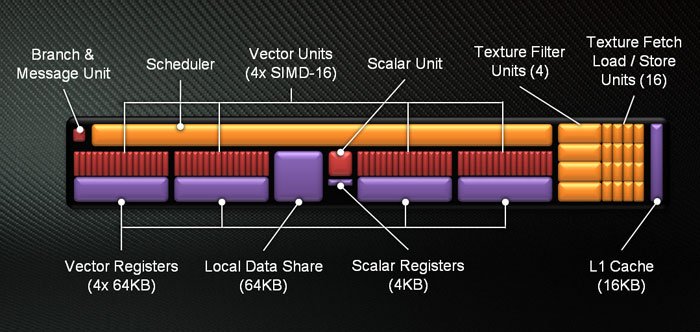
What that means?
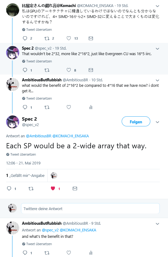
That means a CU in GCN has 4x SIMD-16 lanes per CU, or in easy terms, GCN has 4 goups of 16SPs in each CU.
To use these SPs you need to schedule waves of 16 processing instructions of the same type (the data can be different but the instruction needs to be the same).
That way the minimum you run in a CU is 16SPs per time and the max 64SPs per time but they needs to be in waves of 16SPs... trying to make it easy you need 64 same processing instructions send in 4 waves to fullfill a CU... if your code was not optimized for that then it will use 1, 2 or 3 waves instead of 4.
That generate inefficiency because you have a CU with 64SPs but most of time it is using 16, 32 or 48SPs only.
You need to optimize the code to take advantage and runs most of time with 64SPs at full work in a CU.
In simple terms, actual CGN schedule tasks in waves of 16SPs in a CU.
The worst case scenario a CU will use only 16SPs... best case scenario the CU will use 64SPs... there is the middle always in waves of 16 so 32 and 48 SPs being used.
What changes in the GCN 6.0 (or 1.6.0)?
The SIMD-16 wave is changed to SIMD-32 wave... that way you need 32SPs of the same type instruction being schedule in waves for a CU... the CU will always run with 32CUs or at max 64SPs... there is no middle and the wave is the minimum 32SPs.
That means more efficiency?
In terms... the change make the minimum your CU can be using is 32SPs instead of 16SPs in the past that indeed means the CU will be always at least being used at half-power while before it could be used at 1/4 of it power... that means less SPs per SP in idle (not doing anything).
But here is maybe the big issue... it is easier to group SPs in waves of 16 instead 32.
If you can't group 16 (old) or 32 (new) same type of processing instruction to make a wave then you will even to use only one SP send a wave of 16/32 that makes the power consumption increase in the new way because you will have always running a wave with 32SPs even when you need to use only one SP... before you needed only a wave of 16SPs running to use one SP.
So if the Scheduler is not smart (the magic needs to be here) to group waves of 32 instructions the perf/watt will decrease, the efficiency will decrease because it is easier to group waves of 16 than 32.
So you have two sides:
1) It become more efficient because it will always be using at least half of 64SPs in a CU.
2) It become less efficient if the Scheduler can't group waves of 32 instructions.
The biggest change that nobody is talking is how the Scheduler will do that magic to make the new GCN design more efficient.
Of course there is side advantages too like the increase in Render Output units.
You are still limited to 64CUs but the limit for others units increased:
4 to 8 SEs
64 to 128 ROPs
well you stumble upon the logical fault in that yourself once or twice in your text. you don't gain efficiency by reducing grainularity from 16 to 32. to enforce that at least 32 lanes are used concurrently, they could have simply introduced a compiler error if data isn't set up correctly. so that can't be the reason they are doing this. please read my twitter excursion on that:
in the meantime i've done some rigorous research (asking dumb questions)
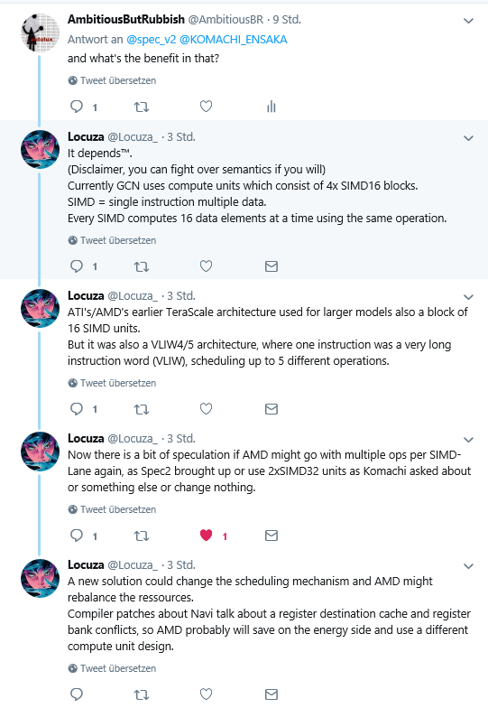
so it looks like the benefit of the new SIMD design is that you can do two different operations concurrently per SIMD
not sure if i got these guys right, but i think it's somewhat like this:
back in times of AMD's Very Long Instruction Word design you could do up to 5 diffrent operations concurrently. that came at the price of a wide data structure which didn't use ALUs well. thats why nvidia and later amd steered away to a one op at a time approach.
however there are dependencies between different tasks and beeing limited to a single opp per cycle will necessary lead to stalls. with the new design once again two operations can be run concurrently. SIMDs won't have to wait a cycle till the correct datatype is ready for further processing. there are not often dependencies of more than two operations at a time. so you can reduce your data width to two instead of 5-wide arrays like with VLIW. the best of both worlds.
this must have taken some serious scheduler and compiler redesign. which might explain the engineer headaches we were hearing about.
Last edited:
DemonCleaner
Member
Launch PS4 was 348mm2 and xbone over 350mm2
i think i said that before but 300mm wafer prices have over doubled since ps4 launch days.
Im confused, is the limit 40CUs or 64CUs?
64 at least. might even be 128 now (if the limited was indeed a SE limit till now). but i wouldn't count on seeing any GPUs with a amount bigger than that anytime soon or ever. this would also lead to a geometry bottleneck once again.
Last edited:
Imtjnotu
Member
Dude for the last time change your Damn font colori think i said that before but 300mm wafer prices have over doubled since ps4 launch days.
64 at least. might even be 128 now (if the limited was indeed a SE limit till now). but i wouldn't count on seeing any GPUs with a amount bigger than that anytime soon or ever. this would also lead to a geometry bottleneck once again.
Last edited:
CyberPanda
Banned
I like how one text is white and the other is grey. LolDude for the last time change your Damn font color
PocoJoe
Banned
IndeedAgree.
PS5 can lose US to Nextbox but worldwide it will always sell better and launching near each other PS5 will never be behind.
Americans probably dont know that while xbox vs. Sony is kind of a battle in the US, rest of the world is like
Adult mma fighter(sony) vs. Disabled kid(xbox) = no chance to win and only few support the kid
JLMC469
Banned
Indeed
Americans probably dont know that while xbox vs. Sony is kind of a battle in the US, rest of the world is like
Adult mma fighter(sony) vs. Disabled kid(xbox) = no chance to win and only few support the kid
Do they care?
ResilientBanana
Member
I’m pretty invested in both sides And would prefer they be evenly matched. But even still games are money, not consoles.Indeed
Americans probably dont know that while xbox vs. Sony is kind of a battle in the US, rest of the world is like
Adult mma fighter(sony) vs. Disabled kid(xbox) = no chance to win and only few support the kid
Last edited:
Alcaze
Neo Member
I'm pretty damn excited to see what both companies pull off, especially because I highly doubt MS will have another Mattrick style unveiling so the start of this upcoming generation might end up being one of the best ever. Hopefully, anyhow.
Then again, I hope the PS5 will still look amazing on my 1080p screen
Then again, I hope the PS5 will still look amazing on my 1080p screen
SonGoku
Member
Increased slightly at 7nm due to it being a new process, nowhere near double.i think i said that before but 300mm wafer prices have over doubled since ps4 launch days.
Yeah i expect 60 to 56CUs depending on yields64 at least. might even be 128 now (if the limited was indeed a SE limit till now). but i wouldn't count on seeing any GPUs with a amount bigger than that anytime soon or ever. this would also lead to a geometry bottleneck once again.
SonGoku
Member
Was that still the case for mid to late gen games?You can find benchmarks for any game between PC and 360 with the high-end cards launched before 360 and all games will run on PC with better resolution, framerate and AA.
Years? The 8800GTX launched 1 year after the 360it took few years to nVidia delivery unified shaders at same level.
CrustyBritches
Gold Member
Yeah,
 DemonCleaner
, you should really stick with the standard font color for those of us on the DarkGAF. You make good posts, but it's difficult to read.
DemonCleaner
, you should really stick with the standard font color for those of us on the DarkGAF. You make good posts, but it's difficult to read.
---
A lot of tech sites picked up the story about the Sapphire rep. I'm really curious about CU count and power consumption. I wonder if it will be like 390/390X or X1X where it's 40CU/44CU. It's gonna be fun to see how AdoredTV's charts pan out in comparison what the rep was saying.
---
A lot of tech sites picked up the story about the Sapphire rep. I'm really curious about CU count and power consumption. I wonder if it will be like 390/390X or X1X where it's 40CU/44CU. It's gonna be fun to see how AdoredTV's charts pan out in comparison what the rep was saying.
LordOfChaos
Member
It was based in the incoming new architecture (R600)... maybe it was the last time AMD surprised nVidia after they brought ATI... it took few years to nVidia delivery unified shaders at same level.
The buyout must have messed with their schedules or something though, for being the ones to ship advanced unified shaders a year earlier than Nvidia, the Radeon 2900 was later than the Geforce 8800 by half a year and wasn't even as good.
Xenos was like X1800 XL execution power but with unified shaders that meant no penalty from when game ratios didn't match fixed shader ratios, so it probably did perform more like a higher end chip. Plus the unique ROPs in eDRAM situation.
Quake 4 was unoptimized launch title, but without any doubts Xbox 360 GPU was comparable to high end GPU's back then, in fact it was first GPU with unified shaders. I remember one year before xbox 360 launch 2x Geforce 6800 ultra were used to run Unreal Engine 3 tech demo, yet xbox 360 run it on single GPU. Xbox 360 GPU was even faster than PS3 GPU that launched one year later (although CELL was helping GPU as well).
I still wonder what the what-if machine universe would look like if Cell had been paired with a good GPU rather than a rush job. Something matching the Xenos, so at the end of the cycle when devs were using Cell well, it wasn't just to fill in for RSX being subpar. But I guess that's the same as asking "what if one console had every technical lead" in any generation.
Last edited:
ethomaz
Banned
Probably something like what happened with PS4 and XB1.I still wonder what the what-if machine universe would look like if Cell had been paired with a good GPU rather than a rush job. Something matching the Xenos, so at the end of the cycle when devs were using Cell well, it wasn't just to fill in for RSX being subpar. But I guess that's the same as asking "what if one console had every technical lead" in any generation.
SonGoku
Member
Post made by
G
gofreak
I've found online about a Sony patent for SSD
TL;DR
- some hardware changes vs the typical inside the SSD (SRAM for housekeeping and data buffering instead of DRAM)
- some extra hardware and accelerators in the system for handling file IO tasks independent of the main CPU
- at the OS layer, a second file system customized for these changes
all primarily aimed at higher read performance and removing potential bottlenecks for data that is written less often than it is read, like data installed from a game disc or download.
This will be one for people interested in some potentially more technical speculation. I posted in the next-gen speculation thread, but was encouraged to spin it off into its own thread.
I did some patent diving to see if I could dig up any likely candidates for what Sony's SSD solution might be.
I found several Japanese SIE patents from Saito Hideyuki along with a single (combined?) US application that appear to be relevant.
The patents were filed across 2015 and 2016.
Caveat: This is an illustrative embodiment in a patent application. i.e. Maybe parts of it will make it into a product, maybe all of it, maybe none of it. Approach it speculatively.
That said, it perhaps gives an idea of what Sony has been researching. And does seem in line with what Cerny talked about in terms of customisations across the stack to optimise performance.
http://www.freepatentsonline.com/y2017/0097897.html
There's quite a lot going on, but to try and break it down:
It talks about the limitations of simply using a SSD 'as is' in a games system, and a set of hardware and software stack changes to improve performance.
Basically, 'as is', an OS uses a virtual file system, designed to virtualise a host of different I/O devices with different characteristics. Various tasks of this file system typically run on the CPU - e.g. traversing file metadata, data tamper checks, data decryption, data decompression. This processing, and interruptions on the CPU, can become a bottleneck to data transfer rates from an SSD, particularly in certain contexts e.g. opening a large number of small files.
At a lower level, SSDs typically employ a data block size aimed at generic use. They distribute blocks of data around the NAND memory to distribute wear. In order to find a file, the memory controller in the SSD has to translate a request to the physical addresses of the data blocks using a look-up table. In a regular SSD, the typical data block size might require a look-up table 1GB in size for a 1TB SSD. A SSD might typically use DRAM to cache that lookup table - so the memory controller consults DRAM before being able to retrieve the data. The patent describes this as another potential bottleneck.
Here are the hardware changes the patent proposes vs a 'typical' SSD system:
- SRAM instead of DRAM inside the SSD for lower latency and higher throughput access between the flash memory controller and the address lookup data. The patent proposes using a coarser granularity of data access for data that is written once, and not re-written - e.g. game install data. This larger block size can allow for address lookup tables as small as 32KB, instead of 1GB. Data read by the memory controller can also be buffered in SRAM for ECC checks instead of DRAM (because of changes made further up the stack, described later). The patent also notes that by ditching DRAM, reduced complexity and cost may be possible, and cost will scale better with larger SSDs that would otherwise need e.g. 2GB of DRAM for 2TB of storage, and so on.
- The SSD's read unit is 'expanded and unified' for efficient read operations.
- A secondary CPU, a DMAC, and a hardware accelerator for decoding, tamper checking and decompression.
- The main CPU, the secondary CPU, the system memory controller and the IO bus are connected by a coherent bus. The patent notes that the secondary CPU can be different in instruction set etc. from the main CPU, as long as they use the same page size and are connected by a coherent bus.
- The hardware accelerator and the IO controller are connected to the IO bus.
An illustrative diagram of the system:
At a software level, the system adds a new file system, the 'File Archive API', designed primarily for write-once data like game installs. Unlike a more generic virtual file system, it's optimised for NAND data access. It sits at the interface between the application and the NAND drivers, and the hardware accelerator drivers.
The secondary CPU handles a priority on access to the SSD. When read requests are made through the File Archive API, all other read and write requests can be prohibited to maximise read throughput.
When a read request is made by the main CPU, it sends it to the secondary CPU, which splits the request into a larger number of small data accesses. It does this for two reasons - to maximise parallel use of the NAND devices and channels (the 'expanded read unit'), and to make blocks small enough to be buffered and checked inside the SSD SRAM. The metadata the secondary CPU needs to traverse is much simpler (and thus faster to process) than under a typical virtual file system.
The NAND memory controller can be flexible about what granularity of data it uses - for data requests send through the File Archive API, it uses granularities that allow the address lookup table to be stored entirely in SRAM for minimal bottlenecking. Other granularities can be used for data that needs to be rewritten more often - user save data for example. In these cases, the SRAM partially caches the lookup tables.
When the SSD has checked its retrieved data, it's sent from SSD SRAM to kernel memory in the system RAM. The hardware accelerator then uses a DMAC to read that data, do its processing, and then write it back to user memory in system RAM. The coordination of this happens with signals between the components, and not involving the main CPU. The main CPU is then finally signalled when data is ready, but is uninvolved until that point.
A diagram illustrating data flow:
Interestingly, for a patent, it describes in some detail the processing targets required of these various components in order to meet certain data transfer rates - what you would need in terms of timings from each of the secondary CPU, the memory controller and the hardware accelerator in order for them not to be a bottleneck on the NAND data speeds:
Though I wouldn't read too much into this, in most examples it talks about what you would need to support a end-to-end transfer rate of 10GB/s.
The patent is also silent on what exactly the IO bus would be - that obviously be a key bottleneck itself on transfer rates out of the NAND devices. Until we know what that is, it's hard to know what the upper end on the transfer rates could be, but it seems a host of customisations are possible to try to maximise whatever that bus will support.
Once again, this is one described embodiment. Not necessarily what the PS5 solution will look exactly like. But it is an idea of what Sony's been researching in how to customise a SSD and software stack for faster read throughput for installed game data.
I did some patent diving to see if I could dig up any likely candidates for what Sony's SSD solution might be.
I found several Japanese SIE patents from Saito Hideyuki along with a single (combined?) US application that appear to be relevant.
The patents were filed across 2015 and 2016.
Caveat: This is an illustrative embodiment in a patent application. i.e. Maybe parts of it will make it into a product, maybe all of it, maybe none of it. Approach it speculatively.
That said, it perhaps gives an idea of what Sony has been researching. And does seem in line with what Cerny talked about in terms of customisations across the stack to optimise performance.
http://www.freepatentsonline.com/y2017/0097897.html
There's quite a lot going on, but to try and break it down:
It talks about the limitations of simply using a SSD 'as is' in a games system, and a set of hardware and software stack changes to improve performance.
Basically, 'as is', an OS uses a virtual file system, designed to virtualise a host of different I/O devices with different characteristics. Various tasks of this file system typically run on the CPU - e.g. traversing file metadata, data tamper checks, data decryption, data decompression. This processing, and interruptions on the CPU, can become a bottleneck to data transfer rates from an SSD, particularly in certain contexts e.g. opening a large number of small files.
At a lower level, SSDs typically employ a data block size aimed at generic use. They distribute blocks of data around the NAND memory to distribute wear. In order to find a file, the memory controller in the SSD has to translate a request to the physical addresses of the data blocks using a look-up table. In a regular SSD, the typical data block size might require a look-up table 1GB in size for a 1TB SSD. A SSD might typically use DRAM to cache that lookup table - so the memory controller consults DRAM before being able to retrieve the data. The patent describes this as another potential bottleneck.
Here are the hardware changes the patent proposes vs a 'typical' SSD system:
- SRAM instead of DRAM inside the SSD for lower latency and higher throughput access between the flash memory controller and the address lookup data. The patent proposes using a coarser granularity of data access for data that is written once, and not re-written - e.g. game install data. This larger block size can allow for address lookup tables as small as 32KB, instead of 1GB. Data read by the memory controller can also be buffered in SRAM for ECC checks instead of DRAM (because of changes made further up the stack, described later). The patent also notes that by ditching DRAM, reduced complexity and cost may be possible, and cost will scale better with larger SSDs that would otherwise need e.g. 2GB of DRAM for 2TB of storage, and so on.
- The SSD's read unit is 'expanded and unified' for efficient read operations.
- A secondary CPU, a DMAC, and a hardware accelerator for decoding, tamper checking and decompression.
- The main CPU, the secondary CPU, the system memory controller and the IO bus are connected by a coherent bus. The patent notes that the secondary CPU can be different in instruction set etc. from the main CPU, as long as they use the same page size and are connected by a coherent bus.
- The hardware accelerator and the IO controller are connected to the IO bus.
An illustrative diagram of the system:

At a software level, the system adds a new file system, the 'File Archive API', designed primarily for write-once data like game installs. Unlike a more generic virtual file system, it's optimised for NAND data access. It sits at the interface between the application and the NAND drivers, and the hardware accelerator drivers.
The secondary CPU handles a priority on access to the SSD. When read requests are made through the File Archive API, all other read and write requests can be prohibited to maximise read throughput.
When a read request is made by the main CPU, it sends it to the secondary CPU, which splits the request into a larger number of small data accesses. It does this for two reasons - to maximise parallel use of the NAND devices and channels (the 'expanded read unit'), and to make blocks small enough to be buffered and checked inside the SSD SRAM. The metadata the secondary CPU needs to traverse is much simpler (and thus faster to process) than under a typical virtual file system.
The NAND memory controller can be flexible about what granularity of data it uses - for data requests send through the File Archive API, it uses granularities that allow the address lookup table to be stored entirely in SRAM for minimal bottlenecking. Other granularities can be used for data that needs to be rewritten more often - user save data for example. In these cases, the SRAM partially caches the lookup tables.
When the SSD has checked its retrieved data, it's sent from SSD SRAM to kernel memory in the system RAM. The hardware accelerator then uses a DMAC to read that data, do its processing, and then write it back to user memory in system RAM. The coordination of this happens with signals between the components, and not involving the main CPU. The main CPU is then finally signalled when data is ready, but is uninvolved until that point.
A diagram illustrating data flow:

Interestingly, for a patent, it describes in some detail the processing targets required of these various components in order to meet certain data transfer rates - what you would need in terms of timings from each of the secondary CPU, the memory controller and the hardware accelerator in order for them not to be a bottleneck on the NAND data speeds:

Though I wouldn't read too much into this, in most examples it talks about what you would need to support a end-to-end transfer rate of 10GB/s.
The patent is also silent on what exactly the IO bus would be - that obviously be a key bottleneck itself on transfer rates out of the NAND devices. Until we know what that is, it's hard to know what the upper end on the transfer rates could be, but it seems a host of customisations are possible to try to maximise whatever that bus will support.
Once again, this is one described embodiment. Not necessarily what the PS5 solution will look exactly like. But it is an idea of what Sony's been researching in how to customise a SSD and software stack for faster read throughput for installed game data.
- some hardware changes vs the typical inside the SSD (SRAM for housekeeping and data buffering instead of DRAM)
- some extra hardware and accelerators in the system for handling file IO tasks independent of the main CPU
- at the OS layer, a second file system customized for these changes
all primarily aimed at higher read performance and removing potential bottlenecks for data that is written less often than it is read, like data installed from a game disc or download.
Last edited:
SonGoku
Member
If its soldered to the board does it really matter? They could always offer user replaceable cold storage.So we will be back to proprietary SDDs instead of standard SSDs
From the looks of it its not the SSD thats customized but the board with added hardware (memory controller, secondary procesor, sram, hw accelerator), so maybe it could be user upgradedable fast nvme.
ANIMAL1975
Member
Or some sort of soldered fast memory (NVMe?) on the APU, and the "normal" you can swap hard drive?So we will be back to proprietary SDDs instead of standard SSDs
Lol too slow
Last edited:
ThaMonkeyClaw
Member
If its soldered to the board does it really matter? They could always offer user replaceable cold storage.
From the looks of it its not the SSD thats customized but the board with added hardware (memory controller, secondary procesor, sram, hw accelerator), so maybe it could be user upgradedable fast nvme.
I have a feeling that is what the case is, specialized components on the mainboard to get the most out of the removable NVMe drive, it would be a huge mistake for them to solder on the SSD to the main board, SSD's, while pretty awesome, only have so many IOPS before they start failing and without being able to replacement them down the road would basically guarantee all systems will become a expensive doorstop in the future.
SonGoku
Member
What if soldered means faster performance and reduced cost?it would be a huge mistake for them to solder on the SSD to the main board, SSD's, while pretty awesome, only have so many IOPS before they start failing and without being able to replacement them down the road would basically guarantee all systems will become a expensive doorstop in the future.
Supposedly you could write TBs of data per day and the SSD would last 10years, besides the SSD will be used mostly for read which causes nowhere near the wear of write.
Edit: I hope is user replaceable but it wouldn't be unthinkable for it to be soldered either.
Last edited:
JohnnyFootball
GerAlt-Right. Ciriously.

JohnnyFootball
GerAlt-Right. Ciriously.
Soldering on an SSD just seems like a terrible idea regardless of the benefits.What if soldered means faster performance and reduced cost?
Supposedly you could write TBs of data per day and the SSD would last 10years, besides the SSD will be used mostly for read which causes nowhere near the wear of write.
Edit: I hope is user replaceable but it wouldn't be unthinkable for it to be soldered either.
DeepEnigma
Gold Member
If its soldered to the board does it really matter? They could always offer user replaceable cold storage.
From the looks of it its not the SSD thats customized but the board with added hardware (memory controller, secondary procesor, sram, hw accelerator), so maybe it could be user upgradedable fast nvme.
Paging O onQ123 .
SonGoku
Member
explainSoldering on an SSD just seems like a terrible idea regardless of the benefits.
ThaMonkeyClaw
Member
What if soldered means faster performance and reduced cost?
Supposedly you could write TBs of data per day and the SSD would last 10years, besides the SSD will be used mostly for read which causes nowhere near the wear of write.
I personally would prefer the drive to be removeable, even it if costs a tad more and has slightly less performance since I know it will eventually wear out, some faster than others. I know the top of the line NVMe drives right now have a read speed of 3,500 MB/s which I would be totally fine with!
SonGoku
Member
From what i read online other components would crap out before the SSD dies.I personally would prefer the drive to be removeable, even it if costs a tad more and has slightly less performance since I know it will eventually wear out, some faster than others. I know the top of the line NVMe drives right now have a read speed of 3,500 MB/s which I would be totally fine with!
If its proprietary, it wont be upgradableSounds like the PS5 will have proprietary internal storage...
Prepare to pay a pretty penny for an upgrade!
Last edited:
ThaMonkeyClaw
Member
Sounds like the PS5 will have proprietary internal storage...
Prepare to pay a pretty penny for an upgrade!
Looking back at the PS3 and the PS4 both having user upgradeable hard drives I don't see them going with a proprietary setup for this next gen, I don't see them back peddling on something like that. If I were to bet though I would say it is going to have a PCIe Gen 4.0 x4 M.2 slot with a removeable NVMe drive, which would explain how the drive is faster than anything currently out on PC's.
pawel86ck
Banned
But COD 2 benchmark you have linked shows average 40 fps in 1280x1024 x4. If you would lower AA and resolution to xbox 360 target, you get close to xbox 360 result.I don’t disagree 360’s was more advanced.
But high-end PC at same time delivered better graphics (resolution and framerate) even being less advanced (old tech).
You can find benchmarks for any game between PC and 360 with the high-end cards launched before 360 and all games will run on PC with better resolution, framerate and AA.
Here's interesting quote :
Call of Duty 2 (Xbox 360 and PC comparison)
What settings on COD2 on a PC would compare to the image quality of the Xbox 360 running the same game? I personally think the Xbox 360 runs COD2 at 1280 x 720 2XAA Anisotropic with everything else maxed. However, does the Xbox 360 run the game with VSync turned on? I'm not sure, but I highly...
Ive compared both side by side and 360's version actualy runs better than my X2 4800+ / 7800GTX 512mb running the game,360's runs with 2X AA / No AF and Vsync enabled, When I run COD2 on my PC with those settings @ 720p (1280x720) the only way it competes is if I disable Vsync ,with vsync enabled the framerate hovers around 30fps-40fps. Graphicly both versions seem identical when running PCs at above settings.
But like Quake 4 COD 2 was launch title too and games made with xbox360 in mind were unoptimized anyway back then. Now let me ask you the other way around, how GPU's from 2005 would run games made with xbox 360 in mind (like gears of war, or even GTA5)?
Last edited:
- Status
- Not open for further replies.