LordOfChaos
Member
My final monkey wrench question before we get (hopefully) confirming info today.
We know the Switch chip literally has a different code on it, which includes "NX" indicating it is specific to the Switch and not a generic gen 2 X1. But does that 100% prove there is "something" different about it versus the gen 2 X1? Or is it possible or likely that it could be a set of gen 2 X1s that they just put a different stamp on for the Switch? I don't know enough about how these are produced to feel confident that it is actually a modified chip in some way.
The A2 masking revision points to it not just being old TX1 dies, that much we can say with 99% confidence. But at the same time, the 121mm2 die size is too coincidental to the TX1 to assume a lot was changed. 250 people working 2 years including the NVN API, OS integration, etc, also isn't a whole lot of time in the chipmaking world.
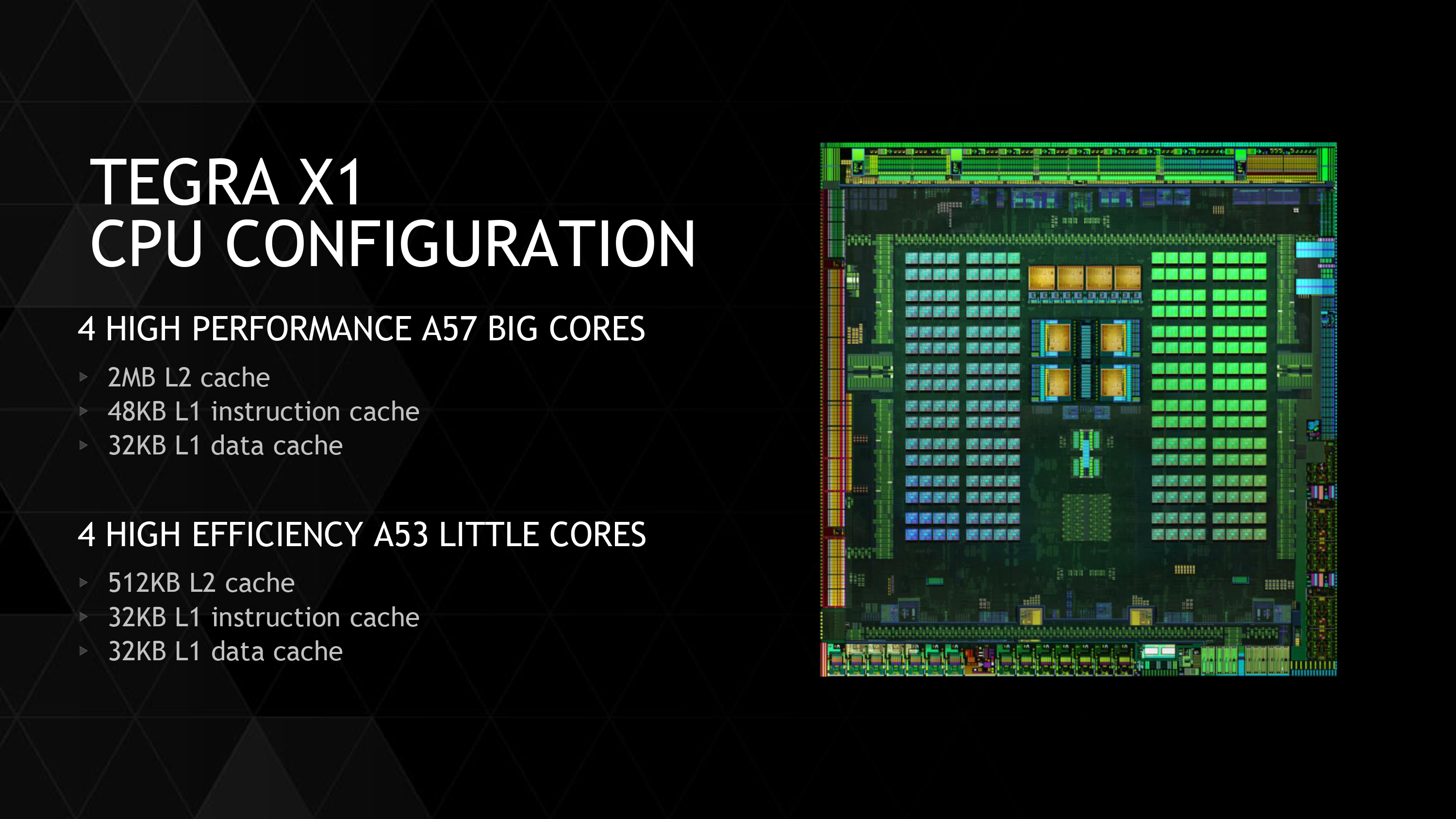
I'm expecting the same CPU and GPU config as TX1, maybe with the A53s removed (But at 0.7mm2, they may not bother removing them), and maybe a redesigned memory controller and caches, but not anything drastically different to a TX1.

")