• Hey, guest user. Hope you're enjoying NeoGAF! Have you considered registering for an account? Come join us and add your take to the daily discourse.

Next-Gen PS5 & XSX |OT| Console tEch threaD

Status
Not open for further replies.

Marlenus

Member
ROP is not related to the the number of CUs.
TMUs is.

If Xbox has 2 SEs then it probably has 64ROPa.

Rops are not linked to SEs. There can be as many or as few as the designers spec for. AMD have tended to stick to 32 per SE but we only have 2 tiers of chips in Navi 10 and Navi 14.
 

PaintTinJr

Member
Given how fast pages get added to the thread, Did anybody explain how in actual gameplay... when a controller is continuously feeding inputs to the CPU/CPU memory at double frame-rate or more, and then updating game state in CPU memory at the same rate; leading to updating the GPU/GPU memory continuously at half rate or more, how the memory bandwidth of the XsX 16GB isn’t on average 336GB/s?

Similarly, other than speculating about keeping costs down, was there a reason for the different sized modules that lead to the split memory in XsX? Has anyone speculated that it might be for thermal reasons to leave more headroom for them pushing the GPU clock higher. My thinking is, that if you were warming or cooling something in an ambient temperature you increase surface area to increase the rate of temperature change. Smaller modules means more area and faster cooling.
 

ethomaz

Banned
Rops are not linked to SEs. There can be as many or as few as the designers spec for. AMD have tended to stick to 32 per SE but we only have 2 tiers of chips in Navi 10 and Navi 14.
Nope.
You have 32ROPs per SE unless AMD drastic changes that with RDNA2 so that is why I used “probably”.

Another possibility is Xbox having more than 2SEs but that is a bit trick and BigNavi will tell is it that is possible.

BTW if that pic is true I stronge believe in 2SEs.

Xbox-Die-Feature.jpg
 
Last edited:

icerock

Member
That is how Cerny explained.
Eurogamer has an article about it too.
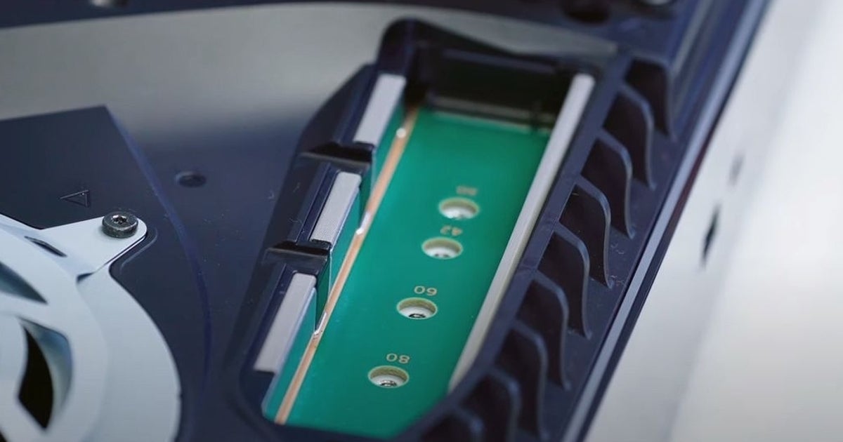
There is no SSD on motherboard... the SSD is on PCI-E 4.0 MVMe M.2 slot.


There are two PS5 expanded storage options for the PS5:

  • Replacing the internal drive within the PS5 with a Sony-certified, off-the-shelf SSD
  • Plugging in an external hard drive

I put it down to interpretation issues, with what you're suggesting is that, Sony are offering PS5 storage upgrade, and not expansion. Which is obviously not true if you scroll through the article, it clearly says 'Internal storage' and 'Expandable Storage -NVMe SSD Slot'. And next to it, reads 'Replaceable internal HDD' for PS4....

4Z9cqPD.png
 
That is how Cerny explained.
Eurogamer has an article about it too.
There is no SSD on motherboard... the SSD is on PCI-E 4.0 MVMe M.2 slot.


There are two PS5 expanded storage options for the PS5:

  • Replacing the internal drive within the PS5 with a Sony-certified, off-the-shelf SSD
  • Plugging in an external hard drive

Hmm, interesting...if that is the case when I wonder if Sony will release a 1st party upgrade drive using their custom 12 channel interface which would run just as fast if not faster than the stock drive versus getting an off the shelf NVMe?
 

ethomaz

Banned
Hmm, interesting...if that is the case when I wonder if Sony will release a 1st party upgrade drive using their custom 12 channel interface which would run just as fast if not faster than the stock drive versus getting an off the shelf NVMe?
That is why I believe will need a drive that match the Sony requirements.

But hey that is how Eurogamer though based in Cerny talk.

Maybe they did not explained right and there is two SSD slots... one internal and other expandable.
 
Last edited:
That is why I believe will need a drive that match the Sony requirements.

The only reason it makes me feel that it is soldered on though if during the presentation when he talked about the NVMe drive he says "add storage to whatever we put in the console" which leads me to believe that the initial 825GB is not removable. I am not saying your wrong, but Sony needs to clarify it a little more since it is a little confusing.


He also references that the additional NVMe storage connects through the custom I/O unit just like their SSD does.

 
Last edited:

Marlenus

Member
Nope.
You have 32ROPs per SE unless AMD drastic changes that with RDNA2 so that is why I used “probably”.

Another possibility is Xbox having more than 2SEs but that is a bit trick and BigNavi will tell is it that is possible.

AMD have only ever used 32 rops per SE but with two chips saying that is the limit or that is a requirement is premature without further information.

Even reading the white paper just tells you how they laid out Navi 10 and Navi 14 is different because it has 12 WGPs per SE rather than 10 like Navi 10 has.

If Xbox is using 2 SEs that means 14 WGPs per SE which is even more than Navi 14 so does not fit with previous layouts. More SEs would mean an asymmetric layout which we have never seen either. Given that the layout is unique no matter how the resources are split suggesting that they are sticking rigidly with 8 RBs per SE seems presumptuous.
 

ethomaz

Banned
AMD have only ever used 32 rops per SE but with two chips saying that is the limit or that is a requirement is premature without further information.

Even reading the white paper just tells you how they laid out Navi 10 and Navi 14 is different because it has 12 WGPs per SE rather than 10 like Navi 10 has.

If Xbox is using 2 SEs that means 14 WGPs per SE which is even more than Navi 14 so does not fit with previous layouts. More SEs would mean an asymmetric layout which we have never seen either. Given that the layout is unique no matter how the resources are split suggesting that they are sticking rigidly with 8 RBs per SE seems presumptuous.
That is why I if there is any change is how AMD design RDNA we will see with BigNavi that is probably the design AMD took inspiration to Xbox.

Said that RDNA has all the limitations of GCN yet it just make these limitations a bit bigger and not that big exactly.
 
Last edited:

scie

Member
The only reason it makes me feel that it is soldered on though if during the presentation when he talked about the NVMe drive he says "add storage to whatever we put in the console" which leads me to believe that the initial 825GB is not removable. I am not saying your wrong, but Sony needs to clarify it a little more since it is a little confusing.

I am thinking the same thing. Modern NVME drives have 1 -4 NAND chips on them. Sony´s solution is a 12 channel interface with 12 chips, so you can read and write to each chip simultaneously, which is a huge benefit! But if you replace this drive with existing NVMEs you will get less chips and even 7Gbit/s won´t make the difference up. So in my opinion the Sony SSD is soldered to the board and you will get an additional NVME slot.
 

Imtjnotu

Member
That is how Cerny explained.
Eurogamer has an article about it too.
There is no SSD on motherboard... the SSD is on PCI-E 4.0 MVMe M.2 slot.


There are two PS5 expanded storage options for the PS5:

  • Replacing the internal drive within the PS5 with a Sony-certified, off-the-shelf SSD
  • Plugging in an external hard drive
Your own link shows it has an internal 825gb and an expandable nvme slot. PS5's internal isn't removable
 
I am thinking the same thing. Modern NVME drives have 1 -4 NAND chips on them. Sony´s solution is a 12 channel interface with 12 chips, so you can read and write to each chip simultaneously, which is a huge benefit! But if you replace this drive with existing NVMEs you will get less chips and even 7Gbit/s won´t make the difference up. So in my opinion the Sony SSD is soldered to the board and you will get an additional NVME slot.

Without a teardown of the hardware or a direct question to Cerny, it's impossible to know but I think that is soldered as well with an additional free slot. Why Sony would allow people to REMOVE a Super SSD that doesn't even exist on the market? One of the main selling points of the machine?
 

CJY

Banned
I hope Sony have thought about this. Hypothetically, would it add a lot to the BOM having two slots?
Repair-ability probably plays a part in the cost/benefit decision of whether to include a replaceable internal NVMe slot. They'll have to figure out what the failure-rate is and whether the cost of replacing the whole board in the failed machines is worth the additional cost of having a removeable/replacable internal drive. There is more to it than just calculating the BOM.

For me, in a closed system such as a console, the less reason you give the user to open the console, the better, particular now that it's unlwaful to void a user's warranty for doing so.

Regarding the cooling system, Sony have struggled with their solution for two gens now. Much of the problems seemingly comes from the thermal compound they are using. I can see Sony forgoing the IHS this time and fusing their cooling solution directly to the chips themselves. The teardown is going to be amazing. I think I'll preorder that day.
 
I can see Sony forgoing the IHS this time and fusing their cooling solution directly to the chips themselves. The teardown is going to be amazing. I think I'll preorder that day.

I had to google direct die cooling and IHS.

Why do think Sony haven't done it before? Is that expensive?
 

Disco_

Member
Yes, even MS' own developers agree that higher frequency and narrow is preferable, MS' own words:

"And so for them to go wider, for them to go to 14 hardware threads, it means that they have the system to do it, but then, you have to have workloads that split even more effectively across them. And so we're actually finding that the vast majority of developers - talking with them about the their choices for launch - the vast majority are going to go with the SMT disabled and the higher clock."

This is on the CPU. Same applies but even more to the GPU. So Cerny has made a spot on choice again, quite visionary actually to come to that decision 'what if we could run a console GPU at 2230Mhz core clock, and what can we do to achieve that?' as the benefit is massive, and preferable to the inefficiencies that go with a 52 CU approach from MS with 400Mhz lower clocks, as all of those 52 CUs are hard to saturate, hence 'inefficiencies'.

The solution for PS5 is some exotic cooling solution that we'll find out about at the reveal and a unique variable frequency on the CPU/GPU (plus MS' Smartshift tech).
That's not what they're saying. After the launch period, pretty much everyone will use SMT. It doesn't make sense not to. You gain 30% performance with a <5% clock reduction.
When MS spoke about not using SMT, they specifically mentioned launch and cross gen games as it would be easier for devs to match the 7cores of xbone and 7 cores of xsx.

No you're completely wrong. Using your example, the 2080 Ti should be more efficient than the 2080S then right? It's got lower clocks but more transistors.

power-gaming-average.png


So which is it?

Also, again, you're being selective. If 52CUs at lower clocks is more efficient, then Series X is 'ramping up the voltage' to hit 3.8Ghz on the CPU.

To clarify - you think an APU with a 52 CU GPU @ 1800Mhz and a CPU @ 3.8Ghz is more efficient than an APU with a 36 CU GPU @ 2200Mhz and a CPU @ 3.5Ghz?
Have you actually used a 2080 or 2080 ti? Both cards pretty much run >2000mhz out of the box. Don't look at Nvidia marketing. They use lower numbers to show they have better efficiency while also being more powerful than AMD even though official specs make them look inferior.


CPU and GPU is entirely different. Scaling threads across CPUs is far more challenging than loading up all the shaders in a GPU.

If it wasn't the 2080Ti would not be faster than the 2080S.

52CUs at a more reasonable clock speed is far far far more efficient than ramping up the voltage to hit 2.23Ghz that the PS5 is doing.
This is usually true, but unless you've seen the efficiency curve for rdna2, how can you know 2200mhz isn't still in the sweet spot or close to it? Just basing all this off those desktop Navi charts? If we don't see 2200mhz desktop cards from AMD, then we can likely infer Sony made an oopsie.
 
Repair-ability probably plays a part in the cost/benefit decision of whether to include a replaceable internal NVMe slot. They'll have to figure out what the failure-rate is and whether the cost of replacing the whole board in the failed machines is worth the additional cost of having a removeable/replacable internal drive. There is more to it than just calculating the BOM.

For me, in a closed system such as a console, the less reason you give the user to open the console, the better, particular now that it's unlwaful to void a user's warranty for doing so.

A simple expansion that you can slot similar to XSEX is preferable then. Why not go that route? They can profit from it too.
 

CJY

Banned
I had to google direct die cooling and IHS.

Why do think Sony haven't done it before? Is that expensive?
It's not necassarily more expensive, but will require a totally custom cooling solution and chips normally just come with the IHS as standard. Overall whatever Sony are doing with the cooling, it's going to be more expensive than what they did in their previous consoles, that's a certainty. What I speak of with the IHS is just a very tiny part of their solution and it's possibly they won't even do that, but I think it makes a lot more sense. It's more reliable and would cool more efficiently.
 

CJY

Banned
A simple expansion that you can slot similar to XSEX is preferable then. Why not go that route? They can profit from it too.
I reckon they just don't want to go down that route of having proprietary expansion storage. It's a big positive since PS2 that you're able to use off-the-shelf expansion. I think it's the right thing and reduces retailer liability greatly in having to stock the things as well.

Sony might release their own branded drives anyway, but I have my doubts about that.
 

ethomaz

Banned
I am thinking the same thing. Modern NVME drives have 1 -4 NAND chips on them. Sony´s solution is a 12 channel interface with 12 chips, so you can read and write to each chip simultaneously, which is a huge benefit! But if you replace this drive with existing NVMEs you will get less chips and even 7Gbit/s won´t make the difference up. So in my opinion the Sony SSD is soldered to the board and you will get an additional NVME slot.
Is 7GB/s only 4 chips?
I thought you increase the speed with more modules.
 
Last edited:
I reckon they just don't want to go down that route of having proprietary expansion storage. It's a big positive since PS2 that you're able to use off-the-shelf expansion. I think it's the right thing and reduces retailer liability greatly in having to stock the things as well.

Sony might release their own branded drives anyway, but I have my doubts about that.

But if by going that route means you have to replace the 825GB one before you can expand your storage then I think the proprietary easily slottable card is the better way to go.

I mean who can afford a 2-3TB SSD at 6Gbps. Putting 1TB would not make sense.
 

CJY

Banned
But if by going that route means you have to replace the 825GB one before you can expand your storage then I think the proprietary easily slottable card is the better way to go.

I mean who can afford a 2-3TB SSD at 6Gbps. Putting 1TB would not make sense.
OK, i wasn't following the conversation properly I guess. Are you saying some people believe that if you expand the storage using an external NVMe that the internal 825 will no longer work?
 

Disco_

Member
But if by going that route means you have to replace the 825GB one before you can expand your storage then I think the proprietary easily slottable card is the better way to go.

I mean who can afford a 2-3TB SSD at 6Gbps. Putting 1TB would not make sense.
Internal drive isn't replaceable. External storage has its own slot. You're not replacing you're expanding.
Ps5 and xsx expansion works in the same exact way, one uses a modified m.2 socket while the other uses regular m. 2.
 

nosseman

Member
Have you actually used a 2080 or 2080 ti? Both cards pretty much run >2000mhz out of the box. Don't look at Nvidia marketing. They use lower numbers to show they have better efficiency while also being more powerful than AMD even though official specs make them look inferior.

The 2080 Ti is clocked quite a bit lower than 2080 Super but is still faster thanks to the "wider" render configuration.

Just look at any benchmark (where they use stock settings and reference design).

2080 Ti:
Stock clock: Boost Clock 1545 MHz
Shading Units 4352
TMUs 272
ROPs 88
SM Count 68

2080 Super:
Stock clock: Boost Clock 1815 MHz
Shading Units 3072
TMUs 192
ROPs 64
SM Count 48
 

ethomaz

Banned
I find that unrealistic.
That what you find in Eurogamer article based on Cerny talk.


How you can expand and upgrade PS5 hard drive storage
There are two PS5 expanded storage options for the PS5:

  • Replacing the internal drive within the PS5 with a Sony-certified, off-the-shelf SSD
  • Plugging in an external hard drive
Though Sony doesn't have to supply these options, there are caveats to what you can use or what you can use them for.
 
Last edited:

Bo_Hazem

Banned
DIdn't someone already say that this kraken isn't the same as RAD gametools kraken that can be found here: http://www.radgametools.com/oodlekraken.htm?

I believe there are not just one for customers, but that one is specialized in images, or maybe another company. But it's a joke anyway :lollipop_tears_of_joy:

EDIT: Compression rate is similar as well, so I guess it's not just one method. 5.5GB/s to 22GB/s is 75%.
 
Last edited:

ethomaz

Banned
I'm gonna take a look. Thanks.
There is more.


Replacing the internal SSD with a larger drive

The internal SSD can be replaced with a bigger hard drive with an off-the-shelf drive - meaning NVMe PC drives will work on your console.


They are clearly saying there is no addiction slot... it is only one PCI-E 4.0 M.2 NVMe slot where the original SSD is... you can replace it.
 
Last edited:

scie

Member
Is 7GB/s only 4 chips?
I thought you increase the speed with more modules.

Well, it depends and also the onboard controller is important. Most of the current PCIE4 1Tb NVMEs have just 2 chips and those 2 chips take almost half of the space of a NVME board. Samsungs 980 Pro has 6500 MB/s with just 2 chips.
 
Last edited:
Status
Not open for further replies.
Top Bottom